FIELD OF THE INVENTION
This invention relates generally to the field of
lubricants, and more particularly to a method for applying
lubricants to micromachines.
BACKGROUND OF THE INVENTION
Micromechanical devices include familiar structures such as
motors, wheels and gears, but are of the order of microns in
size. They also include specialized mechanical structures such
as accelerometers and spatial light modulators. Mechanical
structures, regardless of size, typically suffer from friction
and sticking between moving parts. The moving parts come into
contact with other moving parts or with non-moving parts. The
parts can be worn down by friction and sticking and the parts
can stick together, preventing the machine from operating.
Unique problems occur with micromechanical devices.
Because of their minute size, it is difficult to protect the
parts to avoid the problems of sticking and friction. The
protectant may be a lubricant or other coating on the surfaces
of the moving and non-moving parts. The coating or film must be
extremely thin so that it does not interfere with the operation
of the device. A thick film may cause the moving parts to be
blocked or jammed.
On the other hand, a film that is not robust will not
adequately protect the surfaces of the devices, resulting in
device failure. The film should preferably have high molecular
weight to be robust, low surface energy to reduce adhesion and
lower the coefficient of friction, and should bond to the
surface. Therefore, the selection of materials becomes a
challenge.
In previous attempts to protect or passivate the surfaces
of these devices, perfluordecanoic acid has been used (PFDA).
PFDA forms an oriented monolayer on the surfaces of the device.
A monolayer is a layer that is one molecule thick. This
approach is shown in US Patent 5,331,454, issued July 19, 1994.
However, only a weak chemical bond exists between the oriented
monolayer and the aluminum surface shown in the embodiments of
the above referenced patent after the monolayer has been
applied.
Another difficulty with micromechanical device protectants
is methods of application. The small size and delicacy of the
moving parts prevent use of standard techniques for applying
protectants which can destroy the device with the pressure from
the application.
The monolayer in that patent was applied by chemical vapor
deposition. In this process, a device with micromechanical
structures was placed in an oven chamber with the PFDA. When
heated the PFDA formed a vapor that deposited upon activated
surfaces of the micromechanical devices. In that approach, the
surfaces of the devices were activated by an oxygen/fluorine
plasma.
In another approach, seen in US Patent 5,403,665, issued
April 4, 1995, the surface is activated by a series of
transition baths, a complicated and very precise process.
Neither of these approaches results in an easily applied
monolayer protectant bonded to the surfaces.
SUMMARY OF THE INVENTION
One aspect of the invention is a protective coating for
micromechanical devices. The protective coating is a monolayer
of molecules that form a bond to the surface of the device and
to each adjacent molecule, resulting in a robust and effective
protective coating of high molecular weight. The monolayer is
formed by either vapor or liquid deposition.
In embodiments of both techniques, the devices are cleaned
in a UV/O3 cleaning process and the surfaces of the device are
exposed to a chlorosilane material causing a reaction that forms
the coating. In embodiments of the liquid technique the devices
are immersed in a solution of the material in a container, rinsed and removed
from the container and then baked. In embodiments of the vapor
technique the device is placed in a container with a small
amount of the material in the container. After a time interval,
the device is removed and baked.
It is an advantage of the invention in that it provides a
robust protective coating for surfaces of micromechanical
devices.
It is a further advantage of the invention in that the
protective coating both bonds to the surface and to adjacent
molecules in the coating.
BRIEF DESCRIPTION OF THE DRAWINGS
For a more complete understanding of the present invention
and for further advantages thereof, reference is now made to the
following Detailed Description taken in conjunction with the
accompanying Drawings in which:
DETAILED DESCRIPTION OF THE PREFERRED EMBODIMENTS
Figure 1 shows a chlorosilane species molecule used in one
embodiment of the invention. This molecule 10 has a head group
12 which consists of a partially chlorinated silicon atom, and
an alkyl-chain tail 14. The tail may or may not be fluorinated.
These molecules react with water or hydroxyl species on the
surface of the devices, forming a strong bond to the surface and
between the adjacent silane molecules. In micromechanical
devices having aluminum surfaces, the reaction occurs between
the SiCl3 group shown in Figure 1 and Al2O3 on the surface of the
device, plus water and/or hydroxyl species. A byproduct of this
process is HCl. The resulting bonds are shown in Figure 2.
In Figure 2, the aluminum on the surfaces 16) and 18 has
bonded with the silane molecules. Additionally, the silanes
have bonded to the adjacent silane molecules, something that did
not occur in the previous approaches to this problem. This
chemical reaction results in the surfaces 16 and 18 having a
strongly bonded, robust monolayer film with a high molecular
weight.
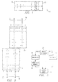
Figure 3 shows two embodiments of a method for depositing
the film. It can be deposited in either a liquid or vapor
process. Regardless of which is used, the device preparation is
the same and both involve exposing the device to the material to
form the coating.
A unique UV/O3 cleaning step 20 is used to clean and prepare
the surface for deposition. The step uses room air which is
somewhat humid, leaving the device surface covered with water
and/or hydroxyl species as well as removing any organic
contamination.
The exposure process in the liquid flow has two steps. The
devices are immersed in a 1% (v/v) solution in toluene in a dry
nitrogen filled glove bag for 30 seconds to 1 hour, at step 22.
In step 24 the devices are rinsed with fresh toluene and removed
from the glove bag. In step 26 they are placed in a vacuum oven
for baking for a time interval that varies from 20 minutes to 1
hour. Experiments have shown that 30 minutes seems optimal.
The baking step has several results. It removes any
residual solvent and reaction products, removes any excess
reactants, completes the reaction with the surface and completes
the cross-linking between adjacent silane molecules.
In the vapor technique, exposure is achieved at step 28
where the devices to be coated are placed in a container in a
water free atmosphere, such as a nitrogen purged glove bag. A
few drops of one of the above materials, for example, are then
placed in the lid of the container and the lid placed on the
container. The container remains at room temperature or is
brought to an elevated temperature to speed the process. After
a time interval the part is removed from the container and
baked. The time interval for the part to remain in the
container may vary from 20 minutes to 2 hours, with 40 minutes
seeming optimal in experiments. The baking step 26 may be for
times ranging from four to thirty minutes, with 30 minutes
appearing optimal in experiments.
The vapor deposition technique has advantages over the
liquid. No solvent like toluene is used, lessening
environmental concerns as well as eliminating the need to remove
solvent from the devices. Additionally, the lack of a solvent
means that no drying is required and collapse of the
micromechanical device due to surface tension is eliminated.
Films have been made using this technique from 1H, 1H, 2H, 2H,
perfluorodecyltrichlorosilane; 1H, 1H, 2H, 2H,
pefluorodecyldichloromethylsilane; 1H, 1H, 2H, 2H,
perfluorooctylchlorodimethylsilane, octadecyltrichlorosilane,
octyltrichlorosilane, propyltrichlorosilane, and
dodecyltrichlorosilane.
In experiments, micromechanical devices were coated using
the vapor phase technique. The devices used were
micromechanical spatial light modulator arrays comprising
individual mirror elements suspended on posts over addressing
and landing electrodes. When the individual mirrors are
addressed by the address electrodes, electrostatic forces cause
them to move and touch down on the landing electrodes. When
they receive new data, they are given a reset pulse voltage to
lift them off of the landing electrode. In devices that have
undergone this process, 90% of them worked without requiring any
kind of reset. PFDA processed devices required the reset pulse
and required higher voltages to move the mirrors. The use of
these devices is only an example of the improvements caused by
these films and is in no way intended to limit the use of these
films to these types of structures.
A Sessile Drop technique measured the surface energies of
these films. In this technique a drop of liquid is placed on a
plane surface and the angle between the side of the drop and the
plane is measured. The quality of a monolayer can be estimated
from these wetting measurements. The contact angles measured on
the films ranged from 88 to 102 degrees with diiodomethane and
up to 115 degrees with water. Additionally, these films seem to
be very robust. A series of treatments were performed with the
following results: high pressure water wash following by a 100°
C bake - changed the diiodomethane angle by only 4 degrees;
soap and water wash - no change; one hour soak in acetone - no
change; one hour soak in HOT sulphuric acid plus a strong
oxidizer followed by a fifteen minute water wash - no change;
one and a half hours in a UV/O3 oven - no change; forty second 02
+ NF3 ash in a plasma reactor - water contact angle reduced to
only 55 degrees, but film still partially present; and a
supercritical CO2 clean - diiodomethane contact angle reduced to
75 degrees (about half of film left). These results demonstrate
the robustness and passivity of these films.
This process differs from the current state of the art in
several ways. Among those are the use of the surface
preparation using UV/O3, the choice of a fluorinated precursor
in some embodiments, and in the case of the vapor technique, a
non-fluid based application.
Thus, although there has been described to this point a
particular embodiment for a material and process for
micromechanical device protection, it is not intended that such
specific references be considered as limitations upon the scope
of this invention.