EP0845301A1 - Procédé pour appliquer un lubrifiant - Google Patents
Procédé pour appliquer un lubrifiant Download PDFInfo
- Publication number
- EP0845301A1 EP0845301A1 EP97309345A EP97309345A EP0845301A1 EP 0845301 A1 EP0845301 A1 EP 0845301A1 EP 97309345 A EP97309345 A EP 97309345A EP 97309345 A EP97309345 A EP 97309345A EP 0845301 A1 EP0845301 A1 EP 0845301A1
- Authority
- EP
- European Patent Office
- Prior art keywords
- exposing
- container
- activated
- step comprises
- monolayer
- Prior art date
- Legal status (The legal status is an assumption and is not a legal conclusion. Google has not performed a legal analysis and makes no representation as to the accuracy of the status listed.)
- Withdrawn
Links
Images
Classifications
-
- B—PERFORMING OPERATIONS; TRANSPORTING
- B82—NANOTECHNOLOGY
- B82Y—SPECIFIC USES OR APPLICATIONS OF NANOSTRUCTURES; MEASUREMENT OR ANALYSIS OF NANOSTRUCTURES; MANUFACTURE OR TREATMENT OF NANOSTRUCTURES
- B82Y30/00—Nanotechnology for materials or surface science, e.g. nanocomposites
-
- C—CHEMISTRY; METALLURGY
- C23—COATING METALLIC MATERIAL; COATING MATERIAL WITH METALLIC MATERIAL; CHEMICAL SURFACE TREATMENT; DIFFUSION TREATMENT OF METALLIC MATERIAL; COATING BY VACUUM EVAPORATION, BY SPUTTERING, BY ION IMPLANTATION OR BY CHEMICAL VAPOUR DEPOSITION, IN GENERAL; INHIBITING CORROSION OF METALLIC MATERIAL OR INCRUSTATION IN GENERAL
- C23C—COATING METALLIC MATERIAL; COATING MATERIAL WITH METALLIC MATERIAL; SURFACE TREATMENT OF METALLIC MATERIAL BY DIFFUSION INTO THE SURFACE, BY CHEMICAL CONVERSION OR SUBSTITUTION; COATING BY VACUUM EVAPORATION, BY SPUTTERING, BY ION IMPLANTATION OR BY CHEMICAL VAPOUR DEPOSITION, IN GENERAL
- C23C26/00—Coating not provided for in groups C23C2/00 - C23C24/00
-
- B—PERFORMING OPERATIONS; TRANSPORTING
- B05—SPRAYING OR ATOMISING IN GENERAL; APPLYING FLUENT MATERIALS TO SURFACES, IN GENERAL
- B05D—PROCESSES FOR APPLYING FLUENT MATERIALS TO SURFACES, IN GENERAL
- B05D1/00—Processes for applying liquids or other fluent materials
- B05D1/18—Processes for applying liquids or other fluent materials performed by dipping
- B05D1/185—Processes for applying liquids or other fluent materials performed by dipping applying monomolecular layers
-
- B—PERFORMING OPERATIONS; TRANSPORTING
- B05—SPRAYING OR ATOMISING IN GENERAL; APPLYING FLUENT MATERIALS TO SURFACES, IN GENERAL
- B05D—PROCESSES FOR APPLYING FLUENT MATERIALS TO SURFACES, IN GENERAL
- B05D1/00—Processes for applying liquids or other fluent materials
- B05D1/60—Deposition of organic layers from vapour phase
-
- B—PERFORMING OPERATIONS; TRANSPORTING
- B82—NANOTECHNOLOGY
- B82Y—SPECIFIC USES OR APPLICATIONS OF NANOSTRUCTURES; MEASUREMENT OR ANALYSIS OF NANOSTRUCTURES; MANUFACTURE OR TREATMENT OF NANOSTRUCTURES
- B82Y40/00—Manufacture or treatment of nanostructures
Definitions
- This invention relates generally to the field of lubricants, and more particularly to a method for applying lubricants to micromachines.
- Micromechanical devices include familiar structures such as motors, wheels and gears, but are of the order of microns in size. They also include specialized mechanical structures such as accelerometers and spatial light modulators. Mechanical structures, regardless of size, typically suffer from friction and sticking between moving parts. The moving parts come into contact with other moving parts or with non-moving parts. The parts can be worn down by friction and sticking and the parts can stick together, preventing the machine from operating.
- the protectant may be a lubricant or other coating on the surfaces of the moving and non-moving parts.
- the coating or film must be extremely thin so that it does not interfere with the operation of the device. A thick film may cause the moving parts to be blocked or jammed.
- the film should preferably have high molecular weight to be robust, low surface energy to reduce adhesion and lower the coefficient of friction, and should bond to the surface. Therefore, the selection of materials becomes a challenge.
- PFDA perfluordecanoic acid
- micromechanical device protectants Another difficulty with micromechanical device protectants is methods of application.
- the small size and delicacy of the moving parts prevent use of standard techniques for applying protectants which can destroy the device with the pressure from the application.
- the monolayer in that patent was applied by chemical vapor deposition.
- a device with micromechanical structures was placed in an oven chamber with the PFDA.
- the PFDA formed a vapor that deposited upon activated surfaces of the micromechanical devices.
- the surfaces of the devices were activated by an oxygen/fluorine plasma.
- the protective coating is a monolayer of molecules that form a bond to the surface of the device and to each adjacent molecule, resulting in a robust and effective protective coating of high molecular weight.
- the monolayer is formed by either vapor or liquid deposition.
- the devices are cleaned in a UV/O 3 cleaning process and the surfaces of the device are exposed to a chlorosilane material causing a reaction that forms the coating.
- the devices are immersed in a solution of the material in a container, rinsed and removed from the container and then baked.
- the device is placed in a container with a small amount of the material in the container. After a time interval, the device is removed and baked.
- FIG. 1 shows a chlorosilane species molecule used in one embodiment of the invention.
- This molecule 10 has a head group 12 which consists of a partially chlorinated silicon atom, and an alkyl-chain tail 14.
- the tail may or may not be fluorinated.
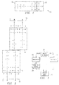
- Figure 3 shows two embodiments of a method for depositing the film. It can be deposited in either a liquid or vapor process. Regardless of which is used, the device preparation is the same and both involve exposing the device to the material to form the coating.
- a unique UV/O 3 cleaning step 20 is used to clean and prepare the surface for deposition.
- the step uses room air which is somewhat humid, leaving the device surface covered with water and/or hydroxyl species as well as removing any organic contamination.
- the exposure process in the liquid flow has two steps.
- the devices are immersed in a 1% (v/v) solution in toluene in a dry nitrogen filled glove bag for 30 seconds to 1 hour, at step 22.
- the devices are rinsed with fresh toluene and removed from the glove bag.
- step 26 they are placed in a vacuum oven for baking for a time interval that varies from 20 minutes to 1 hour. Experiments have shown that 30 minutes seems optimal.
- the baking step has several results. It removes any residual solvent and reaction products, removes any excess reactants, completes the reaction with the surface and completes the cross-linking between adjacent silane molecules.
- step 28 exposure is achieved at step 28 where the devices to be coated are placed in a container in a water free atmosphere, such as a nitrogen purged glove bag. A few drops of one of the above materials, for example, are then placed in the lid of the container and the lid placed on the container. The container remains at room temperature or is brought to an elevated temperature to speed the process. After a time interval the part is removed from the container and baked. The time interval for the part to remain in the container may vary from 20 minutes to 2 hours, with 40 minutes seeming optimal in experiments. The baking step 26 may be for times ranging from four to thirty minutes, with 30 minutes appearing optimal in experiments.
- the vapor deposition technique has advantages over the liquid. No solvent like toluene is used, lessening environmental concerns as well as eliminating the need to remove solvent from the devices. Additionally, the lack of a solvent means that no drying is required and collapse of the micromechanical device due to surface tension is eliminated.
- Films have been made using this technique from 1H, 1H, 2H, 2H, perfluorodecyltrichlorosilane; 1H, 1H, 2H, 2H, pefluorodecyldichloromethylsilane; 1H, 1H, 2H, 2H, perfluorooctylchlorodimethylsilane, octadecyltrichlorosilane, octyltrichlorosilane, propyltrichlorosilane, and dodecyltrichlorosilane.
- micromechanical devices were coated using the vapor phase technique.
- the devices used were micromechanical spatial light modulator arrays comprising individual mirror elements suspended on posts over addressing and landing electrodes. When the individual mirrors are addressed by the address electrodes, electrostatic forces cause them to move and touch down on the landing electrodes. When they receive new data, they are given a reset pulse voltage to lift them off of the landing electrode. In devices that have undergone this process, 90% of them worked without requiring any kind of reset. PFDA processed devices required the reset pulse and required higher voltages to move the mirrors. The use of these devices is only an example of the improvements caused by these films and is in no way intended to limit the use of these films to these types of structures.
- a Sessile Drop technique measured the surface energies of these films.
- a drop of liquid is placed on a plane surface and the angle between the side of the drop and the plane is measured.
- the quality of a monolayer can be estimated from these wetting measurements.
- the contact angles measured on the films ranged from 88 to 102 degrees with diiodomethane and up to 115 degrees with water. Additionally, these films seem to be very robust.
- This process differs from the current state of the art in several ways. Among those are the use of the surface preparation using UV/O 3 , the choice of a fluorinated precursor in some embodiments, and in the case of the vapor technique, a non-fluid based application.
Applications Claiming Priority (2)
| Application Number | Priority Date | Filing Date | Title |
|---|---|---|---|
| US3165796P | 1996-11-20 | 1996-11-20 | |
| US31657P | 1996-11-20 |
Publications (1)
| Publication Number | Publication Date |
|---|---|
| EP0845301A1 true EP0845301A1 (fr) | 1998-06-03 |
Family
ID=21860715
Family Applications (1)
| Application Number | Title | Priority Date | Filing Date |
|---|---|---|---|
| EP97309345A Withdrawn EP0845301A1 (fr) | 1996-11-20 | 1997-11-20 | Procédé pour appliquer un lubrifiant |
Country Status (3)
| Country | Link |
|---|---|
| EP (1) | EP0845301A1 (fr) |
| JP (1) | JPH10158670A (fr) |
| KR (1) | KR19980042570A (fr) |
Cited By (4)
| Publication number | Priority date | Publication date | Assignee | Title |
|---|---|---|---|---|
| WO2001023101A2 (fr) * | 1999-09-27 | 2001-04-05 | Nanogate Gmbh | Procedes et matieres |
| US6300294B1 (en) | 1998-11-16 | 2001-10-09 | Texas Instruments Incorporated | Lubricant delivery for micromechanical devices |
| WO2004033364A2 (fr) * | 2002-10-11 | 2004-04-22 | Regents Of The University Of Minnesota | Procedes de formation de revetements sur des dispositifs micro-electromecaniques |
| US7229694B2 (en) | 2002-05-25 | 2007-06-12 | Robert Bosch Gmbh | Micromechanical component and method for producing an anti-adhesive layer on a micromechanical component |
Families Citing this family (1)
| Publication number | Priority date | Publication date | Assignee | Title |
|---|---|---|---|---|
| DE102004037902A1 (de) * | 2004-08-05 | 2006-03-16 | Robert Bosch Gmbh | Verfahren zur Abscheidung einer Anti-Haftungsschicht |
Citations (7)
| Publication number | Priority date | Publication date | Assignee | Title |
|---|---|---|---|---|
| EP0498335A1 (fr) * | 1991-02-06 | 1992-08-12 | Matsushita Electric Industrial Co., Ltd. | Méthode pour fabriquer un film adsorbé chimiquement |
| EP0501298A2 (fr) * | 1991-02-27 | 1992-09-02 | Matsushita Electric Industrial Co., Ltd. | Dispositif autolubrifiant |
| EP0571896A2 (fr) * | 1992-05-27 | 1993-12-01 | Matsushita Electric Industrial Co., Ltd. | Procédé de fabrication d'un film absorbé chimiquement |
| FR2694369A1 (fr) * | 1992-07-29 | 1994-02-04 | Lyon Ecole Centrale | Procédé de lubrification d'une pièce mécanique de frottement. |
| EP0582131A1 (fr) * | 1992-07-29 | 1994-02-09 | Matsushita Electric Industrial Co., Ltd. | Film lubrifiant et méthode pour sa préparation |
| EP0582181A1 (fr) * | 1992-07-29 | 1994-02-09 | Matsushita Electric Industrial Co., Ltd. | Film lubrifiant et méthode pour sa préparation |
| WO1995000258A1 (fr) * | 1993-06-18 | 1995-01-05 | The Regents Of The University Of California | Procede d'application de lubrifiant en monocouche sur des instruments de micro-usinage |
-
1997
- 1997-11-19 KR KR1019970060986A patent/KR19980042570A/ko not_active Application Discontinuation
- 1997-11-19 JP JP9318618A patent/JPH10158670A/ja active Pending
- 1997-11-20 EP EP97309345A patent/EP0845301A1/fr not_active Withdrawn
Patent Citations (7)
| Publication number | Priority date | Publication date | Assignee | Title |
|---|---|---|---|---|
| EP0498335A1 (fr) * | 1991-02-06 | 1992-08-12 | Matsushita Electric Industrial Co., Ltd. | Méthode pour fabriquer un film adsorbé chimiquement |
| EP0501298A2 (fr) * | 1991-02-27 | 1992-09-02 | Matsushita Electric Industrial Co., Ltd. | Dispositif autolubrifiant |
| EP0571896A2 (fr) * | 1992-05-27 | 1993-12-01 | Matsushita Electric Industrial Co., Ltd. | Procédé de fabrication d'un film absorbé chimiquement |
| FR2694369A1 (fr) * | 1992-07-29 | 1994-02-04 | Lyon Ecole Centrale | Procédé de lubrification d'une pièce mécanique de frottement. |
| EP0582131A1 (fr) * | 1992-07-29 | 1994-02-09 | Matsushita Electric Industrial Co., Ltd. | Film lubrifiant et méthode pour sa préparation |
| EP0582181A1 (fr) * | 1992-07-29 | 1994-02-09 | Matsushita Electric Industrial Co., Ltd. | Film lubrifiant et méthode pour sa préparation |
| WO1995000258A1 (fr) * | 1993-06-18 | 1995-01-05 | The Regents Of The University Of California | Procede d'application de lubrifiant en monocouche sur des instruments de micro-usinage |
Non-Patent Citations (1)
| Title |
|---|
| SUZUKI M ET AL: "CHARACTERIZATION OF MONOLAYER AND BILAYER (POLYMER/MONOLAYER) STRUCTURES FOR THEIR USE AS A LUBRICANT", THIN SOLID FILMS, vol. 160, no. 1, + INDEX, June 1988 (1988-06-01), pages 453 - 462, XP000048218 * |
Cited By (7)
| Publication number | Priority date | Publication date | Assignee | Title |
|---|---|---|---|---|
| US6300294B1 (en) | 1998-11-16 | 2001-10-09 | Texas Instruments Incorporated | Lubricant delivery for micromechanical devices |
| WO2001023101A2 (fr) * | 1999-09-27 | 2001-04-05 | Nanogate Gmbh | Procedes et matieres |
| WO2001023101A3 (fr) * | 1999-09-27 | 2001-10-25 | Nanogate Gmbh | Procedes et matieres |
| US7229694B2 (en) | 2002-05-25 | 2007-06-12 | Robert Bosch Gmbh | Micromechanical component and method for producing an anti-adhesive layer on a micromechanical component |
| DE10223359B4 (de) * | 2002-05-25 | 2011-08-11 | Robert Bosch GmbH, 70469 | Mikromechanisches Bauteil und Verfahren zur Herstellung einer Anti-Haftschicht auf einem mikromechanischen Bauteil |
| WO2004033364A2 (fr) * | 2002-10-11 | 2004-04-22 | Regents Of The University Of Minnesota | Procedes de formation de revetements sur des dispositifs micro-electromecaniques |
| WO2004033364A3 (fr) * | 2002-10-11 | 2004-10-28 | Univ Minnesota | Procedes de formation de revetements sur des dispositifs micro-electromecaniques |
Also Published As
| Publication number | Publication date |
|---|---|
| KR19980042570A (ko) | 1998-08-17 |
| JPH10158670A (ja) | 1998-06-16 |
Similar Documents
| Publication | Publication Date | Title |
|---|---|---|
| US5411769A (en) | Method of producing micromechanical devices | |
| JP4928940B2 (ja) | 酸化層により接着される多層コーティングの制御された気相堆積 | |
| US8067258B2 (en) | Protective thin films for use during fabrication of semiconductors, MEMS, and microstructures | |
| US5602671A (en) | Low surface energy passivation layer for micromechanical devices | |
| Ashurst et al. | Vapor phase anti-stiction coatings for MEMS | |
| US5476717A (en) | Material having antireflection, hydrophobic and abrasion resistance properties and process for depositing an antireflection, hydrophobic and abrasion resistant coating on a substrate | |
| WO2002090245A2 (fr) | Procedes de fabrication de dispositifs a microstructure | |
| JP3743519B2 (ja) | シリコン−酸化物薄層の製造方法 | |
| Ashurst et al. | Wafer level anti-stiction coatings for MEMS | |
| EP0746013A3 (fr) | Méthode de nettoyage et traitement d'un dispositif micromécanique | |
| US20060234413A1 (en) | Method for forming anti-stiction bumps on a micro-electro mechanical structure | |
| US7309902B2 (en) | Microelectronic device with anti-stiction coating | |
| EP1416064B1 (fr) | Méthode de revêtement de dispositifs micro-électromécaniques | |
| US20050118742A1 (en) | Method for reducing the adhesive properties of MEMS and anti-adhesion-coated device | |
| EP0845301A1 (fr) | Procédé pour appliquer un lubrifiant | |
| Almanza-Workman et al. | Water dispersible silanes for wettability modification of polysilicon | |
| US11124659B2 (en) | Method to selectively pattern a surface for plasma resistant coat applications | |
| JPH04255343A (ja) | 撥水撥油コーティング膜及びその製造方法 | |
| EP0615147B1 (fr) | Dispositifs micromécanique à miroirs déformables (-DMD-) | |
| JP5359529B2 (ja) | 撥水性物品の製造方法及び撥水性物品 | |
| US20070052132A1 (en) | Method and system for cleaning molded items | |
| US7201937B2 (en) | Methods for forming composite coatings on MEMS devices | |
| JPH05116324A (ja) | インクジエツト吐出用ノズル板およびその製造方法 | |
| DE10355038B4 (de) | Verfahren zur Beschichtung einer Oberfläche | |
| JPH10146920A (ja) | 撥水撥油性被膜を有する物品及びその形成方法 |
Legal Events
| Date | Code | Title | Description |
|---|---|---|---|
| PUAI | Public reference made under article 153(3) epc to a published international application that has entered the european phase |
Free format text: ORIGINAL CODE: 0009012 |
|
| AK | Designated contracting states |
Kind code of ref document: A1 Designated state(s): DE FR GB IT NL |
|
| AX | Request for extension of the european patent |
Free format text: AL;LT;LV;MK;RO;SI |
|
| 17P | Request for examination filed |
Effective date: 19981125 |
|
| AKX | Designation fees paid |
Free format text: DE FR GB IT NL |
|
| RBV | Designated contracting states (corrected) |
Designated state(s): DE FR GB IT NL |
|
| 17Q | First examination report despatched |
Effective date: 20021001 |
|
| GRAP | Despatch of communication of intention to grant a patent |
Free format text: ORIGINAL CODE: EPIDOSNIGR1 |
|
| GRAS | Grant fee paid |
Free format text: ORIGINAL CODE: EPIDOSNIGR3 |
|
| STAA | Information on the status of an ep patent application or granted ep patent |
Free format text: STATUS: THE APPLICATION IS DEEMED TO BE WITHDRAWN |
|
| 18D | Application deemed to be withdrawn |
Effective date: 20041224 |