EP0933377A2 - Anti-smudge agent, method of forming an anti-smudge layer, anti-reflection optical member and display device - Google Patents
Anti-smudge agent, method of forming an anti-smudge layer, anti-reflection optical member and display device Download PDFInfo
- Publication number
- EP0933377A2 EP0933377A2 EP99101960A EP99101960A EP0933377A2 EP 0933377 A2 EP0933377 A2 EP 0933377A2 EP 99101960 A EP99101960 A EP 99101960A EP 99101960 A EP99101960 A EP 99101960A EP 0933377 A2 EP0933377 A2 EP 0933377A2
- Authority
- EP
- European Patent Office
- Prior art keywords
- smudge
- agent
- layer
- display
- substrate
- Prior art date
- Legal status (The legal status is an assumption and is not a legal conclusion. Google has not performed a legal analysis and makes no representation as to the accuracy of the status listed.)
- Granted
Links
Images
Classifications
-
- G—PHYSICS
- G02—OPTICS
- G02B—OPTICAL ELEMENTS, SYSTEMS OR APPARATUS
- G02B1/00—Optical elements characterised by the material of which they are made; Optical coatings for optical elements
- G02B1/10—Optical coatings produced by application to, or surface treatment of, optical elements
- G02B1/18—Coatings for keeping optical surfaces clean, e.g. hydrophobic or photo-catalytic films
-
- C—CHEMISTRY; METALLURGY
- C09—DYES; PAINTS; POLISHES; NATURAL RESINS; ADHESIVES; COMPOSITIONS NOT OTHERWISE PROVIDED FOR; APPLICATIONS OF MATERIALS NOT OTHERWISE PROVIDED FOR
- C09D—COATING COMPOSITIONS, e.g. PAINTS, VARNISHES OR LACQUERS; FILLING PASTES; CHEMICAL PAINT OR INK REMOVERS; INKS; CORRECTING FLUIDS; WOODSTAINS; PASTES OR SOLIDS FOR COLOURING OR PRINTING; USE OF MATERIALS THEREFOR
- C09D4/00—Coating compositions, e.g. paints, varnishes or lacquers, based on organic non-macromolecular compounds having at least one polymerisable carbon-to-carbon unsaturated bond ; Coating compositions, based on monomers of macromolecular compounds of groups C09D183/00 - C09D183/16
-
- C—CHEMISTRY; METALLURGY
- C07—ORGANIC CHEMISTRY
- C07F—ACYCLIC, CARBOCYCLIC OR HETEROCYCLIC COMPOUNDS CONTAINING ELEMENTS OTHER THAN CARBON, HYDROGEN, HALOGEN, OXYGEN, NITROGEN, SULFUR, SELENIUM OR TELLURIUM
- C07F7/00—Compounds containing elements of Groups 4 or 14 of the Periodic System
- C07F7/02—Silicon compounds
- C07F7/08—Compounds having one or more C—Si linkages
- C07F7/18—Compounds having one or more C—Si linkages as well as one or more C—O—Si linkages
- C07F7/1804—Compounds having Si-O-C linkages
-
- C—CHEMISTRY; METALLURGY
- C08—ORGANIC MACROMOLECULAR COMPOUNDS; THEIR PREPARATION OR CHEMICAL WORKING-UP; COMPOSITIONS BASED THEREON
- C08G—MACROMOLECULAR COMPOUNDS OBTAINED OTHERWISE THAN BY REACTIONS ONLY INVOLVING UNSATURATED CARBON-TO-CARBON BONDS
- C08G77/00—Macromolecular compounds obtained by reactions forming a linkage containing silicon with or without sulfur, nitrogen, oxygen or carbon in the main chain of the macromolecule
- C08G77/04—Polysiloxanes
- C08G77/22—Polysiloxanes containing silicon bound to organic groups containing atoms other than carbon, hydrogen and oxygen
- C08G77/24—Polysiloxanes containing silicon bound to organic groups containing atoms other than carbon, hydrogen and oxygen halogen-containing groups
-
- G—PHYSICS
- G02—OPTICS
- G02B—OPTICAL ELEMENTS, SYSTEMS OR APPARATUS
- G02B1/00—Optical elements characterised by the material of which they are made; Optical coatings for optical elements
- G02B1/10—Optical coatings produced by application to, or surface treatment of, optical elements
-
- G—PHYSICS
- G02—OPTICS
- G02B—OPTICAL ELEMENTS, SYSTEMS OR APPARATUS
- G02B1/00—Optical elements characterised by the material of which they are made; Optical coatings for optical elements
- G02B1/10—Optical coatings produced by application to, or surface treatment of, optical elements
- G02B1/11—Anti-reflection coatings
-
- H—ELECTRICITY
- H01—ELECTRIC ELEMENTS
- H01J—ELECTRIC DISCHARGE TUBES OR DISCHARGE LAMPS
- H01J29/00—Details of cathode-ray tubes or of electron-beam tubes of the types covered by group H01J31/00
- H01J29/86—Vessels; Containers; Vacuum locks
- H01J29/89—Optical or photographic arrangements structurally combined or co-operating with the vessel
- H01J29/896—Anti-reflection means, e.g. eliminating glare due to ambient light
Definitions
- This invention relates to an anti-smudge agent for forming an anti-smudge layer on the surface of various kinds of substrate to be treated (hereinafter referred to simply as a treating substrate) and requiring an anti-smudge property, and to a method of forming an anti-smudge layer by making use of this anti-smudge agent.
- this invention relates to an anti-reflection optical member which is adapted to be applied to the surface of display screen of an optical member (such as an anti-reflection film, an optical filter, an optical lens, spectacle lens, beam splitter, prism, mirror, etc.) and a device (such as a liquid crystal display, a CRT display, a projection television, a plasma display, an EL display, etc.), to an optical functional member, and to a display device wherein this optical functional member is adhered to the surface of display screen of the display device.
- an optical member such as an anti-reflection film, an optical filter, an optical lens, spectacle lens, beam splitter, prism, mirror, etc.
- a device such as a liquid crystal display, a CRT display, a projection television, a plasma display, an EL display, etc.
- Optical members such as an anti-reflection film, an optical filter, an optical lens, spectacle lens, beam splitter, prism, mirror, etc. are liable to be soiled with smudges originating from fingerprints, skin fat, sweat, cosmetics, etc. as these members are employed by an operator. Once these members are soiled with these smudges, it is very difficult to remove them. Particularly in the case of an optical member provided with an antireflection coating, the smudge adhered to the antireflection coating stands out from the coating, thus raising a problem.
- the incident light like this external light is mirror-reflected by the surface of the display screen, thus causing a mixing of images between the reflected image and the displayed image, resulting in the deterioration of the display quality and hence the blurring of the display image.
- a reflection preventive optical member is attached to the surface of the display screen, this reflection preventive optical member being capable of preventing the reflection of light over a wide range of visible light.
- a reflection preventive optical member is a laminate film comprising a transparent substrate on the surface which a high refractive index layer and a low refractive index layer both consisting of a metal oxide are laminated.
- a reflection preventive optical member which is formed of a laminate film comprising a transparent substrate on the surface which a low refractive index layer consisting of an inorganic or organic fluorine compound is laminated.
- the aforementioned reflection preventive optical members tend to be soiled with smudges originating from fingerprints, skin fat, sweat, cosmetics, etc. as the display device provided with this reflection preventive optical member is employed by an operator.
- the surface energy of the reflection preventive film is generally as large as 60 J/m 2 or so, the reflection preventive film is more likely to be soiled with these smudges.
- the surface of the reflection preventive film is constituted by a finely roughened surface, once these smudges are adhered onto the reflection preventive film, it is very difficult to remove them. Further, there is also a problem that when these smudges are adhered to a portion of the reflection preventive film, the soiled portion becomes more reflective, thereby rendering the soiled portion to stand out from the remaining portion.
- Japanese Patent Unexamined Publication S64-86101 teaches a reflection preventive article having anti-smudge and abrasion resistive properties wherein the surface of the substrate is covered with a reflection preventive film consisting mainly of silicon dioxide, and the resultant surface is further treated with a compound containing an organosilicic substituent group.
- Japanese Patent Unexamined Publication H4-338901 teaches a CRT filter having anti-smudge and abrasion resistive properties, whose substrate surface is covered with a terminal silanol organopolysiloxane.
- Japanese Patent Publication H6-29332 teaches an anti-smudge/low reflectance plastic covered on its surface with a refection preventive film containing mono- and di-silane compounds containing polyfluoroalkyl group, and a silanized halogen, alkyl or alkoxy compound.
- Japanese Patent Unexamined Publication H7-16940 teaches an optical member comprising an optical thin film consisting mainly of silicon dioxide, on which a copolymer consisting of perfluoroalkyl(meta)acrylate and a monomer having alkoxy silane group is formed.
- the anti-smudge layer manufactured according to these conventional methods is insufficient in anti-smudge property, incapable of allowing a smudge such as fingerprints, skin fat, sweat, cosmetics, etc. to be easily removed therefrom, and poor in durability losing sharply its anti-smudge property with a repetition of use. Therefore, it is now desired to develop an anti-smudge layer which is excellent in anti-smudge property and in the durability of anti-smudge property.
- an object of this invention is to provide an anti-smudge agent, which makes it possible to obtain an anti-smudge layer which is excellent in durability of the property, capable of preventing smudges formed of fingerprints, skin fat, sweat, cosmetics, etc. from being adhered onto the surface of an optical member such as a reflection preventive film, and capable of allowing these smudges to be easily removed even if these smudges are adhered onto the optical member.
- Another object of this invention is to provide a method of forming an anti-smudge layer which is capable of easily forming an anti-smudge layer which is excellent in anti-smudge property and in the durability of the anti-smudge property.
- Still another object of this invention is to provide a optical member which is provided with the aforementioned anti-smudge layer.
- Still another object of this invention is to provide a reflection preventive optical member which is provided with the aforementioned anti-smudge layer.
- a further object of this invention is to provide an optical functional member which is provided with the aforementioned reflection preventive optical member.
- a still further object of this invention is to provide a display device whose display screen surface is constituted by the aforementioned optical functional member.
- R f2 is a linear or branched perfluoroalkyl group having 1 to 16 carbon atoms
- R 2 is a hydrolytic group
- Z is -OOCNH
- an optical member provided with an anti-smudge layer containing the aforementioned anti-smudge agent.
- a reflection preventive optical member provided with an anti-smudge layer containing the aforementioned anti-smudge agent.
- an optical functional member constituted by the aforementioned reflection preventive optical member.
- a display device provided with the aforementioned optical functional member.
- the anti-smudge agent according to this invention is characterized in that it contains a specific kind of organosilicon compound.
- the treating substrate is any kind of optical members such as an anti-reflection film, an optical filter, an optical lens, spectacle lens, beam splitter, prism, mirror, etc., to prevent smudges formed any of fingerprints, skin fat, sweat, cosmetics, etc. from being adhered onto the surface of these optical members, and furthermore, to easily remove these smudges adhered onto these optical members without deteriorating the optical properties of these optical members.
- the anti-smudge layer formed by making use of this anti-smudge agent is excellent in durability of the property.
- the anti-smudge agent according to this invention contains an organosilicon compound represented by the following general formula (1): R f2 -(OC 3 F 6 ) n2 -O-(CF 2 ) m2 -(CH 2 ) 12 -Z-(CH 2 ) s2 -Si-(R 2 ) 3 wherein R f2 is a linear or branched perfluoroalkyl group having 1 to 16 carbon atoms; R 2 is a hydrolytic group; Z is -OOCNH- or -O-; n2 is an integer of 1 to 50; m2 is an integer of 0 to 3; 12 is an integer of 0 to 3; and s2 is an integer of 1 to 6, with a proviso that these m2 and 12 meet the condition of 6 ⁇ m2+12>0.
- R f2 is a linear or branched perfluoroalkyl group having 1 to 16 carbon atoms
- R 2 is a hydrolytic group
- Z is
- the number of carbon atom of the linear or branched perfluoroalkyl group to be introduced into R f2 is preferably in the range of from 1 to 16, more preferably in the range of from 1 to 3. Therefore, most preferable examples of R f2 are -CF 3 , -C 2 F 5 , -C 3 F 7 , etc.
- hydrolytic group is -OCH 3 , -OC 2 H 5 , -OOCCH 3 , and -NH 2 .
- hydrolytic groups may be included singly or in combination of two or more kinds in the organosilicon compound constituting the anti-smudge agent of this invention.
- the n2 in the aforementioned general formula (1) should preferably be in the range of 1 to 30, more preferably in the range of 5 to 20.
- the m2 in the aforementioned general formula (1) should preferably be in the range of 1 to 2.
- the 12 in the aforementioned general formula (1) should preferably be in the range of 1 to 2.
- the s2 in the aforementioned general formula (1) should preferably be in the range of 1 to 3.
- an organosilicon compound represented by the following general formula (2D) can be obtained by allowing a fluorine resin having hydroxyl group and represented by the following general formula (2A) to react with catalyst and a isocyanate-based silane coupling agent represented by the following general formula (2C) in a solvent.
- This reaction can be advantageously proceeded by using 0.001 to 0.01 mol of C 32 H 64 O 4 Sn as a catalyst and 1 to an excess of a isocyanate-based silane coupling agent per 1 mol of a fluorine resin containing hydroxyl group and by performing the reaction at a temperature ranging from room temperature to the reflux temperature of the solvent for 2 to 72 hours.
- the solvent useful in this case it is possible to employ an ordinary perfluoroaliphatic hydrocarbon having 5 to 12 carbon atoms, such as perfluorohexane, perfluoromethylcyclohexane, perfluoro-1,3-dimethylcyclohexane, etc.; an aromatic hydrocarbon polyfluoride such as bis(trifluoromethyl) benzene; or an aliphatic hydrocarbon polyfluoride.
- an ordinary perfluoroaliphatic hydrocarbon having 5 to 12 carbon atoms such as perfluorohexane, perfluoromethylcyclohexane, perfluoro-1,3-dimethylcyclohexane, etc.
- an aromatic hydrocarbon polyfluoride such as bis(trifluoromethyl) benzene
- an aliphatic hydrocarbon polyfluoride such as bis(trifluoromethyl) benzene
- the anti-smudge agent according to this invention may include, if desired, various kinds of additives in addition to the aforementioned organometallic compounds represented by the general formula (1).
- the anti-smudge agent may contain a catalyst for promoting the hydrolysis or polycondensation of the organosilicon compounds represented by the general formula (1) or for promoting the formation of condensed urethane linkage.
- the catalyst that can be employed in the anti-smudge agent of this invention it is possible to employ hydrochloric acid, nitric acid, sulfuric acid, acetic acid, hydrofluoric acid, formic acid, phosphoric acid, oxalic acid, ammonia, aluminum acetylacetonate, dibutyltin dilaurate, octylate tin compound, sodium, sodium hydride, methane sulfonate, trifluoromethane sulfonate, paratoluene sulfonate, trifluoroacetate, etc.
- These compounds can be employed singly or in combination of two or more kinds.
- an organosilicon compound represented by the following general formula (2E) can be obtained by allowing a fluorine resin having hydroxyl group and represented by the following general formula (2A) to react with catalyst and a halogen-based silane coupling agent represented by the following general formula (2B) in a solvent.
- This reaction can be advantageously proceeded by using 1 to 1.1 excess of NaH as a catalyst and 1 to an excess of a halogen-based silane coupling agent per 1 mol of a fluorine resin containing hydroxyl group and by performing the reaction at a temperature ranging from room temperature to the reflux temperature of the solvent for 2 to 72 hours.
- the solvent useful in this case it is possible to employ an ordinary perfluoroaliphatic hydrocarbon having 5 to 12 carbon atoms, such as perfluorohexane, perfluoromethylcyclohexane, perfluoro-1,3-dimethylcyclohexane, etc.; an aromatic hydrocarbon polyfluoride such as bis(trifluoromethyl) benzene; or an aliphatic hydrocarbon polyfluoride.
- an ordinary perfluoroaliphatic hydrocarbon having 5 to 12 carbon atoms such as perfluorohexane, perfluoromethylcyclohexane, perfluoro-1,3-dimethylcyclohexane, etc.
- an aromatic hydrocarbon polyfluoride such as bis(trifluoromethyl) benzene
- an aliphatic hydrocarbon polyfluoride such as bis(trifluoromethyl) benzene
- the anti-smudge agent according to this invention may include, if desired, various kinds of additives in addition to the aforementioned organometallic compounds represented by the general formula (1).
- the anti-smudge agent may contain a catalyst for promoting the hydrolysis or polycondensation of the organosilicon compounds represented by the general formula (1) or for promoting the formation of condensed ether linkage.
- the catalyst that can be employed in the anti-smudge agent of this invention it is possible to employ hydrochloric acid, nitric acid, sulfuric acid, acetic acid, hydrofluoric acid, formic acid, phosphoric acid, oxalic acid, ammonia, aluminum acetylacetonate, dibutyltin dilaurate, octylate tin compound, sodium, sodium hydride, methane sulfonate, trifluoromethane sulfonate, paratoluene sulfonate, trifluoroacetate, etc.
- These compounds can be employed singly or in combination of two or more kinds.
- the number of carbon atom of the linear or branched perfluoroalkyl group to be introduced into R f2 is preferably in the range of from 1 to 16, more preferably in the range of from 1 to 3. Therefore, most preferable examples of R f2 are -CF 3 , -C 2 F 5 , -C 3 F 7 , etc.
- the number of carbon atom of the alkyl group to be introduced into R 3 is preferably in the range of from 1 to 10, more preferably in the range of from 1 to 3. Therefore, most preferable examples of R 3 are -CH 3 , -C 2 H 5 , -C 3 H 7 , etc.
- the compounds represented the general formula (3) may be prepared according to the following reaction formula:
- an organosilicon compound represented by the following general formula (3) can be obtained by allowing a fluorine resin having hydroxyl group and represented by the following general formula (3A) to react with catalyst and a halogen-based silane coupling agent represented by the following general formula (3B) in a solvent.
- R f2 is a linear or branched perfluoroalkyl group having 1 to 16 carbon atoms
- R 3 is an alkyl group having 1 to 10 carbon atoms
- X is a halogen atom
- n2 is an integer of 1 to 50
- m2 is an integer of 0 to 3
- 12 is an integer of 0 to 3
- s2 is an integer of 1 to 6
- a is an integer of 0 to 3
- b is an integer of 0 to 3
- c is 0 or 1
- This reaction can be advantageously proceeded by using 1 to 1.1 excess of NaH as a catalyst and 1 to an excess of a halogen-based silane coupling agent per 1 mol of a fluorine resin containing hydroxyl group and by performing the reaction at a temperature ranging from room temperature to the reflux temperature of the solvent for 2 to 72 hours.
- the solvent useful in this case it is possible to employ an ordinary perfluoroaliphatic hydrocarbon having 5 to 12 carbon atoms, such as perfluorohexane, perfluoromethylcyclohexane, perfluoro-1,3-dimethylcyclohexane, etc.; an aromatic hydrocarbon polyfluoride such as bis(trifluoromethyl) benzene; or an aliphatic hydrocarbon polyfluoride.
- an ordinary perfluoroaliphatic hydrocarbon having 5 to 12 carbon atoms such as perfluorohexane, perfluoromethylcyclohexane, perfluoro-1,3-dimethylcyclohexane, etc.
- an aromatic hydrocarbon polyfluoride such as bis(trifluoromethyl) benzene
- an aliphatic hydrocarbon polyfluoride such as bis(trifluoromethyl) benzene
- organosilicon compounds represented by the aforementioned general formula (3) can be employed singly or in combination of two or more kinds for constituting the anti-smudge agent of this invention.
- the components "a”, "b", “c” and “d” in the aforementioned general formula (3) should be differentiated.
- the anti-smudge agent according to this invention may include, if desired, various kinds of additives in addition to the aforementioned organometallic compounds represented by the general formula (3).
- the anti-smudge agent may contain a catalyst for promoting the hydrolysis or polycondensation of the organosilicon compounds represented by the general formula (3) or for promoting the formation of condensed ether linkage.
- the catalyst that can be employed in the anti-smudge agent of this invention it is possible to employ hydrochloric acid, nitric acid, sulfuric acid, acetic acid, hydrofluoric acid, formic acid, phosphoric acid, oxalic acid, ammonia, aluminum acetylacetonate, dibutyltin dilaurate, octylate tin compound, sodium, sodium hydride, methane sulfonate, trifluoromethane sulfonate, paratoluene sulfonate, trifluoroacetate, etc.
- These compounds can be employed singly or in combination of two or more kinds.
- an inorganic substrate such as a glass board, a glass board comprising an inorganic compound layer
- an organic substrate such as a transparent plastic substrate, a transparent plastic substrate comprising an inorganic compound layer
- a glass board may be mainly employed as an inorganic substrate.
- the inorganic compound to be employed for constituting the glass board comprising an inorganic compound layer it is possible to employ a metal oxide such as silicon oxide (silicon dioxide, silicon monooxide, etc.), aluminum oxide, magnesium oxide, titanium oxide, tin oxide, zirconium oxide, sodium oxide, antimony oxide, indium oxide, bismuth oxide, yttrium oxide, cerium oxide, zinc oxide, ITO (indium tin oxide), etc.; or a metal halide such as magnesium fluoride, calcium fluoride, sodium fluoride, lanthanum fluoride, cerium fluoride, lithium fluoride, thorium fluoride, etc.
- a metal oxide such as silicon oxide (silicon dioxide, silicon monooxide, etc.), aluminum oxide, magnesium oxide, titanium oxide, tin oxide, zirconium oxide, sodium oxide, antimony oxide, indium oxide, bismuth oxide, yttrium oxide, cerium oxide, zinc oxide
- the inorganic substrate or inorganic compound layer formed of any of these inorganic compounds may be of a single layer or a multi-layer.
- the inorganic compound layer functions as a reflection preventive layer and can be formed by making use of any conventional method such as a wet coating method, a PVD (Physical Vapor Deposition) method and a CVD (Chemical Vapor Deposition) method.
- the wet coating method may be a dip coating method, a spin coating method, a flow coating method, a spray coating method, a roll coating method, a gravure coating method, etc.
- the PVD method it is possible to employ a vacuum deposition method, a reactive vapor deposition method, an ion beam assist method, a sputtering method, an ion plating method, etc.
- the transparent plastic substrate which is one example of an organic substrate to be employed as a treating substrate
- various kinds of organic polymer substrates may be employed.
- the materials to be employed as an optical member are generally required to be excellent not only in optical properties such as transparency, refractive index and dispersivity, but also in other physical properties such as shock resistance, heat resistance and durability.
- a polyolefin resin polyethylene, polypropylene, etc.
- a polyester resin polyethylene terephthalate, polyethylene naphthalate, etc.
- a polyamide resin nylon-6, nylon-66, etc.
- polystyrene polyvinyl chloride
- polyimide polyimide
- polyvinyl alcohol ethylene vinyl alcohol
- acrylic resin cellulose (triacetyl cellulose, diacetyl cellulose, cellophane, etc.), or a copolymer of these organic polymer
- these polymer can be employed also in this invention as a transparent plastic substrate for constituting the treating substrate.
- an inorganic compound layer may be superimposed on these organic substrates to be employed as the treating substrate in this invention.
- the inorganic compound layer functions as a reflection preventive layer, and can be deposited on the surface of the organic substrates in the same manner as explained above.
- the transparent plastic substrate to be employed as an optical member is generally provided in the form of film or sheet, and hence, a film-like or sheet-like transparent plastic substrate can be employed in this invention also.
- This film-like or sheet-like transparent plastic substrate may be formed of a single layer or of a laminate layer consisting of plural organic polymer layers.
- the thickness of the transparent plastic substrate should preferably be in the range of 0.01 to 5 mm.
- a hard coat layer between the transparent plastic substrate and the inorganic compound layer.
- the provision of this hard coat layer is effective in improving not only the hardness of the substrate surface but also the adhesivity between the transparent plastic substrate and the inorganic compound layer, since the flatness of the substrate surface can be improved by this hard coat layer. Therefore, any scratch that may be caused by the pressing of pencil, etc. on the substrate surface can be effectively prevented. Moreover, the generation of cracks of the inorganic compound layer due to the bending of the transparent plastic substrate can be effectively prevented, thus making it possible to improve the mechanical strength of the optical member.
- the material of the hard coat layer is excellent in transparency, sufficient in hardness and excellent in mechanical strength.
- a cured resin which can be cured by the irradiation of an ionizing radiation or ultraviolet ray, or a thermosetting resin can be employed.
- an ultraviolet irradiation-curing type acrylic resin, an organic silicone resin and a thermosetting type polysiloxane resin are preferable for forming the hard coat layer. It is more preferable that the refractive index of these resins is the same or nearly the same as that of the transparent plastic substrate.
- the thickness of the hard coat layer may be sufficient if it is 3 ⁇ m or more for ensuring a sufficient strength. In view of the transparency, coating precision and handling thereof however, a preferable range in thickness of the hard coat layer is 5 to 7 ⁇ m.
- an inorganic or organic fine particle having an average particle diameter of 0.01 to 3 ⁇ m into the hard coat layer, thereby achieving a light dispersion treatment or so-called anti-glare treatment.
- this inorganic or organic fine particle is more preferable to employ a material of low refractive index. Specifically, silicon oxide and magnesium fluoride is especially preferable in view of the stability and heat resistance thereof.
- the aforementioned light dispersion treatment can be realized also by roughening the surface of the hard coat layer.
- the aforementioned treating substrate can be employed as a transparent substrate for the reflection preventive member in this invention.
- the treating substrate provided on its surface with a reflection preventive film can be treated in this invention as a transparent substrate provided with a reflection preventive film.
- the reflection preventive optical member according to this invention can be obtained by depositing an anti-smudge layer on the surface of the aforementioned resultant transparent substrate.
- the method of forming the anti-smudge layer there is not any particular limitation, and hence it is possible to adopt either a wet coating method or a dry coating method.
- This wet coating method may be a dip coating method, a spin coating method, a flow coating method, a spray coating method, a roll coating method, a gravure coating method, etc.
- the dry coating method may be for instance a vacuum deposition method, a sputtering method or a CVD method. More specifically, the vacuum deposition method may be performed by way of a resistance heating method, an electron beam method, a high frequency heating method, an ion beam method, etc.
- the CVD method can be performed by way of a plasma CVD method, a light CVD method, a thermal CVD method, etc.
- a diluent solvent to be employed in the wet coating method, it is preferable to employ a perfluoroaliphatic hydrocarbon having 5 to 12 carbon atoms such as perfluorohexane, perfluoromethylcyclohexane, perfluoro-1,3-dimethylcyclohexane; an aromatic hydrocarbon polyfluoride such as bis(trifluoromethyl) benzene; and an aliphatic hydrocarbon polyfluoride.
- These solvents may be employed singly or as a mixture containing two or more kinds of these solvents.
- the employment of dry coating method which can be dispensed with the employment of a diluent solvent is preferable in view of the working environment at the occasion of forming an anti-smudge layer or in view of controlling the film thickness of an anti-smudge layer.
- the employment of a vacuum deposition method is most preferable. It is possible according to a dry coating method to precisely control the film thickness of the anti-smudge layer to the order of angstrom which the prior art has failed to achieve so far. As a result, it is now possible to provide an optical member having a desired anti-smudge layer. Further, it is now possible to easily provide an optical member having a reflection preventive film with an anti-smudge property without causing any change in interference color of the reflection preventive film where the color is difficult to set.
- the film thickness to be formed changes depending on the quantity of evaporation of the anti-smudge agent. Therefore, if the film thickness of an anti-smudge layer is to be precisely controlled, the quantity of the evaporation of the anti-smudge agent should preferably be controlled precisely.
- the anti-smudge layer may be subjected, if desired, to heating, humidification, light irradiation, electron beam irradiation, etc.
- an anti-smudge layer by means of vacuum deposition method using a porous molded body.
- this vacuum deposition method comprises the steps of; impregnating a porous molded body with an anti-smudge agent of this invention; and heating the porous molded body impregnated with the anti-smudge agent in vacuum so as to evaporate the anti-smudge agent and to deposit an anti-smudge layer on a transparent substrate covered in advance with a reflection preventive film.
- the components constituting the porous molded body (pellet)to be employed in this method it is possible to employ SiO 2 , TiO 2 , ZrO 2 , MgO, Al 2 O 3 , CaSO 4 , Cu, Fe, Al, stainless steel, carbon or a mixture thereof. Generally, these materials should be pulverized to have a particle diameter in the range of 5 to 20 ⁇ m. These pulverized materials are then pelletized and sintered according to the conventional method thereby obtaining a porous molded body to be employed in this invention.
- the sintering step of the pellet is generally performed at a temperature of 700 to 1,400°C for 1 to 10 hours.
- a porous molded body having a varied degree of porosity ranging from 30 to 60% can be obtained.
- the anti-smudge agent of this invention is dissolved in a solvent such as perfluorohexane to obtain a solution, into which the porous molded body (pellet) is dipped so as to completely saturate the porous molded body with the anti-smudge agent. Thereafter, the solvent is allowed to evaporate, thus obtaining a porous molded body impregnated with the anti-smudge agent of this invention.
- a solvent such as perfluorohexane
- an anti-smudge layer is deposited on the surface of a treating substrate by means of a vacuum deposition method.
- a heating method for heating the porous molded body thereby to evaporate the anti-smudge agent a resistance heating method, an electron beam heating method, ion beam heating method, high frequency heating method or a light heating method can be effectively employed.
- the resultant substrate may be subjected, if desired, to heating, humidification, light irradiation, electron beam irradiation.
- the quantity of the evaporation of the anti-smudge agent should preferably be controlled precisely in order to precisely control the film thickness of the anti-smudge layer.
- the evaporation quantity of the anti-smudge agent is determined by the impregnated quantity of the anti-smudge agent in the porous molded body and by the heating conditions at the occasion of forming the anti-smudge layer, and hence the employment of the porous molded body is advantageous in terms of controlling the film thickness.
- porous molded body for forming an anti-smudge layer by means of a vacuum deposition method is also advantageous in the respects that preventing leaked anti-smudge agent due to heating from contaminate the inner portion of the apparatus and in the respects that decreasing the splash phenomenon of the anti-smudge agent.
- the film thickness of the anti-smudge layer to be formed using an anti-smudge agent of this invention should preferably be in the range of 10 to 500 angstroms in view of anti-smudge property, abrasion resistance and optical performance of an optical member.
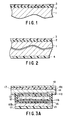
- FIG. 1 shows a cross-sectional view of one example of the reflection preventive optical member according to this invention.
- a reflection preventive film 2 is deposited on one of the surfaces of a transparent substrate 1. Further, an anti-smudge layer 3 is formed on this reflection preventive film 2 according to the method of this invention.
- This reflection preventive optical member according to this invention is then adhered to a functional optical member such as a polarizing plate by a suitable bonding method such as lamination thereby to obtain an optical functional member of this invention exhibiting a reflection preventive function.
- FIG. 2 shows a cross-sectional view of one example of the optical functional member according to this invention.
- a reflection preventive film 2 is deposited on one of the surfaces of a transparent substrate 1. Further, an anti-smudge layer 3 is formed on this reflection preventive film 2 according to the method of this invention. Further, a polarizing plate 4 acting as a functional optical member is formed on the other surface of the transparent substrate 1.
- This reflection preventive optical member or an optical functional member laminated with this reflection preventive optical member is then adhered, by making use of an adhesive or a pressure-sensitive adhesive, onto the front face plate (a glass plate, a plastic plate or a polarizing plate) of various display devices (a liquid crystal display, a CRT display, a projection television, a plasma display, an EL display, etc.) thereby to obtain a display device of this invention.
- an adhesive or a pressure-sensitive adhesive onto the front face plate (a glass plate, a plastic plate or a polarizing plate) of various display devices (a liquid crystal display, a CRT display, a projection television, a plasma display, an EL display, etc.) thereby to obtain a display device of this invention.
- FIG. 3 shows a schematical view of one example of the display device according to this invention.
- a TFT substrate 10a provided on one surface thereof with an alignment film lla is disposed to face a glass substrate 10b provided on one surface thereof with an alignment film 11b with a spacer 13 being interposed therebetween.
- a liquid crystal layer 12 is kept sustained between the TFT substrate 10a and the glass substrate 10b.
- the TFT substrate 10a is provided with a display electrode 14, and the glass substrate 10b is provided with a color filter 15 and a counter electrode 16.
- a polarizing plate 17 is formed on the other surface of each of the TFT substrate 10a and the glass substrate 10b.
- An optical functional member 18 provided with an anti-smudge layer which has been formed using an anti-smudge agent of this invention is formed on the surface of the polarizing plate 17 formed on the TFT substrate 10a.
- FIG. 3B shows a schematical view of a portion of a CRT display.
- an optical functional member 22 provided with an anti-smudge layer which has been formed using an anti-smudge agent of this invention is formed on the surface of a panel 21.
- an anti-smudge layer is formed on the surface of an optical functional member so as to prevent a smudge such as fingerprints, skin fat, sweat, cosmetics, etc. from adhering onto the surface of an optical functional member.
- This anti-smudge layer is excellent in durability and capable of easily wiping off a smudge even if the smudge is adhered onto the surface of the anti-smudge layer. Therefore, it is possible to obtain a display device which is excellent in image recognizability.
- a reflection preventive film-attached TAC (triacetyl cellulose)film was prepared as follows.
- a monofunctional acrylic resin was coated on the surface of a TAC film (thickness: 80 ⁇ m) by means of a microgravure method. Then, the light from a metahalide lamp (120W) was irradiated to the coated layer from a distance of 20 cm for 10 seconds, thereby forming a hard coat layer. Thereafter, a first TiO 2 film, a first SiO 2 film, a second TiO 2 film and a second SiO 2 film successively deposited on the hard coat layer by means of a plasma assist deposition method, thereby obtaining a reflection preventive layer.
- the optical film thickness was watched by making use of an optical film thickness monitor, and when an aimed quantity of light was reached, the operation of forming the film was stopped thereby to obtain a predetermined optical film thickness.
- the reflection preventive film-attached TAC films obtained in this manner were employed as a treating substrate or as a transparent substrate for forming an anti-smudge layer.
- the mixture was allowed to react while being heated at reflux for 10 hours, thereby obtaining an organosilicon compound.
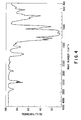
- this organosilicon compound was subjected to an FT-IR analysis to obtain an FT-IR chart as shown in FIG. 4.
- the organosilicon compound thus obtained was diluted with perfluorohexane to a 0.1 wt% solution thereby obtaining an anti-smudge agent of this invention.
- the reflection preventive film-attached TAC film prepared as mentioned above was employed as a treating substrate, and the anti-smudge agent obtained in this example was coated on the surface of the treating substrate by means of a dip coating method.
- the coated substrate was then heat-dried at a temperature of 60°C for one minute thereby to form an anti-smudge layer, thereby obtaining a reflection preventive optical member of this example.
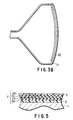
- FIG. 5 shows a cross-sectional view of the reflection preventive optical member obtained in this manner.
- the reflection preventive optical member according to this example was constructed such that a hard coat layer 5 was formed on a transparent substrate 1, and a reflection preventive film 2 formed of a laminate structure consisting of a first TiO 2 film 2a, a first SiO 2 film 2b, a second TiO 2 film 2c and a second SiO 2 film 2d was deposited on the surface of hard coat layer 5.
- the uppermost layer of this optical member was constituted by an anti-smudge layer 3 formed from the anti-smudge agent of this invention.
- the organosilicon compound obtained in Example 1 and represented by the chemical formula (6) was diluted with perfluorohexane to a 20 wt% solution thereby obtaining an anti-smudge agent of this example.
- the reflection preventive film-attached TAC film prepared as mentioned above was employed as a treating substrate, and the anti-smudge agent obtained in this example was deposited on the surface of the treating substrate by means of a vacuum deposition method (resistance heating method), thereby forming an anti-smudge layer.
- Example 2 The same procedures as those of Example 2 were repeated except that CF 3 (CF 2 ) 7 (CH 2 ) 2 Si(NH) 3/2 (KP801M; Shin-etsu Chemical Industries Ltd.) was employed as an anti-smudge agent, thereby forming an anti-smudge layer on the surface of a treating substrate.
- CF 3 (CF 2 ) 7 (CH 2 ) 2 Si(NH) 3/2 KP801M; Shin-etsu Chemical Industries Ltd.
- a pellet having a diameter of 6 mm and a height of 4 mm was manufactured by means of hydraulic press and by making use of Al 2 O 3 powder having a particle diameter of 1 to 10 ⁇ m as a raw material. Then, this pellet was sintered at a temperature of 1,200°C for 14 hours. The resultant sintered substance (pellet) was found as having a porosity of about 40%.
- sodium hydride oil suspension was placed in a 100 mL two-necked eggplant type flask provided with a dropping funnel and a reflux condenser thereby to perform nitrogen displacement. After this displacement, the washing with n-hexane under nitrogen gas atmosphere was repeated four times, and then n-hexane was distilled in vacuum thereby to obtain sodium hydride (0.011 mol).
- a fluorine resin having hydroxyl group and represented by the following chemical formula (4) was dissolved in 50g of bis(trifluoromethyl) benzene to prepare a solution.
- the resultant solution was then gently dropped under ice-cooling into the flask at a rate of one drop per second. After finishing this dropping operation, the reaction mixture was taken out of the ice bath and stirred for 10 hours at room temperature.
- 0.1 mol of chloromethyltrimethoxy silane represented by the following formula (7) was added to sodium alkoxide and the resultant mixture was stirred for two hours at room temperature. Thereafter, the reaction mixture was heated at reflux for 72 hours while maintaining the heating temperature at 90°C.
- the organosilicon compound represented by the aforementioned formula (8) was diluted with perfluorohexane to a 10 wt% solution thereby obtaining an anti-smudge agent.
- the aforementioned porous molded body (pellet) was dipped into the anti-smudge agent solution so as to completely saturate the porous molded body with the anti-smudge agent.
- the porous molded body was taken out of the anti-smudge agent solution, and the solvent was allowed to evaporate.
- the porous molded body (pellet) was found as containing about 2 wt% of the anti-smudge agent.
- the pellet was mounted on a molybdenum boat, and the anti-smudge agent was allowed to deposit on the aforementioned reflection preventive film-attached TAC film by means of a vacuum deposition method (resistance heating method) thereby to form an anti-smudge layer.
- a vacuum deposition method resistance heating method
- the interior of the deposition apparatus was evacuated to a vacuum degree of 5 ⁇ 10 -5 torr or less. Thereafter, the boat was heated to 400°C so as to evaporate the anti-smudge agent.
- Example 3 The same procedures as those of Example 3 were repeated except that CF 3 (CF 2 ) 7 (CH 2 ) 2 Si(NH) 3/2 (KP801M; Shin-etsu Chemical Industries Ltd.) was employed as an anti-smudge agent, thereby forming an anti-smudge layer on the surface of the reflection preventive film-attached TAC film.
- CF 3 (CF 2 ) 7 (CH 2 ) 2 Si(NH) 3/2 KP801M; Shin-etsu Chemical Industries Ltd.
- a pellet having a porosity of about 40% was prepared in the same procedures as those of Example 3.
- sodium hydride oil suspension was placed in a 100 mL two-necked eggplant type flask provided with a dropping funnel and a reflux condenser thereby to perform nitrogen displacement. After this displacement, the washing with n-hexane under nitrogen gas atmosphere was repeated four times, and then n-hexane was distilled in vacuum thereby to obtain sodium hydride (0.011 mol).
- a fluorine resin having hydroxyl group and represented by the following chemical formula (4) was dissolved in 50g of bis(trifluoromethyl) benzene to prepare a solution.
- the resultant solution was then gently dropped under ice-cooling into the flask at a rate of one drop per second. After finishing this dropping operation, the reaction mixture was taken out of the ice bath and stirred for 10 hours at room temperature.
- 0.03 mol of chloromethyltrimethoxy silane represented by the following formula (7) was added to sodium alkoxide and the resultant mixture was stirred for two hours at room temperature. Thereafter, the reaction mixture was heated at reflux for 48 hours while maintaining the heating temperature at 100°C.
- the organosilicon compound represented by the aforementioned formula (9) was diluted with perfluorohexane to a 10 wt% solution thereby obtaining an anti-smudge agent.
- the aforementioned porous molded body (pellet) was dipped into the anti-smudge agent solution so as to completely saturate the porous molded body with the anti-smudge agent.
- the porous molded body was taken out of the anti-smudge agent solution, and the solvent was allowed to evaporate.
- the porous molded body (pellet) was found as containing about 2 wt% of the anti-smudge agent.
- the anti-smudge layer formed on the surface of an optical member by making use of an anti-smudge agent of this invention is capable of more effectively preventing smudges formed of fingerprints, skin fat, sweat, cosmetics, etc. from being adhered onto the surface thereof without deteriorating the optical properties of the optical member as compared with the anti-smudge layer formed by making use of the conventional anti-smudge agents, and even if a smudge is adhered to the anti-smudge layer, the smudge can be easily removed, and at the same time, the durability of anti-smudge property of the anti-smudge layer of this invention is excellent.
- an anti-smudge layer is to be formed by means of a wet coating method using an anti-smudge agent of this invention, it becomes possible to apply it to a treating substrate of complicated configuration and of large surface area, which the conventional dry coating method has failed to apply.
- an anti-smudge layer is to be formed by means of a dry coating method using an anti-smudge agent of this invention, the employment of a diluent solvent for the formation of an anti-smudge layer can be dispensed with, and at the same time, it becomes possible to precisely control the film thickness of the anti-smudge layer.
- a vacuum deposition method is employed by making use of a porous molded body for the formation of an anti-smudge layer, the controlling of film thickness would become more easy, thus being advantageous in the formation of the anti-smudge layer.
- the optical functional member of this invention that can be obtained by the lamination of an optical member or a reflection preventive optical member of this invention with a functional optical member such as a polarizing plate is provided on the surface thereof with an anti-smudge layer which is excellent in anti-smudge property as well as in durability, it is possible to obtain a display device which is excellent in image recognizability, if this optical functional member is attached to the front face of display screen of various display devices (such as a liquid crystal display, a CRT display, a projection television, a plasma display, an EL display, etc.).
- various display devices such as a liquid crystal display, a CRT display, a projection television, a plasma display, an EL display, etc.
- An anti-smudge agent characterized by containing an organosilicon compound represented by the following general formula (1): R f2 -(OC 3 F 6 ) n2 -O-(CF 2 ) m2 -(CH 2 ) 12 -Z-(CH 2 ) s2 -Si-(R 2 ) 3 wherein R f2 is a linear or branched perfluoroalkyl group having 1 to 16 carbon atoms; R 2 is a hydrolytic group; Z is -OOCNH- or -O-; n2 is an integer of 1 to 50; m2 is an integer of 0 to 3; 12 is an integer of 0 to 3; and s2 is an integer of 1 to 6, with a proviso that these m2 and 12 meet the condition of 6 ⁇ m2+12>0.
- organosilicon compound represented by the following general formula (1): R f2 -(OC 3 F 6 ) n2 -O-(CF 2 ) m2 -
Abstract
Description
- This invention relates to an anti-smudge agent for forming an anti-smudge layer on the surface of various kinds of substrate to be treated (hereinafter referred to simply as a treating substrate) and requiring an anti-smudge property, and to a method of forming an anti-smudge layer by making use of this anti-smudge agent. Additionally, this invention relates to an anti-reflection optical member which is adapted to be applied to the surface of display screen of an optical member (such as an anti-reflection film, an optical filter, an optical lens, spectacle lens, beam splitter, prism, mirror, etc.) and a device (such as a liquid crystal display, a CRT display, a projection television, a plasma display, an EL display, etc.), to an optical functional member, and to a display device wherein this optical functional member is adhered to the surface of display screen of the display device.
- Optical members such as an anti-reflection film, an optical filter, an optical lens, spectacle lens, beam splitter, prism, mirror, etc. are liable to be soiled with smudges originating from fingerprints, skin fat, sweat, cosmetics, etc. as these members are employed by an operator. Once these members are soiled with these smudges, it is very difficult to remove them. Particularly in the case of an optical member provided with an antireflection coating, the smudge adhered to the antireflection coating stands out from the coating, thus raising a problem.
- Meanwhile, most of display devices are generally employed under the condition that external light enters freely into the display screen from the inside as well as outside of the room.
- The incident light like this external light is mirror-reflected by the surface of the display screen, thus causing a mixing of images between the reflected image and the displayed image, resulting in the deterioration of the display quality and hence the blurring of the display image.
- In particular, since the frequency of using a computer has been recently increased with an progress of office automation, and hence the time during which an operator stares at the display screen has been also increased recently, the deterioration of display quality due to the reflection image is now considered as being one of the causes for bringing about a health hazard such as the fatigue of eyes.
- Furthermore, with an increasing popularization of out-door life in recent years, the opportunity of using various kinds of display device outside the door is increasing now. As a result, it is now demanded to improve the quality of display so as to enable a display image to be recognized more clearly.
- With a view to meet these demands, there has been conventionally proposed an idea of attaching a reflection preventive optical member to the surface of the display screen, this reflection preventive optical member being capable of preventing the reflection of light over a wide range of visible light. One example of such a reflection preventive optical member is a laminate film comprising a transparent substrate on the surface which a high refractive index layer and a low refractive index layer both consisting of a metal oxide are laminated. There is also known a reflection preventive optical member which is formed of a laminate film comprising a transparent substrate on the surface which a low refractive index layer consisting of an inorganic or organic fluorine compound is laminated.
- On the other hand, it is also known that the same effect as that of a reflection preventive optical member can be obtained by the employment of an irregular reflective film comprising a transparent plastic film substrate on the surface of which a coating layer containing transparent fine particles is deposited to form a rugged surface so as to cause the external light to be irregularly reflected by the rugged surface.
- In the meantime, the aforementioned reflection preventive optical members tend to be soiled with smudges originating from fingerprints, skin fat, sweat, cosmetics, etc. as the display device provided with this reflection preventive optical member is employed by an operator. Specifically, since the surface energy of the reflection preventive film is generally as large as 60 J/m2 or so, the reflection preventive film is more likely to be soiled with these smudges. Further, since the surface of the reflection preventive film is constituted by a finely roughened surface, once these smudges are adhered onto the reflection preventive film, it is very difficult to remove them. Further, there is also a problem that when these smudges are adhered to a portion of the reflection preventive film, the soiled portion becomes more reflective, thereby rendering the soiled portion to stand out from the remaining portion.
- With a view to solve this problem of the smudge on the surface of reflection preventive optical member, various techniques for forming an anti-smudge layer which is capable of preventing smudges from adhering thereon and capable of easily removing the adhered smudges have been proposed up to date.
- Japanese Patent Unexamined Publication S64-86101 teaches a reflection preventive article having anti-smudge and abrasion resistive properties wherein the surface of the substrate is covered with a reflection preventive film consisting mainly of silicon dioxide, and the resultant surface is further treated with a compound containing an organosilicic substituent group. Japanese Patent Unexamined Publication H4-338901 teaches a CRT filter having anti-smudge and abrasion resistive properties, whose substrate surface is covered with a terminal silanol organopolysiloxane. Japanese Patent Publication H6-29332 teaches an anti-smudge/low reflectance plastic covered on its surface with a refection preventive film containing mono- and di-silane compounds containing polyfluoroalkyl group, and a silanized halogen, alkyl or alkoxy compound. Further, Japanese Patent Unexamined Publication H7-16940 teaches an optical member comprising an optical thin film consisting mainly of silicon dioxide, on which a copolymer consisting of perfluoroalkyl(meta)acrylate and a monomer having alkoxy silane group is formed.
- However, the anti-smudge layer manufactured according to these conventional methods is insufficient in anti-smudge property, incapable of allowing a smudge such as fingerprints, skin fat, sweat, cosmetics, etc. to be easily removed therefrom, and poor in durability losing sharply its anti-smudge property with a repetition of use. Therefore, it is now desired to develop an anti-smudge layer which is excellent in anti-smudge property and in the durability of anti-smudge property.
- This invention has been made to overcome the aforementioned conventional problems, and therefore, an object of this invention is to provide an anti-smudge agent, which makes it possible to obtain an anti-smudge layer which is excellent in durability of the property, capable of preventing smudges formed of fingerprints, skin fat, sweat, cosmetics, etc. from being adhered onto the surface of an optical member such as a reflection preventive film, and capable of allowing these smudges to be easily removed even if these smudges are adhered onto the optical member.
- Another object of this invention is to provide a method of forming an anti-smudge layer which is capable of easily forming an anti-smudge layer which is excellent in anti-smudge property and in the durability of the anti-smudge property.
- Still another object of this invention is to provide a optical member which is provided with the aforementioned anti-smudge layer.
- Still another object of this invention is to provide a reflection preventive optical member which is provided with the aforementioned anti-smudge layer.
- A further object of this invention is to provide an optical functional member which is provided with the aforementioned reflection preventive optical member.
- A still further object of this invention is to provide a display device whose display screen surface is constituted by the aforementioned optical functional member.
- According to this invention, there is provided an anti-smudge agent containing an organosilicon compound represented by the following general formula (1):
- According to this invention, there is provided an anti-smudge agent containing an organosilicon compound represented by the following general formula (3):wherein Rf2 is a linear or branched perfluoroalkyl group having 1 to 16 carbon atoms; R3 is an alkyl group having 1 to 10 carbon atoms; X is a halogen atom; n2 is an integer of 1 to 50; m2 is an integer of 0 to 3; 12 is an integer of 0 to 3; and s2 is an integer of 1 to 6; a is an integer of 0 to 3; b is an integer of 0 to 3; c is 0 or 1; d is 0 or 1; with a proviso that these m2, 12, a, b, c and d meet the conditions of 6≧m2+12>0, a+b=3, and c+d=1.

- According to this invention, there is further provided a method of forming an anti-smudge layer containing the aforementioned anti-smudge agent.
- According to this invention, there is further provided an optical member provided with an anti-smudge layer containing the aforementioned anti-smudge agent.
- According to this invention, there is further provided a reflection preventive optical member provided with an anti-smudge layer containing the aforementioned anti-smudge agent.
- According to this invention, there is further provided an optical functional member constituted by the aforementioned reflection preventive optical member.
- According to this invention, there is further provided a display device provided with the aforementioned optical functional member.
- This summary of the invention does not necessarily describe all necessary features so that the invention may also be a sub-combination of these described features.
- The invention can be more fully under stood from the following detailed description when taken in conjunction with the accompanying drawings, in which:
- FIG. 1 is a cross-sectional view illustrating the structure of one example of reflection preventive optical member according to this invention;
- FIG. 2 is a cross-sectional view illustrating the structure of one example of optical functional member according to this invention;
- FIGS. 3A and 3B are schematical views each illustrating the structure of one example of display device according to this invention;
- FIG. 4 is an FT-IR chart of an organosilicon compound constituting an anti-smudge agent according to this invention; and
- FIG. 5 is a cross-sectional view illustrating the structure of another example of reflection preventive optical member according to this invention.
-
- The anti-smudge agent according to this invention is characterized in that it contains a specific kind of organosilicon compound. As a result, when an anti-smudge layer is formed on the surface of a treating substrate by making use of this anti-smudge agent, it is possible, if the treating substrate is any kind of optical members such as an anti-reflection film, an optical filter, an optical lens, spectacle lens, beam splitter, prism, mirror, etc., to prevent smudges formed any of fingerprints, skin fat, sweat, cosmetics, etc. from being adhered onto the surface of these optical members, and furthermore, to easily remove these smudges adhered onto these optical members without deteriorating the optical properties of these optical members. Moreover, the anti-smudge layer formed by making use of this anti-smudge agent is excellent in durability of the property.
- Namely, the anti-smudge agent according to this invention contains an organosilicon compound represented by the following general formula (1):
- The number of carbon atom of the linear or branched perfluoroalkyl group to be introduced into Rf2 is preferably in the range of from 1 to 16, more preferably in the range of from 1 to 3. Therefore, most preferable examples of Rf2 are -CF3, -C2F5, -C3F7, etc.
- Specific examples of the hydrolytic group to be introduced into R2 are -Cl, -Br, -I, -OR11, -OOCR11, -OC(R11)C=C(R12)2, -ON=C(R11)2, -ON=CR13, -N(R12)2, -R12NOCR11, etc., wherein R11 is an aliphatic hydrocarbon group having 1 to 10 carbon atoms such as alkyl group or an aromatic hydrocarbon group having 6 to 20 carbon atoms such as phenyl group; R12 is hydrogen atom or an aliphatic hydrocarbon group having 1 to 5 carbon atoms such as alkyl group; and R13 is a bivalent aliphatic hydrocarbon group having 3 to 6 carbon atoms such as alkylidene.
- Most preferable examples of the hydrolytic group are -OCH3, -OC2H5, -OOCCH3, and -NH2.
- These hydrolytic groups may be included singly or in combination of two or more kinds in the organosilicon compound constituting the anti-smudge agent of this invention.
- The n2 in the aforementioned general formula (1) should preferably be in the range of 1 to 30, more preferably in the range of 5 to 20. The m2 in the aforementioned general formula (1) should preferably be in the range of 1 to 2. The 12 in the aforementioned general formula (1) should preferably be in the range of 1 to 2. The s2 in the aforementioned general formula (1) should preferably be in the range of 1 to 3.
- The compounds where Z is -OOCNH- in the general formula (1) may be prepared according to the following reaction formula:

- More specifically, an organosilicon compound represented by the following general formula (2D) can be obtained by allowing a fluorine resin having hydroxyl group and represented by the following general formula (2A) to react with catalyst and a isocyanate-based silane coupling agent represented by the following general formula (2C) in a solvent.
- This reaction can be advantageously proceeded by using 0.001 to 0.01 mol of C32H64O4Sn as a catalyst and 1 to an excess of a isocyanate-based silane coupling agent per 1 mol of a fluorine resin containing hydroxyl group and by performing the reaction at a temperature ranging from room temperature to the reflux temperature of the solvent for 2 to 72 hours. As for the solvent useful in this case, it is possible to employ an ordinary perfluoroaliphatic hydrocarbon having 5 to 12 carbon atoms, such as perfluorohexane, perfluoromethylcyclohexane, perfluoro-1,3-dimethylcyclohexane, etc.; an aromatic hydrocarbon polyfluoride such as bis(trifluoromethyl) benzene; or an aliphatic hydrocarbon polyfluoride.
- The anti-smudge agent according to this invention may include, if desired, various kinds of additives in addition to the aforementioned organometallic compounds represented by the general formula (1). For example, the anti-smudge agent may contain a catalyst for promoting the hydrolysis or polycondensation of the organosilicon compounds represented by the general formula (1) or for promoting the formation of condensed urethane linkage.
- As to the catalyst that can be employed in the anti-smudge agent of this invention, it is possible to employ hydrochloric acid, nitric acid, sulfuric acid, acetic acid, hydrofluoric acid, formic acid, phosphoric acid, oxalic acid, ammonia, aluminum acetylacetonate, dibutyltin dilaurate, octylate tin compound, sodium, sodium hydride, methane sulfonate, trifluoromethane sulfonate, paratoluene sulfonate, trifluoroacetate, etc. These compounds can be employed singly or in combination of two or more kinds.
- The compounds where Z is -O- in the general formula (1) may be prepared according to the following reaction formula:

- More specifically, an organosilicon compound represented by the following general formula (2E) can be obtained by allowing a fluorine resin having hydroxyl group and represented by the following general formula (2A) to react with catalyst and a halogen-based silane coupling agent represented by the following general formula (2B) in a solvent.
- This reaction can be advantageously proceeded by using 1 to 1.1 excess of NaH as a catalyst and 1 to an excess of a halogen-based silane coupling agent per 1 mol of a fluorine resin containing hydroxyl group and by performing the reaction at a temperature ranging from room temperature to the reflux temperature of the solvent for 2 to 72 hours. As for the solvent useful in this case, it is possible to employ an ordinary perfluoroaliphatic hydrocarbon having 5 to 12 carbon atoms, such as perfluorohexane, perfluoromethylcyclohexane, perfluoro-1,3-dimethylcyclohexane, etc.; an aromatic hydrocarbon polyfluoride such as bis(trifluoromethyl) benzene; or an aliphatic hydrocarbon polyfluoride.
- The anti-smudge agent according to this invention may include, if desired, various kinds of additives in addition to the aforementioned organometallic compounds represented by the general formula (1). For example, the anti-smudge agent may contain a catalyst for promoting the hydrolysis or polycondensation of the organosilicon compounds represented by the general formula (1) or for promoting the formation of condensed ether linkage.
- As to the catalyst that can be employed in the anti-smudge agent of this invention, it is possible to employ hydrochloric acid, nitric acid, sulfuric acid, acetic acid, hydrofluoric acid, formic acid, phosphoric acid, oxalic acid, ammonia, aluminum acetylacetonate, dibutyltin dilaurate, octylate tin compound, sodium, sodium hydride, methane sulfonate, trifluoromethane sulfonate, paratoluene sulfonate, trifluoroacetate, etc. These compounds can be employed singly or in combination of two or more kinds.
- Another example of the organosilicon compound constituting the anti-smudge agent is an organosilicon compound represented by the following general formula (3):wherein Rf2 is a linear or branched perfluoroalkyl group having 1 to 16 carbon atoms; R3 is an alkyl group having 1 to 10 carbon atoms; X is a halogen atom; n2 is an integer of 1 to 50; m2 is an integer of 0 to 3; 12 is an integer of 0 to 3; and s2 is an integer of 1 to 6; a is an integer of 0 to 3; b is an integer of 0 to 3; c is 0 or 1; d is 0 or 1; with a proviso that these m2, 12, a, b, c and d meet the conditions of 6≧m2+12>0, a+b=3, and c+d=1.

- The number of carbon atom of the linear or branched perfluoroalkyl group to be introduced into Rf2 is preferably in the range of from 1 to 16, more preferably in the range of from 1 to 3. Therefore, most preferable examples of Rf2 are -CF3, -C2F5, -C3F7, etc.
- The number of carbon atom of the alkyl group to be introduced into R3 is preferably in the range of from 1 to 10, more preferably in the range of from 1 to 3. Therefore, most preferable examples of R3 are -CH3, -C2H5, -C3H7, etc.
- The compounds represented the general formula (3) may be prepared according to the following reaction formula:

- More specifically, an organosilicon compound represented by the following general formula (3) can be obtained by allowing a fluorine resin having hydroxyl group and represented by the following general formula (3A) to react with catalyst and a halogen-based silane coupling agent represented by the following general formula (3B) in a solvent.wherein Rf2 is a linear or branched perfluoroalkyl group having 1 to 16 carbon atoms; R3 is an alkyl group having 1 to 10 carbon atoms; X is a halogen atom; n2 is an integer of 1 to 50; m2 is an integer of 0 to 3; 12 is an integer of 0 to 3; and s2 is an integer of 1 to 6; a is an integer of 0 to 3; b is an integer of 0 to 3; c is 0 or 1; d is 0 or 1; with a proviso that there m2, 12, a, b, c and d meet the conditions of 6≧m2+m2>0, a+b=3, c+d=1.
- This reaction can be advantageously proceeded by using 1 to 1.1 excess of NaH as a catalyst and 1 to an excess of a halogen-based silane coupling agent per 1 mol of a fluorine resin containing hydroxyl group and by performing the reaction at a temperature ranging from room temperature to the reflux temperature of the solvent for 2 to 72 hours. As for the solvent useful in this case, it is possible to employ an ordinary perfluoroaliphatic hydrocarbon having 5 to 12 carbon atoms, such as perfluorohexane, perfluoromethylcyclohexane, perfluoro-1,3-dimethylcyclohexane, etc.; an aromatic hydrocarbon polyfluoride such as bis(trifluoromethyl) benzene; or an aliphatic hydrocarbon polyfluoride.
- These organosilicon compounds represented by the aforementioned general formula (3) can be employed singly or in combination of two or more kinds for constituting the anti-smudge agent of this invention. When a mixture comprising plural kinds of these silane compounds is to be employed, the components "a", "b", "c" and "d" in the aforementioned general formula (3) should be differentiated.
- The anti-smudge agent according to this invention may include, if desired, various kinds of additives in addition to the aforementioned organometallic compounds represented by the general formula (3). For example, the anti-smudge agent may contain a catalyst for promoting the hydrolysis or polycondensation of the organosilicon compounds represented by the general formula (3) or for promoting the formation of condensed ether linkage.
- As to the catalyst that can be employed in the anti-smudge agent of this invention, it is possible to employ hydrochloric acid, nitric acid, sulfuric acid, acetic acid, hydrofluoric acid, formic acid, phosphoric acid, oxalic acid, ammonia, aluminum acetylacetonate, dibutyltin dilaurate, octylate tin compound, sodium, sodium hydride, methane sulfonate, trifluoromethane sulfonate, paratoluene sulfonate, trifluoroacetate, etc. These compounds can be employed singly or in combination of two or more kinds.
- As for the treating substrate to which an anti-smudge layer is applied by making use of the anti-smudge agent of this invention, there is not any particular restriction, i.e. an ordinary optical member is applicable. For example, an inorganic substrate such as a glass board, a glass board comprising an inorganic compound layer; or an organic substrate such as a transparent plastic substrate, a transparent plastic substrate comprising an inorganic compound layer can be employed.
- Among them, a glass board may be mainly employed as an inorganic substrate. As for the inorganic compound to be employed for constituting the glass board comprising an inorganic compound layer, it is possible to employ a metal oxide such as silicon oxide (silicon dioxide, silicon monooxide, etc.), aluminum oxide, magnesium oxide, titanium oxide, tin oxide, zirconium oxide, sodium oxide, antimony oxide, indium oxide, bismuth oxide, yttrium oxide, cerium oxide, zinc oxide, ITO (indium tin oxide), etc.; or a metal halide such as magnesium fluoride, calcium fluoride, sodium fluoride, lanthanum fluoride, cerium fluoride, lithium fluoride, thorium fluoride, etc.
- The inorganic substrate or inorganic compound layer formed of any of these inorganic compounds may be of a single layer or a multi-layer. The inorganic compound layer functions as a reflection preventive layer and can be formed by making use of any conventional method such as a wet coating method, a PVD (Physical Vapor Deposition) method and a CVD (Chemical Vapor Deposition) method. The wet coating method may be a dip coating method, a spin coating method, a flow coating method, a spray coating method, a roll coating method, a gravure coating method, etc. As for the PVD method, it is possible to employ a vacuum deposition method, a reactive vapor deposition method, an ion beam assist method, a sputtering method, an ion plating method, etc.
- As for the transparent plastic substrate which is one example of an organic substrate to be employed as a treating substrate, various kinds of organic polymer substrates may be employed. The materials to be employed as an optical member are generally required to be excellent not only in optical properties such as transparency, refractive index and dispersivity, but also in other physical properties such as shock resistance, heat resistance and durability. In view of these requirements, a polyolefin resin (polyethylene, polypropylene, etc.), a polyester resin (polyethylene terephthalate, polyethylene naphthalate, etc.), a polyamide resin (nylon-6, nylon-66, etc.), polystyrene, polyvinyl chloride, polyimide, polyvinyl alcohol, ethylene vinyl alcohol, acrylic resin, cellulose (triacetyl cellulose, diacetyl cellulose, cellophane, etc.), or a copolymer of these organic polymer may be employed. Therefore, these polymer can be employed also in this invention as a transparent plastic substrate for constituting the treating substrate.
- It is also possible to incorporate various kinds of conventional additives such as an anti-static agent, an ultraviolet absorbent, a plasticizer, a lubricant, a colorant, an antioxidant, a flame retardant, etc. into the organic polymer constituting these organic substrates.
- An inorganic compound layer may be superimposed on these organic substrates to be employed as the treating substrate in this invention. In this case, the inorganic compound layer functions as a reflection preventive layer, and can be deposited on the surface of the organic substrates in the same manner as explained above.
- There is not any particular limitation regarding the shape of the inorganic substrate or organic substrate to be employed as the treating substrate. The transparent plastic substrate to be employed as an optical member is generally provided in the form of film or sheet, and hence, a film-like or sheet-like transparent plastic substrate can be employed in this invention also. This film-like or sheet-like transparent plastic substrate may be formed of a single layer or of a laminate layer consisting of plural organic polymer layers. Although there is not any particular limitation regarding the thickness of the transparent plastic substrate, the thickness should preferably be in the range of 0.01 to 5 mm.
- It is also possible to interpose a hard coat layer between the transparent plastic substrate and the inorganic compound layer. The provision of this hard coat layer is effective in improving not only the hardness of the substrate surface but also the adhesivity between the transparent plastic substrate and the inorganic compound layer, since the flatness of the substrate surface can be improved by this hard coat layer. Therefore, any scratch that may be caused by the pressing of pencil, etc. on the substrate surface can be effectively prevented. Moreover, the generation of cracks of the inorganic compound layer due to the bending of the transparent plastic substrate can be effectively prevented, thus making it possible to improve the mechanical strength of the optical member.
- There is not any particular limitation with regard to the material of the hard coat layer as long as the hard coat layer is excellent in transparency, sufficient in hardness and excellent in mechanical strength. For example, a cured resin which can be cured by the irradiation of an ionizing radiation or ultraviolet ray, or a thermosetting resin can be employed. In particular, an ultraviolet irradiation-curing type acrylic resin, an organic silicone resin and a thermosetting type polysiloxane resin are preferable for forming the hard coat layer. It is more preferable that the refractive index of these resins is the same or nearly the same as that of the transparent plastic substrate.
- There is not any particular limitation with regard to the method of coating the hard coat layer as long as it is capable of forming a uniform layer. The thickness of the hard coat layer may be sufficient if it is 3 µm or more for ensuring a sufficient strength. In view of the transparency, coating precision and handling thereof however, a preferable range in thickness of the hard coat layer is 5 to 7 µm.
- It is also possible to mix and disperse an inorganic or organic fine particle having an average particle diameter of 0.01 to 3 µm into the hard coat layer, thereby achieving a light dispersion treatment or so-called anti-glare treatment. Although there is not any particular limitation regarding this inorganic or organic fine particle as long as the fine particle is transparent, it is more preferable to employ a material of low refractive index. Specifically, silicon oxide and magnesium fluoride is especially preferable in view of the stability and heat resistance thereof. The aforementioned light dispersion treatment can be realized also by roughening the surface of the hard coat layer.
- The aforementioned treating substrate can be employed as a transparent substrate for the reflection preventive member in this invention. In particular, the treating substrate provided on its surface with a reflection preventive film can be treated in this invention as a transparent substrate provided with a reflection preventive film. The reflection preventive optical member according to this invention can be obtained by depositing an anti-smudge layer on the surface of the aforementioned resultant transparent substrate.
- As for the method of forming the anti-smudge layer, there is not any particular limitation, and hence it is possible to adopt either a wet coating method or a dry coating method.
- This wet coating method may be a dip coating method, a spin coating method, a flow coating method, a spray coating method, a roll coating method, a gravure coating method, etc.
- On the other hand, the dry coating method may be for instance a vacuum deposition method, a sputtering method or a CVD method. More specifically, the vacuum deposition method may be performed by way of a resistance heating method, an electron beam method, a high frequency heating method, an ion beam method, etc. The CVD method can be performed by way of a plasma CVD method, a light CVD method, a thermal CVD method, etc.
- Although there is not any particular limitation regarding a diluent solvent to be employed in the wet coating method, it is preferable to employ a perfluoroaliphatic hydrocarbon having 5 to 12 carbon atoms such as perfluorohexane, perfluoromethylcyclohexane, perfluoro-1,3-dimethylcyclohexane; an aromatic hydrocarbon polyfluoride such as bis(trifluoromethyl) benzene; and an aliphatic hydrocarbon polyfluoride. These solvents may be employed singly or as a mixture containing two or more kinds of these solvents.
- The employment of this wet coating method is preferable where the treating substrate is of complicated configuration or large in surface area.
- On the other hand, the employment of dry coating method which can be dispensed with the employment of a diluent solvent is preferable in view of the working environment at the occasion of forming an anti-smudge layer or in view of controlling the film thickness of an anti-smudge layer. In that respect, the employment of a vacuum deposition method is most preferable. It is possible according to a dry coating method to precisely control the film thickness of the anti-smudge layer to the order of angstrom which the prior art has failed to achieve so far. As a result, it is now possible to provide an optical member having a desired anti-smudge layer. Further, it is now possible to easily provide an optical member having a reflection preventive film with an anti-smudge property without causing any change in interference color of the reflection preventive film where the color is difficult to set.
- By the way, in the case where an anti-smudge layer is to be formed by means of a dry coating method, the film thickness to be formed changes depending on the quantity of evaporation of the anti-smudge agent. Therefore, if the film thickness of an anti-smudge layer is to be precisely controlled, the quantity of the evaporation of the anti-smudge agent should preferably be controlled precisely.
- After finishing the deposition of an anti-smudge layer on a treating substrate by means of a dry coating method or a wet coating method, the anti-smudge layer may be subjected, if desired, to heating, humidification, light irradiation, electron beam irradiation, etc.
- In particular, it is also preferable to form an anti-smudge layer by means of vacuum deposition method using a porous molded body.
- Namely, this vacuum deposition method comprises the steps of; impregnating a porous molded body with an anti-smudge agent of this invention; and heating the porous molded body impregnated with the anti-smudge agent in vacuum so as to evaporate the anti-smudge agent and to deposit an anti-smudge layer on a transparent substrate covered in advance with a reflection preventive film.
- As for the components constituting the porous molded body (pellet)to be employed in this method, it is possible to employ SiO2, TiO2, ZrO2, MgO, Al2O3, CaSO4, Cu, Fe, Al, stainless steel, carbon or a mixture thereof. Generally, these materials should be pulverized to have a particle diameter in the range of 5 to 20 µm. These pulverized materials are then pelletized and sintered according to the conventional method thereby obtaining a porous molded body to be employed in this invention.
- The sintering step of the pellet is generally performed at a temperature of 700 to 1,400°C for 1 to 10 hours. Depending on the particle diameter of the primary particle, density and sintering conditions, a porous molded body having a varied degree of porosity ranging from 30 to 60% can be obtained.
- The anti-smudge agent of this invention is dissolved in a solvent such as perfluorohexane to obtain a solution, into which the porous molded body (pellet) is dipped so as to completely saturate the porous molded body with the anti-smudge agent. Thereafter, the solvent is allowed to evaporate, thus obtaining a porous molded body impregnated with the anti-smudge agent of this invention.
- Then, by making use of this porous molded body impregnated with the anti-smudge agent, an anti-smudge layer is deposited on the surface of a treating substrate by means of a vacuum deposition method. As for the heating method for heating the porous molded body thereby to evaporate the anti-smudge agent, a resistance heating method, an electron beam heating method, ion beam heating method, high frequency heating method or a light heating method can be effectively employed.
- After finishing the deposition of an anti-smudge layer on the treating substrate, the resultant substrate may be subjected, if desired, to heating, humidification, light irradiation, electron beam irradiation.
- As explained above, if an anti-smudge layer is to be formed by means of a dry coating method, the quantity of the evaporation of the anti-smudge agent should preferably be controlled precisely in order to precisely control the film thickness of the anti-smudge layer. When the aforementioned porous molded body is employed, the evaporation quantity of the anti-smudge agent is determined by the impregnated quantity of the anti-smudge agent in the porous molded body and by the heating conditions at the occasion of forming the anti-smudge layer, and hence the employment of the porous molded body is advantageous in terms of controlling the film thickness. The employment of the porous molded body for forming an anti-smudge layer by means of a vacuum deposition method is also advantageous in the respects that preventing leaked anti-smudge agent due to heating from contaminate the inner portion of the apparatus and in the respects that decreasing the splash phenomenon of the anti-smudge agent.
- Although there is not any particular limitation with respect to the film thickness of the anti-smudge layer to be formed using an anti-smudge agent of this invention, the film thickness should preferably be in the range of 10 to 500 angstroms in view of anti-smudge property, abrasion resistance and optical performance of an optical member.
- FIG. 1 shows a cross-sectional view of one example of the reflection preventive optical member according to this invention.
- Referring to FIG. 1, a reflection preventive film 2 is deposited on one of the surfaces of a transparent substrate 1. Further, an anti-smudge layer 3 is formed on this reflection preventive film 2 according to the method of this invention.
- This reflection preventive optical member according to this invention is then adhered to a functional optical member such as a polarizing plate by a suitable bonding method such as lamination thereby to obtain an optical functional member of this invention exhibiting a reflection preventive function.
- FIG. 2 shows a cross-sectional view of one example of the optical functional member according to this invention.
- Referring to FIG. 2, a reflection preventive film 2 is deposited on one of the surfaces of a transparent substrate 1. Further, an anti-smudge layer 3 is formed on this reflection preventive film 2 according to the method of this invention. Further, a polarizing plate 4 acting as a functional optical member is formed on the other surface of the transparent substrate 1.
- This reflection preventive optical member or an optical functional member laminated with this reflection preventive optical member is then adhered, by making use of an adhesive or a pressure-sensitive adhesive, onto the front face plate (a glass plate, a plastic plate or a polarizing plate) of various display devices (a liquid crystal display, a CRT display, a projection television, a plasma display, an EL display, etc.) thereby to obtain a display device of this invention.
- FIG. 3 shows a schematical view of one example of the display device according to this invention. In the liquid crystal display shown in FIG. 3A, a TFT substrate 10a provided on one surface thereof with an alignment film lla is disposed to face a glass substrate 10b provided on one surface thereof with an alignment film 11b with a spacer 13 being interposed therebetween. Additionally, a liquid crystal layer 12 is kept sustained between the TFT substrate 10a and the glass substrate 10b. Further, the TFT substrate 10a is provided with a display electrode 14, and the glass substrate 10b is provided with a color filter 15 and a counter electrode 16. Further, a polarizing plate 17 is formed on the other surface of each of the TFT substrate 10a and the glass substrate 10b.
- An optical functional member 18 provided with an anti-smudge layer which has been formed using an anti-smudge agent of this invention is formed on the surface of the polarizing plate 17 formed on the TFT substrate 10a.
- FIG. 3B shows a schematical view of a portion of a CRT display. As shown in FIG. 3B, an optical functional member 22 provided with an anti-smudge layer which has been formed using an anti-smudge agent of this invention is formed on the surface of a panel 21.
- As shown in these FIGS. 3A and 3B, an anti-smudge layer is formed on the surface of an optical functional member so as to prevent a smudge such as fingerprints, skin fat, sweat, cosmetics, etc. from adhering onto the surface of an optical functional member. This anti-smudge layer is excellent in durability and capable of easily wiping off a smudge even if the smudge is adhered onto the surface of the anti-smudge layer. Therefore, it is possible to obtain a display device which is excellent in image recognizability.
- Next, this invention will be further explained with reference to specific examples, which are not intended to limit this invention.
- First of all, a reflection preventive film-attached TAC (triacetyl cellulose)film was prepared as follows.
- A monofunctional acrylic resin was coated on the surface of a TAC film (thickness: 80 µm) by means of a microgravure method. Then, the light from a metahalide lamp (120W) was irradiated to the coated layer from a distance of 20 cm for 10 seconds, thereby forming a hard coat layer. Thereafter, a first TiO2 film, a first SiO2 film, a second TiO2 film and a second SiO2 film successively deposited on the hard coat layer by means of a plasma assist deposition method, thereby obtaining a reflection preventive layer.
- The refractive index "n", geometrical thickness "d" and optical film thickness "nd" of each layer were set to: the TAC film (n=1.49), the hard coat layer (n=1.51, d=about 5 µm), the first TiO2 film (n=2.30, nd=60 nm), the first SiO2 film (n=1.46, nd=40 nm), the second TiO2 film (n=2.30, nd=110 nm) and the second SiO2 film (n=1.46, nd=140 nm). The optical film thickness was watched by making use of an optical film thickness monitor, and when an aimed quantity of light was reached, the operation of forming the film was stopped thereby to obtain a predetermined optical film thickness.
- In the following Examples and Comparative Examples, the reflection preventive film-attached TAC films obtained in this manner were employed as a treating substrate or as a transparent substrate for forming an anti-smudge layer.
- First of all, 1.70g of a fluorine resin having hydroxyl group and represented by the following chemical formula (4) was dissolved in 7.13g of bis(trifluoromethyl) benzene to prepare a solution. The resultant solution was then placed in a four-necked flask provided with a stirrer, a dropping funnel, a reflux condenser and a thermometer.
- Then, 0.0018g of dibutyltin dilaurate (catalyst) was added to the solution in the flask, and the resultant mixture was then kept at a temperature of 100°C with sufficient stirring. Thereafter, 0.13g of isocyanate propyltriethoxy silane represented by the following chemical formula (5) was dropped from the dropping funnel into the flask.
- After finishing the dropping of the silane compound, the mixture was allowed to react while being heated at reflux for 10 hours, thereby obtaining an organosilicon compound.
- Then, this organosilicon compound was subjected to an FT-IR analysis to obtain an FT-IR chart as shown in FIG. 4.
- As a result, the compound obtained was confirmed as being an organosilicon compound represented by the following chemical formula (6).
- The organosilicon compound thus obtained was diluted with perfluorohexane to a 0.1 wt% solution thereby obtaining an anti-smudge agent of this invention.
- Then, the reflection preventive film-attached TAC film prepared as mentioned above was employed as a treating substrate, and the anti-smudge agent obtained in this example was coated on the surface of the treating substrate by means of a dip coating method. The coated substrate was then heat-dried at a temperature of 60°C for one minute thereby to form an anti-smudge layer, thereby obtaining a reflection preventive optical member of this example.
- FIG. 5 shows a cross-sectional view of the reflection preventive optical member obtained in this manner. As shown in FIG. 5, the reflection preventive optical member according to this example was constructed such that a hard coat layer 5 was formed on a transparent substrate 1, and a reflection preventive film 2 formed of a laminate structure consisting of a first TiO2 film 2a, a first SiO2 film 2b, a second TiO2 film 2c and a second SiO2 film 2d was deposited on the surface of hard coat layer 5. The uppermost layer of this optical member was constituted by an anti-smudge layer 3 formed from the anti-smudge agent of this invention.
- CF3(CF2)7(CH2)2Si(NH)3/2 (KP801M; Shin-etsu Chemical Industries Ltd.) was diluted with perfluorohexane to a 0.1 wt% solution thereby obtaining an anti-smudge agent.
- Then, by making use of this anti-smudge agent, an anti-smudge layer was formed on the surface of a treating substrate in the same manner as illustrated in Example 1.
- The organosilicon compound obtained in Example 1 and represented by the chemical formula (6) was diluted with perfluorohexane to a 20 wt% solution thereby obtaining an anti-smudge agent of this example.
- Then, the reflection preventive film-attached TAC film prepared as mentioned above was employed as a treating substrate, and the anti-smudge agent obtained in this example was deposited on the surface of the treating substrate by means of a vacuum deposition method (resistance heating method), thereby forming an anti-smudge layer.
- In the practice of this vacuum deposition method, 5 mg (solid matter) of the anti-smudge agent was placed inside a boat, and the interior of the deposition apparatus was evacuated to a vacuum degree of 5 × 10⁻⁵ torr or less. Thereafter, the boat was heated to 400°C so as to evaporate the anti-smudge agent. Comparative Example 2
- The same procedures as those of Example 2 were repeated except that CF3(CF2)7(CH2)2Si(NH)3/2 (KP801M; Shin-etsu Chemical Industries Ltd.) was employed as an anti-smudge agent, thereby forming an anti-smudge layer on the surface of a treating substrate.
- A pellet having a diameter of 6 mm and a height of 4 mm was manufactured by means of hydraulic press and by making use of Al2O3 powder having a particle diameter of 1 to 10 µm as a raw material. Then, this pellet was sintered at a temperature of 1,200°C for 14 hours. The resultant sintered substance (pellet) was found as having a porosity of about 40%.
- First of all, sodium hydride oil suspension was placed in a 100 mL two-necked eggplant type flask provided with a dropping funnel and a reflux condenser thereby to perform nitrogen displacement. After this displacement, the washing with n-hexane under nitrogen gas atmosphere was repeated four times, and then n-hexane was distilled in vacuum thereby to obtain sodium hydride (0.011 mol).
- 0.01 mol of a fluorine resin having hydroxyl group and represented by the following chemical formula (4) was dissolved in 50g of bis(trifluoromethyl) benzene to prepare a solution. The resultant solution was then gently dropped under ice-cooling into the flask at a rate of one drop per second. After finishing this dropping operation, the reaction mixture was taken out of the ice bath and stirred for 10 hours at room temperature. 0.1 mol of chloromethyltrimethoxy silane represented by the following formula (7) was added to sodium alkoxide and the resultant mixture was stirred for two hours at room temperature. Thereafter, the reaction mixture was heated at reflux for 72 hours while maintaining the heating temperature at 90°C. After finishing the reflux, unreacted sodium hydride and sodium chloride were filtered out under vacuum, and filtrate was water-washed sufficiently. Further, bis(trifluoromethyl) benzene and an excessive chloromethyltrimethoxy silane were distilled in vacuum thereby to obtain an organosilicon compound represented by the following formula (8).
- Then, 5g of the organosilicon compound represented by the aforementioned formula (8) was diluted with perfluorohexane to a 10 wt% solution thereby obtaining an anti-smudge agent. Then, the aforementioned porous molded body (pellet) was dipped into the anti-smudge agent solution so as to completely saturate the porous molded body with the anti-smudge agent. Subsequently, the porous molded body was taken out of the anti-smudge agent solution, and the solvent was allowed to evaporate. As a result, the porous molded body (pellet) was found as containing about 2 wt% of the anti-smudge agent.
- The pellet was mounted on a molybdenum boat, and the anti-smudge agent was allowed to deposit on the aforementioned reflection preventive film-attached TAC film by means of a vacuum deposition method (resistance heating method) thereby to form an anti-smudge layer. In this case, the interior of the deposition apparatus was evacuated to a vacuum degree of 5 × 10⁻⁵ torr or less. Thereafter, the boat was heated to 400°C so as to evaporate the anti-smudge agent.
- The same procedures as those of Example 3 were repeated except that CF3(CF2)7(CH2)2Si(NH)3/2 (KP801M; Shin-etsu Chemical Industries Ltd.) was employed as an anti-smudge agent, thereby forming an anti-smudge layer on the surface of the reflection preventive film-attached TAC film.
- A pellet having a porosity of about 40% was prepared in the same procedures as those of Example 3.
- First of all, sodium hydride oil suspension was placed in a 100 mL two-necked eggplant type flask provided with a dropping funnel and a reflux condenser thereby to perform nitrogen displacement. After this displacement, the washing with n-hexane under nitrogen gas atmosphere was repeated four times, and then n-hexane was distilled in vacuum thereby to obtain sodium hydride (0.011 mol).
- 0.01 mol of a fluorine resin having hydroxyl group and represented by the following chemical formula (4) was dissolved in 50g of bis(trifluoromethyl) benzene to prepare a solution. The resultant solution was then gently dropped under ice-cooling into the flask at a rate of one drop per second. After finishing this dropping operation, the reaction mixture was taken out of the ice bath and stirred for 10 hours at room temperature. 0.03 mol of chloromethyltrimethoxy silane represented by the following formula (7) was added to sodium alkoxide and the resultant mixture was stirred for two hours at room temperature. Thereafter, the reaction mixture was heated at reflux for 48 hours while maintaining the heating temperature at 100°C. After finishing the reflux, unreacted sodium hydride and sodium chloride were filtered out under vacuum, and filtrate was water-washed sufficiently. Further, bis(trifluoromethyl) benzene and an excessive chloromethyltrimethoxy silane were distilled in vacuum thereby to obtain an organosilicon compound represented by the following formula (9).
- Then, 5g of the organosilicon compound represented by the aforementioned formula (9) was diluted with perfluorohexane to a 10 wt% solution thereby obtaining an anti-smudge agent. Then, the aforementioned porous molded body (pellet) was dipped into the anti-smudge agent solution so as to completely saturate the porous molded body with the anti-smudge agent. Subsequently, the porous molded body was taken out of the anti-smudge agent solution, and the solvent was allowed to evaporate. As a result, the porous molded body (pellet) was found as containing about 2 wt% of the anti-smudge agent.
- By making use of the same procedures as those of Example 3, an anti-smudge layer was formed on the surface of the reflection preventive film-attached TAC film.
- The anti-smudge layers obtained in the above Examples and Comparative Examples were employed as samples for evaluating the following various properties. The results obtained are summarized in the following Table 1.
- (a) The measurement of contact angle: By making use of a contact angle gauge (CA-X: Kyowa Kaimen Kagaku Co. Ltd.), a droplet having a diameter of 1.8 mm was prepared at tip end of needle under a dry condition (20°c, 65%RH). Then, this droplet was contacted with the surface of a sample (solid body) so as to form a droplet on the surface of the sample. This contact angle is an angle formed between the surface of a solid body and the tangent line to the surface of the liquid at the contact point between the solid and the liquid. Therefore, the contact angle was defined as being an angle as measured from the contacting bottom of the liquid. As for the liquid, a distilled water and n-hexadecane were employed.
- (b) The measurement of falling angle: By making use of a dropping angle gauge (CA-X: Kyowa Kaimen Kagaku Co. Ltd.), a droplet having a diameter of 3.0 mm was prepared at tip end of needle under a dry condition (20°C, 65%RH). Then, this droplet was contacted with the surface of a horizontal sample (solid body) so as to form a droplet on the surface of a horizontal sample. When this solid sample was gradually inclined, the droplet was caused to gradually deform, and when the sample was inclined to a certain angle, the droplet was caused to run downward. Therefore, this final inclined angle was defined as a falling angle. As for the liquid, a distilled water and n-hexadecane were employed.
- (c) The adhesivity of an oil pen: By making use of
an oil pen (a marker ink: lean type No.500), a straight
line 1 cm in length was written on the surface of
a sample so as to determine with naked eyes the
easiness of adhesion and the stand-out degree of
written portion. The criterion in this case was
defined as follows.
- ○: The written portion by the oil pen was spherically repelled;
- ×: The written portion by the oil pen was not repelled and the straight line could be written;
- (d) Easiness in wiping off of an oil ink: The oil
ink that was adhered on the surface of a sample was
wiped off using a cellulose nonwoven fabric (Pencot M-3;
Asahi Kasei Co., Ltd.) so as to determine with naked
eyes the easiness of removing it. The criterion in
this case was defined as follows.
- ○: The oil ink could be completely wiped off;
- Δ: It was possible to recognize a trace of oil ink after the wipe-off;
- ×: It was impossible to wipe off the oil ink;
- (e) The adhesivity of finger prints: A finger was
pressed on the surface of a sample for several second
thereby to adhere a fingerprint on the surface of a
sample so as to determine with naked eyes the easiness
of adhesion and the stand-out degree of finger print.
The criterion in this case was defined as follows.
- ○: The adhesion of finger print was minimal and the trace of the finger print did not stand out;
- ×: The adhesion of finger print could be recognized;
- (f) Easiness in wiping off of finger prints:
A finger print that was adhered on the surface of a sample was wiped off using a cellulose nonwoven fabric (Pencot M-3; Asahi Kasei Co., Ltd.) so as to determine with naked eyes the easiness of removing it. The criterion in this case was defined as follows. - ○: The finger print could be completely wiped off;
- Δ: It was possible to recognize a trace of finger print after the wipe-off;
- ×: It was impossible to wipe off the finger print;
- (g) Abrasion resistance: The surface of a sample was rubbed 100 times while applying a load of 500gf by making use of a cellulose nonwoven fabric (Pencot M-3; Asahi Kasei Co., Ltd.), after which the aforementioned evaluations of properties (a) to (f) were performed again.
-
- The values in the parenthesis denote the results after the abrasion resistance test.
- It will be seen from Table 1 that the anti-smudge layers according to Examples 1 to 4 were less wettable to distilled water and n-hexane and less adhesive to finger print and oily soil as compared with Comparative Examples 1 to 3. Moreover, even if a smudge was adhered to the anti-smudge layers according to Examples 1 to 4, the smudge could be easily removed, thus indicating an excellent anti-smudge property. Further, as shown in Table 1, the anti-smudge property of the samples of these Examples were found durable after the abrasion resistance test, thus indicating excellent durability of their anti-smudge property.
- The anti-smudge layer formed on the surface of an optical member by making use of an anti-smudge agent of this invention is capable of more effectively preventing smudges formed of fingerprints, skin fat, sweat, cosmetics, etc. from being adhered onto the surface thereof without deteriorating the optical properties of the optical member as compared with the anti-smudge layer formed by making use of the conventional anti-smudge agents, and even if a smudge is adhered to the anti-smudge layer, the smudge can be easily removed, and at the same time, the durability of anti-smudge property of the anti-smudge layer of this invention is excellent.
- Additionally, when an anti-smudge layer is to be formed by means of a wet coating method using an anti-smudge agent of this invention, it becomes possible to apply it to a treating substrate of complicated configuration and of large surface area, which the conventional dry coating method has failed to apply. On the other hand, when an anti-smudge layer is to be formed by means of a dry coating method using an anti-smudge agent of this invention, the employment of a diluent solvent for the formation of an anti-smudge layer can be dispensed with, and at the same time, it becomes possible to precisely control the film thickness of the anti-smudge layer. In particular, when a vacuum deposition method is employed by making use of a porous molded body for the formation of an anti-smudge layer, the controlling of film thickness would become more easy, thus being advantageous in the formation of the anti-smudge layer.
- Since the optical functional member of this invention that can be obtained by the lamination of an optical member or a reflection preventive optical member of this invention with a functional optical member such as a polarizing plate is provided on the surface thereof with an anti-smudge layer which is excellent in anti-smudge property as well as in durability, it is possible to obtain a display device which is excellent in image recognizability, if this optical functional member is attached to the front face of display screen of various display devices (such as a liquid crystal display, a CRT display, a projection television, a plasma display, an EL display, etc.).
- An anti-smudge agent characterized by containing an organosilicon compound represented by the following general formula (1):
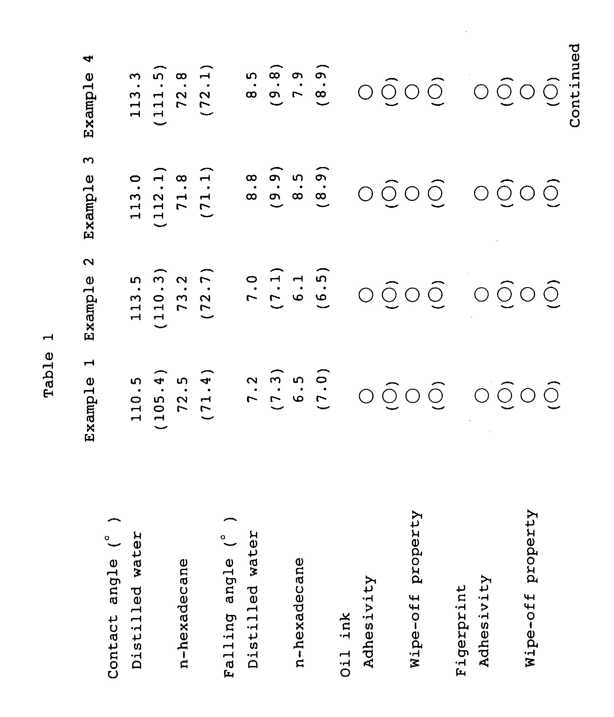

Claims (36)
- An anti-smudge agent characterized by containing an organosilicon compound represented by the following general formula (1):
- The anti-smudge agent according to claim 1, characterized in that said R2 in said general formula (1) is alkoxy group having 1 to 10 carbon atoms.
- An anti-smudge agent characterized by containing an organosilicon compound represented by the following general formula (3):wherein Rf2 is a linear or branched perfluoroalkyl group having 1 to 16 carbon atoms; R3 is an alkyl group having 1 to 10 carbon atoms; X is a halogen atom; n2 is an integer of 1 to 50; m2 is an integer of 0 to 3; 12 is an integer of 0 to 3; and s2 is an integer of 1 to 6; a is an integer of 0 to 3; b is an integer of 0 to 3; c is 0 or 1; d is 0 or 1; with a proviso that these m2, 12, a, b, c and d meet the conditions of 6≧m2+12>0, a+b=3, and c+d=1.

- The anti-smudge agent according to claim 3, characterized in that said organosilicon compound is formed of a first organosilicon compound represented by said general formula (3) and a second organosilicon compound represented by said general formula (3), and said first organosilicon compound and said second organosilicon compound are different from each other in the components "a", "b", "c" and "d" in said general formula (3).
- A method of forming an anti-smudge layer characterized by comprising a step of depositing the anti-smudge agent of claim 1 on a treating substrate by means of a wet coating method.
- The method of forming an anti-smudge layer according to claim 5, characterized in that further comprising a step of subjecting said anti-smudge layer that has been formed on the treating substrate by making use of said anti-smudge agent to heating, humidification, light irradiation, or electron beam irradiation.
- A method of forming an anti-smudge layer characterized by comprising a step of depositing the anti-smudge agent of claim 3 on a treating substrate by means of a wet coating method.
- The method of forming an anti-smudge layer according to claim 7, characterized in that further comprising a step of subjecting said anti-smudge layer that has been formed on the treating substrate by making use of said anti-smudge agent to heating, humidification, light irradiation, or electron beam irradiation.
- A method of forming an anti-smudge layer characterized by comprising a step of depositing the anti-smudge agent of claim 1 on a treating substrate by means of a dry coating method.
- The method of forming an anti-smudge layer according to claim 9, characterized in that further comprising a step of subjecting said anti-smudge layer that has been formed on the treating substrate by making use of said anti-smudge agent to heating, humidification, light irradiation, or electron beam irradiation.
- A method of forming an anti-smudge layer characterized by comprising a step of depositing the anti-smudge agent of claim 3 on a treating substrate by means of a dry coating method.
- The method of forming an anti-smudge layer according to claim 11, characterized in that further comprising a step of subjecting said anti-smudge layer that has been formed on the treating substrate by making use of said anti-smudge agent to heating, humidification, light irradiation, or electron beam irradiation.
- A method of forming an anti-smudge layer characterized by comprising the steps of;impregnating a porous molded body with the anti-smudge agent of claim 1; andheating said porous molded body impregnated with said anti-smudge agent in vacuum thereby to evaporate said anti-smudge agent and to form an anti-smudge layer on a treating substrate.
- The method of forming an anti-smudge layer according to claim 13, characterized in that further comprising a step of subjecting said anti-smudge layer that has been formed on the treating substrate by making use of said anti-smudge agent to heating, humidification, light irradiation, or electron beam irradiation.
- The method of forming an anti-smudge layer according to claim 13, characterized in that said porous molded body is constituted by at least one kind of materials selected from the group consisting of SiO2, TiO2, ZrO2, MgO, Al2O3, CaSO4, Cu, Fe, Al, stainless steel and carbon.
- The method of forming an anti-smudge layer according to claim 13, characterized in that the heating method for evaporating said anti-smudge agent impregnated in said porous molded body is at least one method selected from a resistance heating method, an electron beam heating method, ion beam heating method, high frequency heating method and a light heating method.
- A method of forming an anti-smudge layer characterized by comprising the steps of;impregnating a porous molded body with the anti-smudge agent of claim 3; andheating said porous molded body impregnated with said anti-smudge agent in vacuum thereby to evaporate said anti-smudge agent and to form an anti-smudge layer on a treating substrate.
- The method of forming an anti-smudge layer according to claim 17, characterized in that further comprising a step of subjecting said anti-smudge layer that has been formed on the treating substrate by making use of said anti-smudge agent to heating, humidification, light irradiation, or electron beam irradiation.
- The method of forming an anti-smudge layer according to claim 17, characterized in that said porous molded body is constituted by at least one kind of materials selected from the group consisting of SiO2, TiO2, ZrO2, MgO, Al2O3, CaSO4, Cu, Fe, Al, stainless steel and carbon.
- The method of forming an anti-smudge layer according to claim 17, characterized in that the heating method for evaporating said anti-smudge agent impregnated in said porous molded body is at least one method selected from a resistance heating method, an electron beam heating method, ion beam heating method, high frequency heating method and a light heating method.
- A reflection preventive optical member comprising a transparent substrate; a reflection preventive film formed on at least one surface of said transparent substrate; and an anti-smudge layer formed on an outermost surface; characterized in that said anti-smudge layer contains the anti-smudge agent of claim 1.
- The reflection preventive optical member according to claim 21, characterized in that said transparent substrate is an organic substrate formed of a transparent substrate or an inorganic substrate formed of a glass substrate.
- A reflection preventive optical member comprising a transparent substrate; a reflection preventive film formed on at least one surface of said transparent substrate; and an anti-smudge layer formed on an outermost surface; characterized in that said anti-smudge layer contains the anti-smudge agent of claim 3.
- The reflection preventive optical member according to claim 23, characterized in that said transparent substrate is an organic substrate formed of a transparent substrate or an inorganic substrate formed of a glass substrate.
- An optical functional member characterized by comprising the reflection preventive optical member of claim 21; and a functional optical member adhered to said reflection preventive optical member.
- The optical functional member according to claim 25, characterized in that said functional optical member is a polarizing plate.
- An optical functional member characterized by comprising the reflection preventive optical member of claim 23; and a functional optical member adhered to said reflection preventive optical member.
- The optical functional member according to claim 27, characterized in that said functional optical member is a polarizing plate.
- A display device comprising a display screen having front face, on the surface of which a coat member is adhered via an adhesive, characterized in that said coat member is the optical functional member of claim 25.
- A display device comprising a display screen having front face, on the surface of which a coat member is adhered via an adhesive, characterized in that said coat member is the optical functional member of claim 26.
- A display device comprising a display screen having front face, on the surface of which a coat member is adhered via an adhesive, characterized in that said coat member is the optical functional member of claim 27.
- A display device comprising a display screen having front face, on the surface of which a coat member is adhered via an adhesive, characterized in that said coat member is the optical functional member of claim 28.
- The display device according to claim 29, characterized in that said display is a liquid crystal display, a CRT display, a projection television, a plasma display, or an EL display.
- The display device according to claim 30, characterized in that said display is a liquid crystal display, a CRT display, a projection television, a plasma display, or an EL display.
- The display device according to claim 31, characterized in that said display is a liquid crystal display, a CRT display, a projection television, a plasma display, or an EL display.
- The display device according to claim 32, characterized in that said display is a liquid crystal display, a CRT display, a projection television, a plasma display, or an EL display.
Applications Claiming Priority (4)
| Application Number | Priority Date | Filing Date | Title |
|---|---|---|---|
| JP3432898 | 1998-01-31 | ||
| JP3432898 | 1998-01-31 | ||
| JP25408998 | 1998-09-08 | ||
| JP25408998 | 1998-09-08 |
Publications (3)
| Publication Number | Publication Date |
|---|---|
| EP0933377A2 true EP0933377A2 (en) | 1999-08-04 |
| EP0933377A3 EP0933377A3 (en) | 2000-12-27 |
| EP0933377B1 EP0933377B1 (en) | 2004-11-24 |
Family
ID=26373111
Family Applications (1)
| Application Number | Title | Priority Date | Filing Date |
|---|---|---|---|
| EP99101960A Expired - Lifetime EP0933377B1 (en) | 1998-01-31 | 1999-01-29 | Anti-smudge agent, method of forming an anti-smudge layer, anti-reflection optical member and display device |
Country Status (9)
| Country | Link |
|---|---|
| EP (1) | EP0933377B1 (en) |
| JP (1) | JP4733798B2 (en) |
| KR (1) | KR100664904B1 (en) |
| AT (1) | ATE283274T1 (en) |
| CA (1) | CA2260420A1 (en) |
| DE (1) | DE69922064T2 (en) |
| DK (1) | DK0933377T3 (en) |
| ES (1) | ES2232981T3 (en) |
| TW (1) | TW483930B (en) |
Cited By (51)
| Publication number | Priority date | Publication date | Assignee | Title |
|---|---|---|---|---|
| WO2000034408A1 (en) * | 1998-12-10 | 2000-06-15 | Toray Industries, Inc. | Optical article, method for preparing optical article and organic silicon compound |
| WO2002025687A1 (en) * | 2000-09-21 | 2002-03-28 | Koninklijke Philips Electronics N.V. | Reflective polarizer for a display device |
| US6482911B1 (en) | 2001-05-08 | 2002-11-19 | 3M Innovative Properties Company | Fluoroalkyl polymers containing a cationogenic segment |
| FR2824821A1 (en) | 2001-05-17 | 2002-11-22 | Essilor Int | Preparation of an optical glass with a hydrophobic and/or oil-repellent coating for edge grinding by providing a temporary protective layer conferring an improved surface energy for retaining purposes |
| WO2003057641A1 (en) | 2002-01-14 | 2003-07-17 | Essilor International Compagnie Generale D'optique | Process for treating an ophthalmic lens |
| US6613860B1 (en) | 2000-10-12 | 2003-09-02 | 3M Innovative Properties Company | Compositions comprising fluorinated polyether silanes for rendering substrates oil and water repellent |
| US6649272B2 (en) | 2001-11-08 | 2003-11-18 | 3M Innovative Properties Company | Coating composition comprising fluorochemical polyether silane polycondensate and use thereof |
| EP1380858A1 (en) * | 2002-07-03 | 2004-01-14 | Cosmos Vacuum Technology Corporation | Method for manufacturing an anti-reflective coating on a substrate for the production of a polarizer |
| US6716534B2 (en) | 2001-11-08 | 2004-04-06 | 3M Innovative Properties Company | Coating composition comprising a fluorochemical polyether silane partial condensate and use thereof |
| US6977307B2 (en) | 2001-01-19 | 2005-12-20 | 3M Innovative Properties Company | Water soluble or water dispersible fluorochemical silanes for rendering substrates oil and water repellent |
| DE102004044441B3 (en) * | 2004-09-14 | 2006-06-01 | Rodenstock Gmbh | Improvement of the grinding and stamping behavior of spectacle lenses with hydrophobic coating |
| US7166329B2 (en) | 2001-01-19 | 2007-01-23 | 3M Innovative Properties Company | Method of rendering substrates oil and water repellent with a fluorochemical oligomeric silane |
| US7217440B2 (en) | 2003-06-13 | 2007-05-15 | Essilor International Compagnie Generale D'optique | Process for replacing an initial outermost coating layer of a coated optical lens with a different coating layer or by depositing thereon a different coating layer |
| WO2008073689A1 (en) * | 2006-12-15 | 2008-06-19 | 3M Innovative Properties Company | Fluorochemical urethane compounds having pendent silyl groups used for surface treatment |
| US7470741B2 (en) | 2002-06-03 | 2008-12-30 | 3M Innovative Properties Company | Fluorochemical composition and method of treatment of a substrate therewith to render substrate oil- and/or water repellent |
| US7488509B2 (en) | 2003-06-13 | 2009-02-10 | Essilor International Compagnie Generale D'optique | Method for treating a lens apt to trimming |
| US7678464B2 (en) | 2004-10-22 | 2010-03-16 | Essilor International Compagnie Generale D'optique | Substrate with anti-soiling coating |
| WO2010061145A1 (en) | 2008-11-27 | 2010-06-03 | Essilor International (Compagnie Generale D'optique) | Method for manufacturing an optical article with anti-glare properties |
| WO2010147738A1 (en) | 2009-05-29 | 2010-12-23 | Corning Incorporated | Super non-wetting, anti-fingerprint coatings for glass |
| US7990616B2 (en) * | 2007-11-16 | 2011-08-02 | Epson Toyocom Corporation | IR-UV cut multilayer filter with dust repellent property |
| WO2011095626A2 (en) | 2010-02-08 | 2011-08-11 | Essilor International (Compagnie Generale D'optique) | Optical article comprising an anti-reflecting coating having anti-fogging properties |
| US8082756B2 (en) | 2005-12-19 | 2011-12-27 | Essilor International Compagnie Generale D'optique | Method for improving the edging of an optical article by providing a temporary layer of an organic material |
| US8163354B2 (en) | 2006-05-29 | 2012-04-24 | Essilor International Compagnie Generale D'optique | Process for obtaining a hard coated article having anti-fouling properties |
| WO2012076714A1 (en) | 2010-12-10 | 2012-06-14 | Essilor International (Compagnie Generale D'optique) | Optical article comprising an antireflective coating with a low reflection both in the ultraviolet region and in the visible region |
| US8211544B2 (en) | 2005-04-01 | 2012-07-03 | Daikin Industries, Ltd. | Surface modifier |
| WO2012108866A1 (en) | 2011-02-10 | 2012-08-16 | Essilor International (Compagnie Generale D'optique) | Process of drilling organic glasses using a thermoplastic film protecting against cracking and crazing |
| EP2512696A2 (en) * | 2009-12-17 | 2012-10-24 | 3M Innovative Properties Company | Sulfonate-functional coatings and methods |
| WO2012173596A1 (en) | 2011-06-13 | 2012-12-20 | Essilor Internation (Compagnie General D'optique) | Method for obtaining optical articles having superior abrasion resistant properties, and coated articles prepared according to such method |
| US8679637B2 (en) | 2003-09-26 | 2014-03-25 | Essilor International Compagnie Generale D'optique | Electrostatic film coated ophthalmic lens and method for edging same |
| WO2014086501A1 (en) | 2012-12-04 | 2014-06-12 | Essilor International (Compagnie Generale D'optique) | Method for coating an optical article with a topcoat using vacuum air plasma treatment |
| US8817376B2 (en) | 2011-11-30 | 2014-08-26 | Corning Incorporated | Optical coating method, apparatus and product |
| WO2015000534A1 (en) | 2013-07-05 | 2015-01-08 | Essilor International (Compagnie Generale D'optique) | Optical article comprising an antireflective coating with a very low reflection in the visible region |
| US8945684B2 (en) | 2005-11-04 | 2015-02-03 | Essilor International (Compagnie Generale D'optique) | Process for coating an article with an anti-fouling surface coating by vacuum evaporation |
| EP2851713A1 (en) | 2013-09-20 | 2015-03-25 | ESSILOR INTERNATIONAL (Compagnie Générale d'Optique) | Optical article with gradient photochromism |
| DE102013020551A1 (en) | 2013-12-12 | 2015-06-18 | Merck Patent Gmbh | Emulsions of perfluoropolyethers |
| US9134461B2 (en) | 2006-03-27 | 2015-09-15 | Essilor International (Compagnie Generale D'optique) | Edging process of lens using transparent coating layer for protecting lens |
| WO2015177586A1 (en) | 2014-05-20 | 2015-11-26 | Essilor International (Compagnie Generale D'optique) | Optical lens coated with a patterned removable film and method for edging such a lens |
| WO2016034914A1 (en) | 2014-09-04 | 2016-03-10 | Essilor International (Compagnie Generale D'optique) | Optical lens comprising a protective removable film |
| WO2016102857A1 (en) | 2014-12-24 | 2016-06-30 | Essilor International (Compagnie Générale d'Optique) | Optical article comprising an interference coating with high reflectivity in the ultraviolet region |
| EP3045940A1 (en) | 2014-12-31 | 2016-07-20 | Essilor International (Compagnie Generale D'optique) | Ophthalmic lens comprising an anti-reflective coating designed for scotopic conditions |
| EP3124646A1 (en) | 2015-07-30 | 2017-02-01 | ESSILOR INTERNATIONAL (Compagnie Générale d'Optique) | Machine for coating an optical article and assembly and method including or carrying out this machine |
| EP3124222A1 (en) | 2015-07-30 | 2017-02-01 | ESSILOR INTERNATIONAL (Compagnie Générale d'Optique) | System for coating an optical article with a predetermined coating composition, coating device for such a system and method for using the system |
| EP3185050A1 (en) | 2015-12-23 | 2017-06-28 | Essilor International (Compagnie Générale D'Optique) | Optical article comprising a multilayered interferential coating obtained from an organic precursor or a mixture of organic precursors |
| EP3190436A1 (en) | 2009-03-27 | 2017-07-12 | Essilor International (Compagnie Generale D'optique) | Optical article coated with an antireflection or reflective coating comprising an electrically conductive film based on tin oxide, and production method |
| WO2018033687A1 (en) | 2016-08-19 | 2018-02-22 | Essilor International | Ophthalmic lens comprising a reflective anti-abrasion multilayer coating and process for manufacturing said lens |
| US9957609B2 (en) | 2011-11-30 | 2018-05-01 | Corning Incorporated | Process for making of glass articles with optical and easy-to-clean coatings |
| EP3581675A1 (en) | 2018-06-15 | 2019-12-18 | Corporation de L'Ecole Polytechnique de Montreal | Optical article having directional micro- or nanostructured thin film coating, and its process |
| US10830925B2 (en) | 2014-08-05 | 2020-11-10 | Essilor International | Method for reducing or preventing the degradation of an antifouling layer or an optical article |
| US11427503B2 (en) | 2017-06-23 | 2022-08-30 | AGC Inc. | Chemically-strengthened glass |
| CN115403972A (en) * | 2022-09-04 | 2022-11-29 | 合肥乐凯科技产业有限公司 | Light-resistant curtain and preparation method thereof |
| WO2024023177A1 (en) | 2022-07-26 | 2024-02-01 | Essilor International | Method and system for obtaining a customized optical article having at least one predetermined optical property |
Families Citing this family (33)
| Publication number | Priority date | Publication date | Assignee | Title |
|---|---|---|---|---|
| KR100551135B1 (en) * | 1999-03-09 | 2006-02-10 | 주식회사 새 한 | Producing method of the reflection preventive transparent sheet with a excellent antipollution |
| JP2002083989A (en) * | 2000-09-08 | 2002-03-22 | Toppan Printing Co Ltd | Solar cell module |
| KR20020095890A (en) * | 2001-06-18 | 2002-12-28 | 주식회사 엘지이아이 | The Coating Structure of the C-CRT |
| KR100455141B1 (en) * | 2001-12-31 | 2004-11-06 | 엘지전자 주식회사 | Power saving apparatus for lcd of mobile telecommunication terminal equipment |
| WO2004075279A1 (en) | 2003-02-18 | 2004-09-02 | Konica Minolta Holdings, Inc. | Organic thin-film transistor device and method for manufacturing same |
| US20070253051A1 (en) | 2003-09-29 | 2007-11-01 | Kunihiko Ishihara | Optical Device |
| JP4961738B2 (en) * | 2005-12-21 | 2012-06-27 | 凸版印刷株式会社 | Conductive laminate and display |
| US20100028682A1 (en) * | 2006-09-29 | 2010-02-04 | Seiji Shinohara | Optical functional film |
| WO2010038648A1 (en) * | 2008-10-01 | 2010-04-08 | 株式会社ティーアンドケー | Coating composition, method of antifouling treatment and antifouling substrate |
| JP2013028728A (en) | 2011-07-28 | 2013-02-07 | Nitto Denko Corp | Method of reusably separating two adhered plates and apparatus used for the method |
| US10077207B2 (en) | 2011-11-30 | 2018-09-18 | Corning Incorporated | Optical coating method, apparatus and product |
| CN104114566B (en) | 2012-02-17 | 2017-05-31 | 旭硝子株式会社 | Fluorine-containing ether compound, fluorine-containing ether composition and coating liquid and base material and its manufacture method with surface-treated layer |
| TWI582181B (en) | 2012-02-17 | 2017-05-11 | Asahi Glass Co Ltd | A fluorine-containing ether compound, a fluorine-containing ether composition and a coating liquid, and a substrate having a surface treatment layer and a method for producing the same (1) |
| JP2014194530A (en) * | 2013-02-28 | 2014-10-09 | Asahi Glass Co Ltd | Optical element |
| KR101524271B1 (en) * | 2013-03-11 | 2015-05-29 | (주) 개마텍 | A composition of anti-fingerprint coating layer with a plurality of thin films and method of manufacturing the same. |
| US10150889B2 (en) | 2013-09-16 | 2018-12-11 | Honeywell International Inc. | Poly fluorine-containing siloxane coatings |
| CN105209568B (en) * | 2014-04-23 | 2018-04-13 | 凯玛科技株式会社 | Composition of anti-fingerprint layer formed by multiple films and preparation method thereof |
| KR20170117811A (en) | 2016-04-14 | 2017-10-24 | 현대자동차주식회사 | Anti-Pollution Surface Coating Materials |
| EP3643495B1 (en) | 2017-06-21 | 2023-11-01 | AGC Inc. | Article having water- and oil-repellent layer formed thereon, and method for manufacturing same |
| CN111246997A (en) * | 2017-10-19 | 2020-06-05 | Agc株式会社 | Transparent substrate laminate and method for producing same |
| JP7124866B2 (en) | 2018-05-09 | 2022-08-24 | コニカミノルタ株式会社 | Inkjet head and image forming method |
| KR20210089638A (en) | 2018-11-13 | 2021-07-16 | 에이지씨 가부시키가이샤 | Method for manufacturing a substrate for forming a water and oil repellent layer, a vapor deposition material, and a substrate for forming a water and oil repellent layer |
| EP3904305A4 (en) | 2018-12-26 | 2022-10-05 | Agc Inc. | Water-and-oil repellent layer-attached substrate, and method for manufacturing same |
| JP7188456B2 (en) | 2019-01-11 | 2022-12-13 | コニカミノルタ株式会社 | Inkjet head, inkjet head manufacturing method, and inkjet recording method |
| EP3922626A4 (en) | 2019-02-08 | 2022-11-23 | Agc Inc. | Fluorine-containing ether compound, fluorine-containing ether composition, coating liquid, article, method for producing article, and method for producing fluorine-containing compound |
| CN114096489B (en) | 2019-07-17 | 2024-02-20 | Agc株式会社 | Glass, chemically strengthened glass and protective glass |
| WO2021019693A1 (en) | 2019-07-30 | 2021-02-04 | コニカミノルタ株式会社 | Nozzle plate, nozzle plate manufacturing method, and inkjet head |
| EP4032933A4 (en) | 2019-09-20 | 2024-03-20 | Agc Inc | Fluorine-containing ether compound, surface treatment agent, fluorine-containing ether composition, coating liquid, article, and compound |
| JP7351512B2 (en) | 2019-10-01 | 2023-09-27 | 日東化成株式会社 | Antifouling paint composition |
| CN114867730A (en) * | 2019-12-26 | 2022-08-05 | Agc株式会社 | Fluorine-containing ether compound, surface treatment agent, fluorine-containing ether composition, coating liquid, article, and method for producing article |
| CN115916528B (en) * | 2020-07-13 | 2024-03-12 | 日东电工株式会社 | Optical film with antifouling layer |
| JPWO2022044245A1 (en) | 2020-08-28 | 2022-03-03 | ||
| JP7385058B2 (en) | 2021-06-18 | 2023-11-21 | キヤノンオプトロン株式会社 | Surface layer, optical member, eyeglasses, and surface layer forming material |
Citations (4)
| Publication number | Priority date | Publication date | Assignee | Title |
|---|---|---|---|---|
| US4687707A (en) * | 1984-06-26 | 1987-08-18 | Asahi Glass Company Ltd. | Low reflectance transparent material having antisoiling properties |
| US4944962A (en) * | 1987-10-24 | 1990-07-31 | Ito Optical Industrial Co., Ltd. | Method for dirtproofing treatment for plastic lens |
| US5461173A (en) * | 1993-12-27 | 1995-10-24 | Shin-Etsu Chemical Co., Ltd. | Fluorine-containing organosilicon compound and its manufacture |
| EP0797111A2 (en) * | 1996-03-21 | 1997-09-24 | Sony Corporation | Composition for forming an antifouling film, optical component and display device |
Family Cites Families (14)
| Publication number | Priority date | Publication date | Assignee | Title |
|---|---|---|---|---|
| JPS58142958A (en) * | 1982-02-19 | 1983-08-25 | Asahi Glass Co Ltd | Water and oil repellent for glass surface |
| JPS61241143A (en) * | 1985-04-19 | 1986-10-27 | 旭硝子株式会社 | Low reflective plastic having antifouling property |
| JPS61215235A (en) * | 1985-03-19 | 1986-09-25 | Asahi Glass Co Ltd | Glass of low reflectance having stain resistance |
| JPS6110043A (en) * | 1984-06-26 | 1986-01-17 | Asahi Glass Co Ltd | Glass of low reflectance having anti-staining property |
| JPS63250389A (en) * | 1987-04-03 | 1988-10-18 | Shin Etsu Chem Co Ltd | Fluorine-containing organosilicon compound and production thereof |
| JPH0726062B2 (en) * | 1988-08-22 | 1995-03-22 | 株式会社トクヤマ | Surface treatment agent for inorganic coated film |
| JP2991513B2 (en) * | 1990-06-08 | 1999-12-20 | 旭硝子株式会社 | Sealant or paint containing antifouling agent |
| JP2877616B2 (en) * | 1992-05-29 | 1999-03-31 | 信越化学工業株式会社 | Hydrophilic oil repellent treatment agent |
| JP3574158B2 (en) * | 1993-05-14 | 2004-10-06 | セイコーエプソン株式会社 | Liquid crystal display |
| JP3629755B2 (en) * | 1995-04-27 | 2005-03-16 | 旭硝子株式会社 | Surface-treated substrate and method for producing the same |
| ATE443117T1 (en) * | 1996-05-31 | 2009-10-15 | Toto Ltd | ANTIFOULING ELEMENTS AND ANTIFOULING COATING COMPOSITION |
| JP3503365B2 (en) * | 1996-10-25 | 2004-03-02 | 旭硝子株式会社 | Surface treated substrate |
| JPH10193489A (en) * | 1996-11-14 | 1998-07-28 | Canon Inc | Thin film forming material and forming method for thin film |
| KR19980072164A (en) * | 1998-07-28 | 1998-10-26 | 이영만 | Securities information terminal device using two-way wireless data communication |
-
1999
- 1999-01-27 JP JP01860199A patent/JP4733798B2/en not_active Expired - Lifetime
- 1999-01-28 CA CA002260420A patent/CA2260420A1/en not_active Abandoned
- 1999-01-29 ES ES99101960T patent/ES2232981T3/en not_active Expired - Lifetime
- 1999-01-29 DE DE69922064T patent/DE69922064T2/en not_active Expired - Fee Related
- 1999-01-29 AT AT99101960T patent/ATE283274T1/en not_active IP Right Cessation
- 1999-01-29 EP EP99101960A patent/EP0933377B1/en not_active Expired - Lifetime
- 1999-01-29 DK DK99101960T patent/DK0933377T3/en active
- 1999-01-29 KR KR1019990002904A patent/KR100664904B1/en not_active IP Right Cessation
- 1999-01-29 TW TW088101405A patent/TW483930B/en not_active IP Right Cessation
Patent Citations (4)
| Publication number | Priority date | Publication date | Assignee | Title |
|---|---|---|---|---|
| US4687707A (en) * | 1984-06-26 | 1987-08-18 | Asahi Glass Company Ltd. | Low reflectance transparent material having antisoiling properties |
| US4944962A (en) * | 1987-10-24 | 1990-07-31 | Ito Optical Industrial Co., Ltd. | Method for dirtproofing treatment for plastic lens |
| US5461173A (en) * | 1993-12-27 | 1995-10-24 | Shin-Etsu Chemical Co., Ltd. | Fluorine-containing organosilicon compound and its manufacture |
| EP0797111A2 (en) * | 1996-03-21 | 1997-09-24 | Sony Corporation | Composition for forming an antifouling film, optical component and display device |
Non-Patent Citations (1)
| Title |
|---|
| DATABASE WPI Section Ch, Week 199237 Derwent Publications Ltd., London, GB; Class A26, AN 1992-305510 XP002151919 -& JP 04 213384 A (ASAHI GLASS CO LTD), 4 August 1992 (1992-08-04) * |
Cited By (84)
| Publication number | Priority date | Publication date | Assignee | Title |
|---|---|---|---|---|
| WO2000034408A1 (en) * | 1998-12-10 | 2000-06-15 | Toray Industries, Inc. | Optical article, method for preparing optical article and organic silicon compound |
| EP1055718A1 (en) * | 1998-12-10 | 2000-11-29 | Toray Industries, Inc. | Optical article, method for preparing optical article and organic silicon compound |
| EP1055718A4 (en) * | 1998-12-10 | 2005-01-05 | Toray Industries | Optical article, method for preparing optical article and organic silicon compound |
| WO2002025687A1 (en) * | 2000-09-21 | 2002-03-28 | Koninklijke Philips Electronics N.V. | Reflective polarizer for a display device |
| US6613860B1 (en) | 2000-10-12 | 2003-09-02 | 3M Innovative Properties Company | Compositions comprising fluorinated polyether silanes for rendering substrates oil and water repellent |
| US7166329B2 (en) | 2001-01-19 | 2007-01-23 | 3M Innovative Properties Company | Method of rendering substrates oil and water repellent with a fluorochemical oligomeric silane |
| US6977307B2 (en) | 2001-01-19 | 2005-12-20 | 3M Innovative Properties Company | Water soluble or water dispersible fluorochemical silanes for rendering substrates oil and water repellent |
| US6482911B1 (en) | 2001-05-08 | 2002-11-19 | 3M Innovative Properties Company | Fluoroalkyl polymers containing a cationogenic segment |
| FR2824821A1 (en) | 2001-05-17 | 2002-11-22 | Essilor Int | Preparation of an optical glass with a hydrophobic and/or oil-repellent coating for edge grinding by providing a temporary protective layer conferring an improved surface energy for retaining purposes |
| US9278885B2 (en) | 2001-05-17 | 2016-03-08 | Essilor International Compagnie Generale D'optique | Method for preparing a glass convenient for trimming, a glass thus obtained, and method for trimming such a glass |
| US8962141B2 (en) | 2001-05-17 | 2015-02-24 | Essilor International Compagnie Generale D'optique | Method for preparing a glass convenient for trimming, a glass thus obtained, and method for trimming such a glass |
| US8252368B2 (en) | 2001-05-17 | 2012-08-28 | Essilor International Compagnie Generale D 'optique | Method for preparing a glass convenient for trimming, a glass thus obtained, and method for trimming such a glass |
| US6649272B2 (en) | 2001-11-08 | 2003-11-18 | 3M Innovative Properties Company | Coating composition comprising fluorochemical polyether silane polycondensate and use thereof |
| US6716534B2 (en) | 2001-11-08 | 2004-04-06 | 3M Innovative Properties Company | Coating composition comprising a fluorochemical polyether silane partial condensate and use thereof |
| US7094471B2 (en) | 2001-11-08 | 2006-08-22 | 3M Innovative Properties Company | Coating composition comprising a fluorochemical polyether silane partial condensate and use thereof |
| US7097910B2 (en) | 2001-11-08 | 2006-08-29 | 3M Innovative Properties Company | Coating composition comprising fluorochemical polyether silane polycondensate and use thereof |
| US7629053B2 (en) | 2002-01-14 | 2009-12-08 | Essilor International Compagnie Generale D'optique | Process for treating an ophthalmic lens |
| WO2003057641A1 (en) | 2002-01-14 | 2003-07-17 | Essilor International Compagnie Generale D'optique | Process for treating an ophthalmic lens |
| FR2834712A1 (en) | 2002-01-14 | 2003-07-18 | Essilor Int | PROCESS FOR TREATING OPHTHALMIC GLASS |
| US7470741B2 (en) | 2002-06-03 | 2008-12-30 | 3M Innovative Properties Company | Fluorochemical composition and method of treatment of a substrate therewith to render substrate oil- and/or water repellent |
| EP1380858A1 (en) * | 2002-07-03 | 2004-01-14 | Cosmos Vacuum Technology Corporation | Method for manufacturing an anti-reflective coating on a substrate for the production of a polarizer |
| US8309168B2 (en) | 2003-06-13 | 2012-11-13 | Essilor International Compagnie Generale D'optique | Method for treating a lens apt to trimming and lens apt to trimming |
| EP2088133A2 (en) | 2003-06-13 | 2009-08-12 | Essilor International (Compagnie Générale D'Optique) | Method for obtaining a lens apt to trimming |
| US7488509B2 (en) | 2003-06-13 | 2009-02-10 | Essilor International Compagnie Generale D'optique | Method for treating a lens apt to trimming |
| US7217440B2 (en) | 2003-06-13 | 2007-05-15 | Essilor International Compagnie Generale D'optique | Process for replacing an initial outermost coating layer of a coated optical lens with a different coating layer or by depositing thereon a different coating layer |
| US8679637B2 (en) | 2003-09-26 | 2014-03-25 | Essilor International Compagnie Generale D'optique | Electrostatic film coated ophthalmic lens and method for edging same |
| US7635523B2 (en) | 2004-09-14 | 2009-12-22 | Rodenstock Gmbh | Grinding and stamping behavior of ophthalmic glasses with hydrophobic coating |
| DE102004044441B3 (en) * | 2004-09-14 | 2006-06-01 | Rodenstock Gmbh | Improvement of the grinding and stamping behavior of spectacle lenses with hydrophobic coating |
| US7678464B2 (en) | 2004-10-22 | 2010-03-16 | Essilor International Compagnie Generale D'optique | Substrate with anti-soiling coating |
| US8211544B2 (en) | 2005-04-01 | 2012-07-03 | Daikin Industries, Ltd. | Surface modifier |
| US8945684B2 (en) | 2005-11-04 | 2015-02-03 | Essilor International (Compagnie Generale D'optique) | Process for coating an article with an anti-fouling surface coating by vacuum evaporation |
| US8082756B2 (en) | 2005-12-19 | 2011-12-27 | Essilor International Compagnie Generale D'optique | Method for improving the edging of an optical article by providing a temporary layer of an organic material |
| US11061171B2 (en) | 2005-12-19 | 2021-07-13 | Essilor International | Method for improving the edging of an optical article by providing a temporary layer of an organic matter |
| US9134461B2 (en) | 2006-03-27 | 2015-09-15 | Essilor International (Compagnie Generale D'optique) | Edging process of lens using transparent coating layer for protecting lens |
| US8163354B2 (en) | 2006-05-29 | 2012-04-24 | Essilor International Compagnie Generale D'optique | Process for obtaining a hard coated article having anti-fouling properties |
| US8002886B2 (en) | 2006-12-15 | 2011-08-23 | 3M Innovative Properties Company | Fluorochemical urethane compounds having pendent silyl groups used for surface treatment |
| WO2008073689A1 (en) * | 2006-12-15 | 2008-06-19 | 3M Innovative Properties Company | Fluorochemical urethane compounds having pendent silyl groups used for surface treatment |
| US7990616B2 (en) * | 2007-11-16 | 2011-08-02 | Epson Toyocom Corporation | IR-UV cut multilayer filter with dust repellent property |
| WO2010061145A1 (en) | 2008-11-27 | 2010-06-03 | Essilor International (Compagnie Generale D'optique) | Method for manufacturing an optical article with anti-glare properties |
| EP3190436A1 (en) | 2009-03-27 | 2017-07-12 | Essilor International (Compagnie Generale D'optique) | Optical article coated with an antireflection or reflective coating comprising an electrically conductive film based on tin oxide, and production method |
| WO2010147738A1 (en) | 2009-05-29 | 2010-12-23 | Corning Incorporated | Super non-wetting, anti-fingerprint coatings for glass |
| US10889725B2 (en) | 2009-12-17 | 2021-01-12 | 3M Innovative Properties Company | Sulfonate-functional coatings and methods |
| EP2512696A2 (en) * | 2009-12-17 | 2012-10-24 | 3M Innovative Properties Company | Sulfonate-functional coatings and methods |
| US10160868B2 (en) | 2009-12-17 | 2018-12-25 | 3M Innovative Properties Company | Sulfonate-functional coatings and methods |
| US9340683B2 (en) | 2009-12-17 | 2016-05-17 | 3M Innovative Properties Company | Sulfonate-functional coatings and methods |
| EP2512696B1 (en) * | 2009-12-17 | 2015-07-29 | 3M Innovative Properties Company | Sulfonate-functional coatings and methods |
| WO2011095626A2 (en) | 2010-02-08 | 2011-08-11 | Essilor International (Compagnie Generale D'optique) | Optical article comprising an anti-reflecting coating having anti-fogging properties |
| DE202011110944U1 (en) | 2010-12-10 | 2017-08-09 | Essilor International (Compagnie Generale D'optique) | An optical article having a low reflection antireflection coating in both the ultraviolet and visible regions |
| DE202011110945U1 (en) | 2010-12-10 | 2017-08-09 | Essilor International (Compagnie Generale D'optique) | An optical article having a low reflection antireflection coating in both the ultraviolet and visible regions |
| EP3964873A1 (en) | 2010-12-10 | 2022-03-09 | Essilor International | Optical article comprising an antireflective coating with a low reflection both in the ultraviolet region and in the visible region |
| WO2012076714A1 (en) | 2010-12-10 | 2012-06-14 | Essilor International (Compagnie Generale D'optique) | Optical article comprising an antireflective coating with a low reflection both in the ultraviolet region and in the visible region |
| DE202011110943U1 (en) | 2010-12-10 | 2017-08-09 | Essilor International (Compagnie Generale D'optique) | An optical article having a low reflection antireflection coating in both the ultraviolet and visible regions |
| EP2685293A2 (en) | 2010-12-10 | 2014-01-15 | ESSILOR INTERNATIONAL (Compagnie Générale d'Optique) | Optical article comprising an antireflective coating with a low reflection both in the ultraviolet region and in the visible region |
| WO2012108866A1 (en) | 2011-02-10 | 2012-08-16 | Essilor International (Compagnie Generale D'optique) | Process of drilling organic glasses using a thermoplastic film protecting against cracking and crazing |
| WO2012173596A1 (en) | 2011-06-13 | 2012-12-20 | Essilor Internation (Compagnie General D'optique) | Method for obtaining optical articles having superior abrasion resistant properties, and coated articles prepared according to such method |
| US9957609B2 (en) | 2011-11-30 | 2018-05-01 | Corning Incorporated | Process for making of glass articles with optical and easy-to-clean coatings |
| US9013795B2 (en) | 2011-11-30 | 2015-04-21 | Corning Incorporated | Optical coating method, apparatus and product |
| US8817376B2 (en) | 2011-11-30 | 2014-08-26 | Corning Incorporated | Optical coating method, apparatus and product |
| WO2014086501A1 (en) | 2012-12-04 | 2014-06-12 | Essilor International (Compagnie Generale D'optique) | Method for coating an optical article with a topcoat using vacuum air plasma treatment |
| WO2015000534A1 (en) | 2013-07-05 | 2015-01-08 | Essilor International (Compagnie Generale D'optique) | Optical article comprising an antireflective coating with a very low reflection in the visible region |
| WO2015040184A1 (en) | 2013-09-20 | 2015-03-26 | Essilor International (Compagnie Generale D'optique) | Optical article with gradient photochromism |
| EP2851713A1 (en) | 2013-09-20 | 2015-03-25 | ESSILOR INTERNATIONAL (Compagnie Générale d'Optique) | Optical article with gradient photochromism |
| DE102013020551A1 (en) | 2013-12-12 | 2015-06-18 | Merck Patent Gmbh | Emulsions of perfluoropolyethers |
| WO2015177586A1 (en) | 2014-05-20 | 2015-11-26 | Essilor International (Compagnie Generale D'optique) | Optical lens coated with a patterned removable film and method for edging such a lens |
| US10830925B2 (en) | 2014-08-05 | 2020-11-10 | Essilor International | Method for reducing or preventing the degradation of an antifouling layer or an optical article |
| WO2016034914A1 (en) | 2014-09-04 | 2016-03-10 | Essilor International (Compagnie Generale D'optique) | Optical lens comprising a protective removable film |
| US10562248B2 (en) | 2014-09-04 | 2020-02-18 | Essilor International | Optical lens comprising a protective removable film |
| WO2016102857A1 (en) | 2014-12-24 | 2016-06-30 | Essilor International (Compagnie Générale d'Optique) | Optical article comprising an interference coating with high reflectivity in the ultraviolet region |
| US10288905B2 (en) | 2014-12-24 | 2019-05-14 | Essilor International | Optical article comprising an interference coating with high reflectivity in the ultraviolet region |
| EP3045940A1 (en) | 2014-12-31 | 2016-07-20 | Essilor International (Compagnie Generale D'optique) | Ophthalmic lens comprising an anti-reflective coating designed for scotopic conditions |
| US10605959B2 (en) | 2014-12-31 | 2020-03-31 | Essilor International | Antireflective stack for low luminance conditions |
| US11192315B2 (en) | 2015-07-30 | 2021-12-07 | Essilor International | System for coating an optical article with a predetermined coating composition, coating device for such a system and method for using the system |
| EP3124222A1 (en) | 2015-07-30 | 2017-02-01 | ESSILOR INTERNATIONAL (Compagnie Générale d'Optique) | System for coating an optical article with a predetermined coating composition, coating device for such a system and method for using the system |
| EP3124646A1 (en) | 2015-07-30 | 2017-02-01 | ESSILOR INTERNATIONAL (Compagnie Générale d'Optique) | Machine for coating an optical article and assembly and method including or carrying out this machine |
| EP3185050A1 (en) | 2015-12-23 | 2017-06-28 | Essilor International (Compagnie Générale D'Optique) | Optical article comprising a multilayered interferential coating obtained from an organic precursor or a mixture of organic precursors |
| WO2018033687A1 (en) | 2016-08-19 | 2018-02-22 | Essilor International | Ophthalmic lens comprising a reflective anti-abrasion multilayer coating and process for manufacturing said lens |
| US11427503B2 (en) | 2017-06-23 | 2022-08-30 | AGC Inc. | Chemically-strengthened glass |
| US11661374B2 (en) | 2017-06-23 | 2023-05-30 | AGC Inc. | Chemically-strengthened glass |
| WO2019238836A1 (en) | 2018-06-15 | 2019-12-19 | Corporation De L'ecole Polytechnique De Montreal | Optical article having directional micro- or nanostructured thin film coating, and its process |
| EP3581675A1 (en) | 2018-06-15 | 2019-12-18 | Corporation de L'Ecole Polytechnique de Montreal | Optical article having directional micro- or nanostructured thin film coating, and its process |
| US11867876B2 (en) | 2018-06-15 | 2024-01-09 | Corporation De L'ecole Polytechnique De Montreal | Optical article having directional micro- or nanostructured thin film coating, and its process |
| WO2024023177A1 (en) | 2022-07-26 | 2024-02-01 | Essilor International | Method and system for obtaining a customized optical article having at least one predetermined optical property |
| CN115403972A (en) * | 2022-09-04 | 2022-11-29 | 合肥乐凯科技产业有限公司 | Light-resistant curtain and preparation method thereof |
| CN115403972B (en) * | 2022-09-04 | 2024-03-01 | 合肥乐凯科技产业有限公司 | Light-resistant curtain cloth and preparation method thereof |
Also Published As
| Publication number | Publication date |
|---|---|
| DE69922064D1 (en) | 2004-12-30 |
| JP2000144097A (en) | 2000-05-26 |
| TW483930B (en) | 2002-04-21 |
| KR19990068208A (en) | 1999-08-25 |
| EP0933377A3 (en) | 2000-12-27 |
| ES2232981T3 (en) | 2005-06-01 |
| DK0933377T3 (en) | 2004-12-27 |
| DE69922064T2 (en) | 2006-03-02 |
| CA2260420A1 (en) | 1999-07-31 |
| EP0933377B1 (en) | 2004-11-24 |
| ATE283274T1 (en) | 2004-12-15 |
| JP4733798B2 (en) | 2011-07-27 |
| KR100664904B1 (en) | 2007-01-04 |
Similar Documents
| Publication | Publication Date | Title |
|---|---|---|
| EP0933377B1 (en) | Anti-smudge agent, method of forming an anti-smudge layer, anti-reflection optical member and display device | |
| EP0749021B1 (en) | Antireflection filter | |
| KR100557257B1 (en) | Antisoiling coatings for antireflective surfaces and methods of preparation | |
| US20180099307A1 (en) | Antiglare film-coated substrate, antiglare film forming liquid composition, and method of producing antiglare film-coated substrate | |
| EP1300433B1 (en) | Perfluoropolyether-modified silane, surface treating agent, and antireflection filter | |
| EP2070967B1 (en) | Per-fluoro polyether compound, antifouling coating composition and film containing same | |
| JP4918743B2 (en) | Antireflection film | |
| JP3722418B2 (en) | Antireflection film and optical member using the same | |
| JP6696486B2 (en) | Substrate with antiglare film, liquid composition for forming antiglare film, and method for producing substrate with antiglare film | |
| KR100627747B1 (en) | Optical Article, Method for Preparing Optical Article, and Organic Silicon Compound | |
| CN103551076A (en) | Surface modifier | |
| JP2001048590A (en) | Reflection preventing material | |
| JP2002265866A (en) | Low-refractive index coating material and antireflection film | |
| JP3494195B2 (en) | Anti-reflection filter | |
| JP4478216B2 (en) | DISPLAY DEVICE FILTER, DISPLAY DEVICE, DISPLAY DEVICE FILTER MANUFACTURING METHOD, AND SURFACE MODIFICATION FILM COATING COMPOSITION | |
| JP3787988B2 (en) | Antireflection filter and character image display device using the antireflection filter | |
| JP4174867B2 (en) | Method for forming antifouling layer | |
| JP4420476B2 (en) | Composition for surface modification film, surface modification film, filter for display device, display device and method for producing filter for display device | |
| CN113874334B (en) | Transparent substrate with antifouling layer | |
| JPH10148701A (en) | Antireflection filter, its production, and display device using this antireflection filter | |
| JPH11217558A (en) | Stainproofing agent and formation of stainproofing layer | |
| JP2000009906A (en) | Antireflection optical member, forming method of contamination preventing layer, optical functional member and display device | |
| JP4332931B2 (en) | Optical member and manufacturing method thereof | |
| JP2001004804A (en) | Reflection preventing optical member | |
| JPH11352304A (en) | Antireflection optical member and method for formation of antifouling layer |
Legal Events
| Date | Code | Title | Description |
|---|---|---|---|
| PUAI | Public reference made under article 153(3) epc to a published international application that has entered the european phase |
Free format text: ORIGINAL CODE: 0009012 |
|
| AK | Designated contracting states |
Kind code of ref document: A2 Designated state(s): AT BE CH CY DE DK ES FI FR GB GR IE IT LI LU MC NL PT SE |
|
| AX | Request for extension of the european patent |
Free format text: AL;LT;LV;MK;RO;SI |
|
| PUAL | Search report despatched |
Free format text: ORIGINAL CODE: 0009013 |
|
| RIN1 | Information on inventor provided before grant (corrected) |
Inventor name: HONDA, YOSHITAKA C/O CHEMICAL DIVISION Inventor name: TOMIKAWA, NORITOSHI Inventor name: MIIDA,ATSUSHI Inventor name: OKUBO,TORU Inventor name: WATANABE,NIRO Inventor name: OHATA, KOICHI |
|
| AK | Designated contracting states |
Kind code of ref document: A3 Designated state(s): AT BE CH CY DE DK ES FI FR GB GR IE IT LI LU MC NL PT SE |
|
| AX | Request for extension of the european patent |
Free format text: AL;LT;LV;MK;RO;SI |
|
| RIC1 | Information provided on ipc code assigned before grant |
Free format text: 7C 07F 7/18 A, 7G 02B 1/10 B, 7G 02B 1/11 B |
|
| 17P | Request for examination filed |
Effective date: 20010529 |
|
| AKX | Designation fees paid |
Free format text: AT BE CH CY DE DK ES FI FR GB GR IE IT LI LU MC NL PT SE |
|
| 17Q | First examination report despatched |
Effective date: 20020729 |
|
| GRAP | Despatch of communication of intention to grant a patent |
Free format text: ORIGINAL CODE: EPIDOSNIGR1 |
|
| RAP1 | Party data changed (applicant data changed or rights of an application transferred) |
Owner name: DAIKIN INDUSTRIES, LTD. Owner name: TOPPAN PRINTING CO., LTD. |
|
| GRAS | Grant fee paid |
Free format text: ORIGINAL CODE: EPIDOSNIGR3 |
|
| GRAA | (expected) grant |
Free format text: ORIGINAL CODE: 0009210 |
|
| AK | Designated contracting states |
Kind code of ref document: B1 Designated state(s): AT BE CH CY DE DK ES FI FR GB GR IE IT LI LU MC NL PT SE |
|
| REG | Reference to a national code |
Ref country code: GB Ref legal event code: FG4D |
|
| REG | Reference to a national code |
Ref country code: CH Ref legal event code: EP |
|
| REF | Corresponds to: |
Ref document number: 69922064 Country of ref document: DE Date of ref document: 20041230 Kind code of ref document: P |
|
| REG | Reference to a national code |
Ref country code: IE Ref legal event code: FG4D |
|
| REG | Reference to a national code |
Ref country code: CH Ref legal event code: NV Representative=s name: E. BLUM & CO. PATENTANWAELTE |
|
| PG25 | Lapsed in a contracting state [announced via postgrant information from national office to epo] |
Ref country code: LU Free format text: LAPSE BECAUSE OF NON-PAYMENT OF DUE FEES Effective date: 20050129 Ref country code: IT Free format text: LAPSE BECAUSE OF NON-PAYMENT OF DUE FEES;WARNING: LAPSES OF ITALIAN PATENTS WITH EFFECTIVE DATE BEFORE 2007 MAY HAVE OCCURRED AT ANY TIME BEFORE 2007. THE CORRECT EFFECTIVE DATE MAY BE DIFFERENT FROM THE ONE RECORDED. Effective date: 20050129 Ref country code: CY Free format text: LAPSE BECAUSE OF FAILURE TO SUBMIT A TRANSLATION OF THE DESCRIPTION OR TO PAY THE FEE WITHIN THE PRESCRIBED TIME-LIMIT Effective date: 20050129 |
|
| PG25 | Lapsed in a contracting state [announced via postgrant information from national office to epo] |
Ref country code: MC Free format text: LAPSE BECAUSE OF NON-PAYMENT OF DUE FEES Effective date: 20050131 Ref country code: IE Free format text: LAPSE BECAUSE OF NON-PAYMENT OF DUE FEES Effective date: 20050131 |
|
| PG25 | Lapsed in a contracting state [announced via postgrant information from national office to epo] |
Ref country code: GR Free format text: LAPSE BECAUSE OF FAILURE TO SUBMIT A TRANSLATION OF THE DESCRIPTION OR TO PAY THE FEE WITHIN THE PRESCRIBED TIME-LIMIT Effective date: 20050224 |
|
| REG | Reference to a national code |
Ref country code: SE Ref legal event code: TRGR |
|
| REG | Reference to a national code |
Ref country code: ES Ref legal event code: FG2A Ref document number: 2232981 Country of ref document: ES Kind code of ref document: T3 |
|
| PLBE | No opposition filed within time limit |
Free format text: ORIGINAL CODE: 0009261 |
|
| STAA | Information on the status of an ep patent application or granted ep patent |
Free format text: STATUS: NO OPPOSITION FILED WITHIN TIME LIMIT |
|
| REG | Reference to a national code |
Ref country code: IE Ref legal event code: MM4A |
|
| ET | Fr: translation filed | ||
| 26N | No opposition filed |
Effective date: 20050825 |
|
| REG | Reference to a national code |
Ref country code: CH Ref legal event code: PFA Owner name: TOPPAN PRINTING CO., LTD. Free format text: TOPPAN PRINTING CO., LTD.#5-1, 1-CHOME, TAITO#TAITO-KU, TOKYO (JP) $ DAIKIN INDUSTRIES, LTD.#UMEDA CENTER BLDG., 2-4-12, NAKAZAKI-NISHI, KITA-KU#OSAKA (JP) -TRANSFER TO- TOPPAN PRINTING CO., LTD.#5-1, 1-CHOME, TAITO#TAITO-KU, TOKYO (JP) $ DAIKIN INDUSTRIES, LTD.#UMEDA CENTER BLDG., 2-4-12, NAKAZAKI-NISHI, KITA-KU#OSAKA (JP) |
|
| PG25 | Lapsed in a contracting state [announced via postgrant information from national office to epo] |
Ref country code: PT Free format text: LAPSE BECAUSE OF NON-PAYMENT OF DUE FEES Effective date: 20050424 |
|
| PGFP | Annual fee paid to national office [announced via postgrant information from national office to epo] |
Ref country code: DK Payment date: 20080115 Year of fee payment: 10 Ref country code: CH Payment date: 20080116 Year of fee payment: 10 |
|
| PGFP | Annual fee paid to national office [announced via postgrant information from national office to epo] |
Ref country code: SE Payment date: 20080104 Year of fee payment: 10 Ref country code: FI Payment date: 20080115 Year of fee payment: 10 |
|
| PGFP | Annual fee paid to national office [announced via postgrant information from national office to epo] |
Ref country code: AT Payment date: 20080114 Year of fee payment: 10 |
|
| PGFP | Annual fee paid to national office [announced via postgrant information from national office to epo] |
Ref country code: BE Payment date: 20080407 Year of fee payment: 10 |
|
| PGFP | Annual fee paid to national office [announced via postgrant information from national office to epo] |
Ref country code: ES Payment date: 20090203 Year of fee payment: 11 |
|
| PGFP | Annual fee paid to national office [announced via postgrant information from national office to epo] |
Ref country code: NL Payment date: 20090115 Year of fee payment: 11 Ref country code: DE Payment date: 20090123 Year of fee payment: 11 |
|
| PGFP | Annual fee paid to national office [announced via postgrant information from national office to epo] |
Ref country code: GB Payment date: 20090128 Year of fee payment: 11 |
|
| PGRI | Patent reinstated in contracting state [announced from national office to epo] |
Ref country code: IT Effective date: 20090501 |
|
| PGFP | Annual fee paid to national office [announced via postgrant information from national office to epo] |
Ref country code: IT Payment date: 20090128 Year of fee payment: 11 |
|
| REG | Reference to a national code |
Ref country code: CH Ref legal event code: PL |
|
| EUG | Se: european patent has lapsed | ||
| REG | Reference to a national code |
Ref country code: DK Ref legal event code: EBP |
|
| PG25 | Lapsed in a contracting state [announced via postgrant information from national office to epo] |
Ref country code: LI Free format text: LAPSE BECAUSE OF NON-PAYMENT OF DUE FEES Effective date: 20090131 Ref country code: FI Free format text: LAPSE BECAUSE OF NON-PAYMENT OF DUE FEES Effective date: 20090129 Ref country code: CH Free format text: LAPSE BECAUSE OF NON-PAYMENT OF DUE FEES Effective date: 20090131 Ref country code: AT Free format text: LAPSE BECAUSE OF NON-PAYMENT OF DUE FEES Effective date: 20090129 |
|
| PGFP | Annual fee paid to national office [announced via postgrant information from national office to epo] |
Ref country code: FR Payment date: 20090113 Year of fee payment: 11 |
|
| PG25 | Lapsed in a contracting state [announced via postgrant information from national office to epo] |
Ref country code: BE Free format text: LAPSE BECAUSE OF NON-PAYMENT OF DUE FEES Effective date: 20090131 |
|
| PG25 | Lapsed in a contracting state [announced via postgrant information from national office to epo] |
Ref country code: DK Free format text: LAPSE BECAUSE OF NON-PAYMENT OF DUE FEES Effective date: 20090731 |
|
| REG | Reference to a national code |
Ref country code: NL Ref legal event code: V1 Effective date: 20100801 |
|
| GBPC | Gb: european patent ceased through non-payment of renewal fee |
Effective date: 20100129 |
|
| REG | Reference to a national code |
Ref country code: FR Ref legal event code: ST Effective date: 20100930 |
|
| PG25 | Lapsed in a contracting state [announced via postgrant information from national office to epo] |
Ref country code: NL Free format text: LAPSE BECAUSE OF NON-PAYMENT OF DUE FEES Effective date: 20100801 Ref country code: FR Free format text: LAPSE BECAUSE OF NON-PAYMENT OF DUE FEES Effective date: 20100201 |
|
| PG25 | Lapsed in a contracting state [announced via postgrant information from national office to epo] |
Ref country code: DE Free format text: LAPSE BECAUSE OF NON-PAYMENT OF DUE FEES Effective date: 20100803 |
|
| PG25 | Lapsed in a contracting state [announced via postgrant information from national office to epo] |
Ref country code: GB Free format text: LAPSE BECAUSE OF NON-PAYMENT OF DUE FEES Effective date: 20100129 |
|
| REG | Reference to a national code |
Ref country code: ES Ref legal event code: FD2A Effective date: 20110228 |
|
| PG25 | Lapsed in a contracting state [announced via postgrant information from national office to epo] |
Ref country code: IT Free format text: LAPSE BECAUSE OF NON-PAYMENT OF DUE FEES Effective date: 20100129 |
|
| PG25 | Lapsed in a contracting state [announced via postgrant information from national office to epo] |
Ref country code: SE Free format text: LAPSE BECAUSE OF NON-PAYMENT OF DUE FEES Effective date: 20090130 |
|
| PG25 | Lapsed in a contracting state [announced via postgrant information from national office to epo] |
Ref country code: ES Free format text: LAPSE BECAUSE OF NON-PAYMENT OF DUE FEES Effective date: 20110224 |
|
| PG25 | Lapsed in a contracting state [announced via postgrant information from national office to epo] |
Ref country code: ES Free format text: LAPSE BECAUSE OF NON-PAYMENT OF DUE FEES Effective date: 20100130 |