EP1376671B1 - Compositions for preparing materials with a low dielectric constant - Google Patents
Compositions for preparing materials with a low dielectric constant Download PDFInfo
- Publication number
- EP1376671B1 EP1376671B1 EP03012119A EP03012119A EP1376671B1 EP 1376671 B1 EP1376671 B1 EP 1376671B1 EP 03012119 A EP03012119 A EP 03012119A EP 03012119 A EP03012119 A EP 03012119A EP 1376671 B1 EP1376671 B1 EP 1376671B1
- Authority
- EP
- European Patent Office
- Prior art keywords
- mixture
- solution
- porogen
- butoxysilane
- film
- Prior art date
- Legal status (The legal status is an assumption and is not a legal conclusion. Google has not performed a legal analysis and makes no representation as to the accuracy of the status listed.)
- Expired - Lifetime
Links
- 239000000203 mixture Substances 0.000 title claims abstract description 154
- 239000000463 material Substances 0.000 title abstract description 66
- 239000003361 porogen Substances 0.000 claims abstract description 64
- 238000000034 method Methods 0.000 claims abstract description 51
- 239000013500 performance material Substances 0.000 claims abstract description 9
- IAYPIBMASNFSPL-UHFFFAOYSA-N Ethylene oxide Chemical group C1CO1 IAYPIBMASNFSPL-UHFFFAOYSA-N 0.000 claims abstract description 8
- VYPSYNLAJGMNEJ-UHFFFAOYSA-N Silicium dioxide Chemical compound O=[Si]=O VYPSYNLAJGMNEJ-UHFFFAOYSA-N 0.000 claims description 163
- 239000000377 silicon dioxide Substances 0.000 claims description 81
- 239000003153 chemical reaction reagent Substances 0.000 claims description 61
- 239000002904 solvent Substances 0.000 claims description 59
- 239000004094 surface-active agent Substances 0.000 claims description 42
- XLYOFNOQVPJJNP-UHFFFAOYSA-N water Substances O XLYOFNOQVPJJNP-UHFFFAOYSA-N 0.000 claims description 36
- 150000001875 compounds Chemical class 0.000 claims description 33
- 230000008569 process Effects 0.000 claims description 29
- WGTYBPLFGIVFAS-UHFFFAOYSA-M tetramethylammonium hydroxide Chemical compound [OH-].C[N+](C)(C)C WGTYBPLFGIVFAS-UHFFFAOYSA-M 0.000 claims description 29
- 239000000758 substrate Substances 0.000 claims description 26
- 239000012535 impurity Substances 0.000 claims description 24
- 238000005342 ion exchange Methods 0.000 claims description 22
- 229910052751 metal Inorganic materials 0.000 claims description 21
- 239000002184 metal Substances 0.000 claims description 21
- 229910052710 silicon Inorganic materials 0.000 claims description 21
- 239000000654 additive Substances 0.000 claims description 20
- 239000003054 catalyst Substances 0.000 claims description 18
- 230000000996 additive effect Effects 0.000 claims description 16
- GRYLNZFGIOXLOG-UHFFFAOYSA-N Nitric acid Chemical compound O[N+]([O-])=O GRYLNZFGIOXLOG-UHFFFAOYSA-N 0.000 claims description 11
- 229910017604 nitric acid Inorganic materials 0.000 claims description 11
- 239000004065 semiconductor Substances 0.000 claims description 8
- 239000003377 acid catalyst Substances 0.000 claims description 7
- YZVRVDPMGYFCGL-UHFFFAOYSA-N triacetyloxysilyl acetate Chemical group CC(=O)O[Si](OC(C)=O)(OC(C)=O)OC(C)=O YZVRVDPMGYFCGL-UHFFFAOYSA-N 0.000 claims description 7
- TVJPBVNWVPUZBM-UHFFFAOYSA-N [diacetyloxy(methyl)silyl] acetate Chemical compound CC(=O)O[Si](C)(OC(C)=O)OC(C)=O TVJPBVNWVPUZBM-UHFFFAOYSA-N 0.000 claims description 5
- 238000000151 deposition Methods 0.000 claims description 5
- 229920000233 poly(alkylene oxides) Polymers 0.000 claims description 4
- 239000002736 nonionic surfactant Substances 0.000 claims description 3
- 125000003668 acetyloxy group Chemical group [H]C([H])([H])C(=O)O[*] 0.000 claims description 2
- 239000003989 dielectric material Substances 0.000 abstract description 23
- 239000010408 film Substances 0.000 description 122
- LFQSCWFLJHTTHZ-UHFFFAOYSA-N Ethanol Chemical compound CCO LFQSCWFLJHTTHZ-UHFFFAOYSA-N 0.000 description 54
- 239000000243 solution Substances 0.000 description 35
- BOTDANWDWHJENH-UHFFFAOYSA-N Tetraethyl orthosilicate Chemical compound CCO[Si](OCC)(OCC)OCC BOTDANWDWHJENH-UHFFFAOYSA-N 0.000 description 27
- CPUDPFPXCZDNGI-UHFFFAOYSA-N triethoxy(methyl)silane Chemical compound CCO[Si](C)(OCC)OCC CPUDPFPXCZDNGI-UHFFFAOYSA-N 0.000 description 24
- -1 aliphatic alcohols Chemical class 0.000 description 23
- 238000002454 metastable transfer emission spectrometry Methods 0.000 description 22
- 125000000962 organic group Chemical group 0.000 description 21
- 229920000642 polymer Polymers 0.000 description 21
- 239000002253 acid Substances 0.000 description 20
- FENFUOGYJVOCRY-UHFFFAOYSA-N 1-propoxypropan-2-ol Chemical compound CCCOCC(C)O FENFUOGYJVOCRY-UHFFFAOYSA-N 0.000 description 19
- 230000002209 hydrophobic effect Effects 0.000 description 17
- 239000000523 sample Substances 0.000 description 17
- 239000011148 porous material Substances 0.000 description 16
- 239000011347 resin Substances 0.000 description 16
- 229920005989 resin Polymers 0.000 description 16
- 239000002585 base Substances 0.000 description 15
- 239000000126 substance Substances 0.000 description 14
- XUIMIQQOPSSXEZ-UHFFFAOYSA-N Silicon Chemical compound [Si] XUIMIQQOPSSXEZ-UHFFFAOYSA-N 0.000 description 13
- 230000007062 hydrolysis Effects 0.000 description 13
- 238000006460 hydrolysis reaction Methods 0.000 description 13
- 125000004429 atom Chemical group 0.000 description 12
- 239000007788 liquid Substances 0.000 description 12
- 239000011800 void material Substances 0.000 description 12
- 230000000694 effects Effects 0.000 description 11
- 150000002500 ions Chemical class 0.000 description 11
- 238000004519 manufacturing process Methods 0.000 description 11
- 238000000746 purification Methods 0.000 description 11
- 239000010703 silicon Substances 0.000 description 11
- 125000000217 alkyl group Chemical group 0.000 description 10
- 238000005229 chemical vapour deposition Methods 0.000 description 10
- HEMHJVSKTPXQMS-UHFFFAOYSA-M Sodium hydroxide Chemical compound [OH-].[Na+] HEMHJVSKTPXQMS-UHFFFAOYSA-M 0.000 description 9
- 230000015572 biosynthetic process Effects 0.000 description 9
- 238000009835 boiling Methods 0.000 description 9
- 125000003118 aryl group Chemical group 0.000 description 8
- 150000007942 carboxylates Chemical group 0.000 description 8
- 229910052681 coesite Inorganic materials 0.000 description 8
- 229910052906 cristobalite Inorganic materials 0.000 description 8
- 229910052682 stishovite Inorganic materials 0.000 description 8
- 229910052905 tridymite Inorganic materials 0.000 description 8
- 108010091205 Libid Proteins 0.000 description 7
- RVGRUAULSDPKGF-UHFFFAOYSA-N Poloxamer Chemical compound C1CO1.CC1CO1 RVGRUAULSDPKGF-UHFFFAOYSA-N 0.000 description 7
- 239000003513 alkali Substances 0.000 description 7
- 238000009833 condensation Methods 0.000 description 7
- 230000005494 condensation Effects 0.000 description 7
- 239000010949 copper Substances 0.000 description 7
- 239000010410 layer Substances 0.000 description 7
- 229910052760 oxygen Inorganic materials 0.000 description 7
- 238000012545 processing Methods 0.000 description 7
- LIVNPJMFVYWSIS-UHFFFAOYSA-N silicon monoxide Chemical compound [Si-]#[O+] LIVNPJMFVYWSIS-UHFFFAOYSA-N 0.000 description 7
- QTBSBXVTEAMEQO-UHFFFAOYSA-N Acetic acid Chemical compound CC(O)=O QTBSBXVTEAMEQO-UHFFFAOYSA-N 0.000 description 6
- CSCPPACGZOOCGX-UHFFFAOYSA-N Acetone Chemical compound CC(C)=O CSCPPACGZOOCGX-UHFFFAOYSA-N 0.000 description 6
- XEKOWRVHYACXOJ-UHFFFAOYSA-N Ethyl acetate Chemical compound CCOC(C)=O XEKOWRVHYACXOJ-UHFFFAOYSA-N 0.000 description 6
- 150000001412 amines Chemical class 0.000 description 6
- 238000005516 engineering process Methods 0.000 description 6
- 150000004820 halides Chemical group 0.000 description 6
- 238000007373 indentation Methods 0.000 description 6
- 239000001301 oxygen Substances 0.000 description 6
- 230000005855 radiation Effects 0.000 description 6
- 239000002002 slurry Substances 0.000 description 6
- 238000003892 spreading Methods 0.000 description 6
- 230000007480 spreading Effects 0.000 description 6
- ZMXDDKWLCZADIW-UHFFFAOYSA-N N,N-Dimethylformamide Chemical compound CN(C)C=O ZMXDDKWLCZADIW-UHFFFAOYSA-N 0.000 description 5
- 230000002378 acidificating effect Effects 0.000 description 5
- 229910052783 alkali metal Inorganic materials 0.000 description 5
- 150000001340 alkali metals Chemical class 0.000 description 5
- QVGXLLKOCUKJST-UHFFFAOYSA-N atomic oxygen Chemical compound [O] QVGXLLKOCUKJST-UHFFFAOYSA-N 0.000 description 5
- 229920001400 block copolymer Polymers 0.000 description 5
- 125000004432 carbon atom Chemical group C* 0.000 description 5
- 150000001733 carboxylic acid esters Chemical group 0.000 description 5
- 229920001577 copolymer Polymers 0.000 description 5
- 238000002474 experimental method Methods 0.000 description 5
- 125000004435 hydrogen atom Chemical group [H]* 0.000 description 5
- 239000012212 insulator Substances 0.000 description 5
- 238000005259 measurement Methods 0.000 description 5
- 150000002739 metals Chemical class 0.000 description 5
- 125000002496 methyl group Chemical group [H]C([H])([H])* 0.000 description 5
- 239000002243 precursor Substances 0.000 description 5
- 239000000047 product Substances 0.000 description 5
- LLHKCFNBLRBOGN-UHFFFAOYSA-N propylene glycol methyl ether acetate Chemical compound COCC(C)OC(C)=O LLHKCFNBLRBOGN-UHFFFAOYSA-N 0.000 description 5
- 230000002829 reductive effect Effects 0.000 description 5
- 238000004528 spin coating Methods 0.000 description 5
- VHYFNPMBLIVWCW-UHFFFAOYSA-N 4-Dimethylaminopyridine Chemical compound CN(C)C1=CC=NC=C1 VHYFNPMBLIVWCW-UHFFFAOYSA-N 0.000 description 4
- IJGRMHOSHXDMSA-UHFFFAOYSA-N Atomic nitrogen Chemical compound N#N IJGRMHOSHXDMSA-UHFFFAOYSA-N 0.000 description 4
- MUBZPKHOEPUJKR-UHFFFAOYSA-N Oxalic acid Chemical compound OC(=O)C(O)=O MUBZPKHOEPUJKR-UHFFFAOYSA-N 0.000 description 4
- KWYUFKZDYYNOTN-UHFFFAOYSA-M Potassium hydroxide Chemical compound [OH-].[K+] KWYUFKZDYYNOTN-UHFFFAOYSA-M 0.000 description 4
- DNIAPMSPPWPWGF-UHFFFAOYSA-N Propylene glycol Chemical compound CC(O)CO DNIAPMSPPWPWGF-UHFFFAOYSA-N 0.000 description 4
- 229910018540 Si C Inorganic materials 0.000 description 4
- 229920004929 Triton X-114 Polymers 0.000 description 4
- 238000004132 cross linking Methods 0.000 description 4
- 229910052739 hydrogen Inorganic materials 0.000 description 4
- 239000004615 ingredient Substances 0.000 description 4
- 239000011159 matrix material Substances 0.000 description 4
- 125000004430 oxygen atom Chemical group O* 0.000 description 4
- 238000002360 preparation method Methods 0.000 description 4
- 238000000926 separation method Methods 0.000 description 4
- 229910010271 silicon carbide Inorganic materials 0.000 description 4
- 239000011734 sodium Substances 0.000 description 4
- 239000010409 thin film Substances 0.000 description 4
- IMNIMPAHZVJRPE-UHFFFAOYSA-N triethylenediamine Chemical compound C1CN2CCN1CC2 IMNIMPAHZVJRPE-UHFFFAOYSA-N 0.000 description 4
- GETQZCLCWQTVFV-UHFFFAOYSA-N trimethylamine Chemical compound CN(C)C GETQZCLCWQTVFV-UHFFFAOYSA-N 0.000 description 4
- ZWEHNKRNPOVVGH-UHFFFAOYSA-N 2-Butanone Chemical compound CCC(C)=O ZWEHNKRNPOVVGH-UHFFFAOYSA-N 0.000 description 3
- IDOQDZANRZQBTP-UHFFFAOYSA-N 2-[2-(2,4,4-trimethylpentan-2-yl)phenoxy]ethanol Chemical compound CC(C)(C)CC(C)(C)C1=CC=CC=C1OCCO IDOQDZANRZQBTP-UHFFFAOYSA-N 0.000 description 3
- WFDIJRYMOXRFFG-UHFFFAOYSA-N Acetic anhydride Chemical compound CC(=O)OC(C)=O WFDIJRYMOXRFFG-UHFFFAOYSA-N 0.000 description 3
- QGZKDVFQNNGYKY-UHFFFAOYSA-O Ammonium Chemical compound [NH4+] QGZKDVFQNNGYKY-UHFFFAOYSA-O 0.000 description 3
- LYCAIKOWRPUZTN-UHFFFAOYSA-N Ethylene glycol Chemical compound OCCO LYCAIKOWRPUZTN-UHFFFAOYSA-N 0.000 description 3
- PEDCQBHIVMGVHV-UHFFFAOYSA-N Glycerine Chemical compound OCC(O)CO PEDCQBHIVMGVHV-UHFFFAOYSA-N 0.000 description 3
- DGAQECJNVWCQMB-PUAWFVPOSA-M Ilexoside XXIX Chemical compound C[C@@H]1CC[C@@]2(CC[C@@]3(C(=CC[C@H]4[C@]3(CC[C@@H]5[C@@]4(CC[C@@H](C5(C)C)OS(=O)(=O)[O-])C)C)[C@@H]2[C@]1(C)O)C)C(=O)O[C@H]6[C@@H]([C@H]([C@@H]([C@H](O6)CO)O)O)O.[Na+] DGAQECJNVWCQMB-PUAWFVPOSA-M 0.000 description 3
- KFZMGEQAYNKOFK-UHFFFAOYSA-N Isopropanol Chemical compound CC(C)O KFZMGEQAYNKOFK-UHFFFAOYSA-N 0.000 description 3
- OKKJLVBELUTLKV-UHFFFAOYSA-N Methanol Chemical compound OC OKKJLVBELUTLKV-UHFFFAOYSA-N 0.000 description 3
- BPQQTUXANYXVAA-UHFFFAOYSA-N Orthosilicate Chemical compound [O-][Si]([O-])([O-])[O-] BPQQTUXANYXVAA-UHFFFAOYSA-N 0.000 description 3
- 229920003171 Poly (ethylene oxide) Polymers 0.000 description 3
- 229910008051 Si-OH Inorganic materials 0.000 description 3
- 229910006358 Si—OH Inorganic materials 0.000 description 3
- 239000004809 Teflon Substances 0.000 description 3
- 229920006362 Teflon® Polymers 0.000 description 3
- 229920004897 Triton X-45 Polymers 0.000 description 3
- 150000007513 acids Chemical class 0.000 description 3
- 230000002411 adverse Effects 0.000 description 3
- 230000032683 aging Effects 0.000 description 3
- 238000004458 analytical method Methods 0.000 description 3
- 238000013459 approach Methods 0.000 description 3
- 229910052799 carbon Inorganic materials 0.000 description 3
- 230000003197 catalytic effect Effects 0.000 description 3
- 229920001429 chelating resin Polymers 0.000 description 3
- 238000006243 chemical reaction Methods 0.000 description 3
- 239000000470 constituent Substances 0.000 description 3
- 238000005336 cracking Methods 0.000 description 3
- 230000007423 decrease Effects 0.000 description 3
- 229920000359 diblock copolymer Polymers 0.000 description 3
- 238000006073 displacement reaction Methods 0.000 description 3
- 238000010894 electron beam technology Methods 0.000 description 3
- 238000007046 ethoxylation reaction Methods 0.000 description 3
- 229910052731 fluorine Inorganic materials 0.000 description 3
- 238000009472 formulation Methods 0.000 description 3
- 239000007789 gas Substances 0.000 description 3
- 238000010438 heat treatment Methods 0.000 description 3
- 238000004128 high performance liquid chromatography Methods 0.000 description 3
- 238000009616 inductively coupled plasma Methods 0.000 description 3
- QSHDDOUJBYECFT-UHFFFAOYSA-N mercury Chemical compound [Hg] QSHDDOUJBYECFT-UHFFFAOYSA-N 0.000 description 3
- 229910052753 mercury Inorganic materials 0.000 description 3
- 239000012299 nitrogen atmosphere Substances 0.000 description 3
- 238000004806 packaging method and process Methods 0.000 description 3
- 238000000623 plasma-assisted chemical vapour deposition Methods 0.000 description 3
- 229920001223 polyethylene glycol Polymers 0.000 description 3
- 235000012239 silicon dioxide Nutrition 0.000 description 3
- 238000001998 small-angle neutron scattering Methods 0.000 description 3
- 229910052708 sodium Inorganic materials 0.000 description 3
- 238000003980 solgel method Methods 0.000 description 3
- 239000007787 solid Substances 0.000 description 3
- 238000009987 spinning Methods 0.000 description 3
- 238000012360 testing method Methods 0.000 description 3
- QEMXHQIAXOOASZ-UHFFFAOYSA-N tetramethylammonium Chemical compound C[N+](C)(C)C QEMXHQIAXOOASZ-UHFFFAOYSA-N 0.000 description 3
- 238000011282 treatment Methods 0.000 description 3
- 229920000428 triblock copolymer Polymers 0.000 description 3
- RWNUSVWFHDHRCJ-UHFFFAOYSA-N 1-butoxypropan-2-ol Chemical compound CCCCOCC(C)O RWNUSVWFHDHRCJ-UHFFFAOYSA-N 0.000 description 2
- ARXJGSRGQADJSQ-UHFFFAOYSA-N 1-methoxypropan-2-ol Chemical compound COCC(C)O ARXJGSRGQADJSQ-UHFFFAOYSA-N 0.000 description 2
- FKJVYOFPTRGCSP-UHFFFAOYSA-N 2-[3-aminopropyl(2-hydroxyethyl)amino]ethanol Chemical compound NCCCN(CCO)CCO FKJVYOFPTRGCSP-UHFFFAOYSA-N 0.000 description 2
- POAOYUHQDCAZBD-UHFFFAOYSA-N 2-butoxyethanol Chemical compound CCCCOCCO POAOYUHQDCAZBD-UHFFFAOYSA-N 0.000 description 2
- CETWDUZRCINIHU-UHFFFAOYSA-N 2-heptanol Chemical compound CCCCCC(C)O CETWDUZRCINIHU-UHFFFAOYSA-N 0.000 description 2
- XLLIQLLCWZCATF-UHFFFAOYSA-N 2-methoxyethyl acetate Chemical compound COCCOC(C)=O XLLIQLLCWZCATF-UHFFFAOYSA-N 0.000 description 2
- PFNHSEQQEPMLNI-UHFFFAOYSA-N 2-methyl-1-pentanol Chemical compound CCCC(C)CO PFNHSEQQEPMLNI-UHFFFAOYSA-N 0.000 description 2
- DZIHTWJGPDVSGE-UHFFFAOYSA-N 4-[(4-aminocyclohexyl)methyl]cyclohexan-1-amine Chemical compound C1CC(N)CCC1CC1CCC(N)CC1 DZIHTWJGPDVSGE-UHFFFAOYSA-N 0.000 description 2
- JBRZTFJDHDCESZ-UHFFFAOYSA-N AsGa Chemical compound [As]#[Ga] JBRZTFJDHDCESZ-UHFFFAOYSA-N 0.000 description 2
- OKTJSMMVPCPJKN-UHFFFAOYSA-N Carbon Chemical group [C] OKTJSMMVPCPJKN-UHFFFAOYSA-N 0.000 description 2
- RYGMFSIKBFXOCR-UHFFFAOYSA-N Copper Chemical compound [Cu] RYGMFSIKBFXOCR-UHFFFAOYSA-N 0.000 description 2
- IAZDPXIOMUYVGZ-UHFFFAOYSA-N Dimethylsulphoxide Chemical compound CS(C)=O IAZDPXIOMUYVGZ-UHFFFAOYSA-N 0.000 description 2
- 229910001218 Gallium arsenide Inorganic materials 0.000 description 2
- RZKSECIXORKHQS-UHFFFAOYSA-N Heptan-3-ol Chemical compound CCCCC(O)CC RZKSECIXORKHQS-UHFFFAOYSA-N 0.000 description 2
- KWYHDKDOAIKMQN-UHFFFAOYSA-N N,N,N',N'-tetramethylethylenediamine Chemical compound CN(C)CCN(C)C KWYHDKDOAIKMQN-UHFFFAOYSA-N 0.000 description 2
- LRHPLDYGYMQRHN-UHFFFAOYSA-N N-Butanol Chemical compound CCCCO LRHPLDYGYMQRHN-UHFFFAOYSA-N 0.000 description 2
- AMQJEAYHLZJPGS-UHFFFAOYSA-N N-Pentanol Chemical compound CCCCCO AMQJEAYHLZJPGS-UHFFFAOYSA-N 0.000 description 2
- 229920002274 Nalgene Polymers 0.000 description 2
- UFWIBTONFRDIAS-UHFFFAOYSA-N Naphthalene Chemical compound C1=CC=CC2=CC=CC=C21 UFWIBTONFRDIAS-UHFFFAOYSA-N 0.000 description 2
- ISWSIDIOOBJBQZ-UHFFFAOYSA-N Phenol Chemical compound OC1=CC=CC=C1 ISWSIDIOOBJBQZ-UHFFFAOYSA-N 0.000 description 2
- 239000002202 Polyethylene glycol Substances 0.000 description 2
- ZLMJMSJWJFRBEC-UHFFFAOYSA-N Potassium Chemical compound [K] ZLMJMSJWJFRBEC-UHFFFAOYSA-N 0.000 description 2
- 229910002808 Si–O–Si Inorganic materials 0.000 description 2
- 229910008284 Si—F Inorganic materials 0.000 description 2
- WYURNTSHIVDZCO-UHFFFAOYSA-N Tetrahydrofuran Chemical compound C1CCOC1 WYURNTSHIVDZCO-UHFFFAOYSA-N 0.000 description 2
- 229920004892 Triton X-102 Polymers 0.000 description 2
- 229920004895 Triton X-35 Polymers 0.000 description 2
- 238000000560 X-ray reflectometry Methods 0.000 description 2
- OPHLEQJKSDAYRR-UHFFFAOYSA-N [diethoxy(methyl)silyl]oxy-diethoxy-methylsilane Chemical compound CCO[Si](C)(OCC)O[Si](C)(OCC)OCC OPHLEQJKSDAYRR-UHFFFAOYSA-N 0.000 description 2
- RBHUHOJMUHMRDK-UHFFFAOYSA-N [diethoxy(phenyl)silyl]methyl-diethoxy-phenylsilane Chemical compound C=1C=CC=CC=1[Si](OCC)(OCC)C[Si](OCC)(OCC)C1=CC=CC=C1 RBHUHOJMUHMRDK-UHFFFAOYSA-N 0.000 description 2
- JWVHPGDCFVOYMQ-UHFFFAOYSA-N [dimethoxy(methyl)silyl]oxy-dimethoxy-methylsilane Chemical compound CO[Si](C)(OC)O[Si](C)(OC)OC JWVHPGDCFVOYMQ-UHFFFAOYSA-N 0.000 description 2
- PWDHJVSLINAQFE-UHFFFAOYSA-N [dimethoxy(phenyl)silyl]methyl-dimethoxy-phenylsilane Chemical compound C=1C=CC=CC=1[Si](OC)(OC)C[Si](OC)(OC)C1=CC=CC=C1 PWDHJVSLINAQFE-UHFFFAOYSA-N 0.000 description 2
- KCCVBXQGWAXUSD-UHFFFAOYSA-N [dimethoxy(phenyl)silyl]oxy-dimethoxy-phenylsilane Chemical compound C=1C=CC=CC=1[Si](OC)(OC)O[Si](OC)(OC)C1=CC=CC=C1 KCCVBXQGWAXUSD-UHFFFAOYSA-N 0.000 description 2
- 239000003570 air Substances 0.000 description 2
- 150000004703 alkoxides Chemical class 0.000 description 2
- 125000003545 alkoxy group Chemical group 0.000 description 2
- 239000003957 anion exchange resin Substances 0.000 description 2
- 150000001450 anions Chemical class 0.000 description 2
- 239000012298 atmosphere Substances 0.000 description 2
- 229910052796 boron Inorganic materials 0.000 description 2
- 125000002915 carbonyl group Chemical group [*:2]C([*:1])=O 0.000 description 2
- 150000001732 carboxylic acid derivatives Chemical class 0.000 description 2
- 239000003729 cation exchange resin Substances 0.000 description 2
- 229940023913 cation exchange resins Drugs 0.000 description 2
- 125000002091 cationic group Chemical group 0.000 description 2
- 239000012707 chemical precursor Substances 0.000 description 2
- 229910052802 copper Inorganic materials 0.000 description 2
- 230000002596 correlated effect Effects 0.000 description 2
- 239000000412 dendrimer Substances 0.000 description 2
- 229920000736 dendritic polymer Polymers 0.000 description 2
- 230000008021 deposition Effects 0.000 description 2
- 235000014113 dietary fatty acids Nutrition 0.000 description 2
- ZBCBWPMODOFKDW-UHFFFAOYSA-N diethanolamine Chemical compound OCCNCCO ZBCBWPMODOFKDW-UHFFFAOYSA-N 0.000 description 2
- ZMAPKOCENOWQRE-UHFFFAOYSA-N diethoxy(diethyl)silane Chemical compound CCO[Si](CC)(CC)OCC ZMAPKOCENOWQRE-UHFFFAOYSA-N 0.000 description 2
- NYROPPYCYUGLLK-UHFFFAOYSA-N diethoxymethyl(diethoxymethylsilylmethyl)silane Chemical compound CCOC(OCC)[SiH2]C[SiH2]C(OCC)OCC NYROPPYCYUGLLK-UHFFFAOYSA-N 0.000 description 2
- VSYLGGHSEIWGJV-UHFFFAOYSA-N diethyl(dimethoxy)silane Chemical compound CC[Si](CC)(OC)OC VSYLGGHSEIWGJV-UHFFFAOYSA-N 0.000 description 2
- JJQZDUKDJDQPMQ-UHFFFAOYSA-N dimethoxy(dimethyl)silane Chemical compound CO[Si](C)(C)OC JJQZDUKDJDQPMQ-UHFFFAOYSA-N 0.000 description 2
- JVUVKQDVTIIMOD-UHFFFAOYSA-N dimethoxy(dipropyl)silane Chemical compound CCC[Si](OC)(OC)CCC JVUVKQDVTIIMOD-UHFFFAOYSA-N 0.000 description 2
- ZPILIIPBPKDNTR-UHFFFAOYSA-N dimethoxymethyl(dimethoxymethylsilylmethyl)silane Chemical compound COC(OC)[SiH2]C[SiH2]C(OC)OC ZPILIIPBPKDNTR-UHFFFAOYSA-N 0.000 description 2
- YYLGKUPAFFKGRQ-UHFFFAOYSA-N dimethyldiethoxysilane Chemical compound CCO[Si](C)(C)OCC YYLGKUPAFFKGRQ-UHFFFAOYSA-N 0.000 description 2
- XBDQKXXYIPTUBI-UHFFFAOYSA-N dimethylselenoniopropionate Natural products CCC(O)=O XBDQKXXYIPTUBI-UHFFFAOYSA-N 0.000 description 2
- 150000002009 diols Chemical class 0.000 description 2
- USIUVYZYUHIAEV-UHFFFAOYSA-N diphenyl ether Chemical compound C=1C=CC=CC=1OC1=CC=CC=C1 USIUVYZYUHIAEV-UHFFFAOYSA-N 0.000 description 2
- KZTYYGOKRVBIMI-UHFFFAOYSA-N diphenyl sulfone Chemical compound C=1C=CC=CC=1S(=O)(=O)C1=CC=CC=C1 KZTYYGOKRVBIMI-UHFFFAOYSA-N 0.000 description 2
- DMBHHRLKUKUOEG-UHFFFAOYSA-N diphenylamine Chemical compound C=1C=CC=CC=1NC1=CC=CC=C1 DMBHHRLKUKUOEG-UHFFFAOYSA-N 0.000 description 2
- 238000004821 distillation Methods 0.000 description 2
- 238000000921 elemental analysis Methods 0.000 description 2
- 125000001301 ethoxy group Chemical group [H]C([H])([H])C([H])([H])O* 0.000 description 2
- JHPRUQCZUHFSAZ-UHFFFAOYSA-N ethoxy-[[ethoxy(dimethyl)silyl]methyl]-dimethylsilane Chemical compound CCO[Si](C)(C)C[Si](C)(C)OCC JHPRUQCZUHFSAZ-UHFFFAOYSA-N 0.000 description 2
- NVOGZRLXCWJNIK-UHFFFAOYSA-N ethoxy-[[ethoxy(diphenyl)silyl]methyl]-diphenylsilane Chemical compound C=1C=CC=CC=1[Si](C=1C=CC=CC=1)(OCC)C[Si](OCC)(C=1C=CC=CC=1)C1=CC=CC=C1 NVOGZRLXCWJNIK-UHFFFAOYSA-N 0.000 description 2
- NPOYZXWZANURMM-UHFFFAOYSA-N ethoxy-[ethoxy(dimethyl)silyl]oxy-dimethylsilane Chemical compound CCO[Si](C)(C)O[Si](C)(C)OCC NPOYZXWZANURMM-UHFFFAOYSA-N 0.000 description 2
- QRZBTGCXOVMETC-UHFFFAOYSA-N ethoxy-[ethoxy(diphenyl)silyl]oxy-diphenylsilane Chemical compound C=1C=CC=CC=1[Si](C=1C=CC=CC=1)(OCC)O[Si](OCC)(C=1C=CC=CC=1)C1=CC=CC=C1 QRZBTGCXOVMETC-UHFFFAOYSA-N 0.000 description 2
- SBRXLTRZCJVAPH-UHFFFAOYSA-N ethyl(trimethoxy)silane Chemical compound CC[Si](OC)(OC)OC SBRXLTRZCJVAPH-UHFFFAOYSA-N 0.000 description 2
- 230000005284 excitation Effects 0.000 description 2
- 239000000194 fatty acid Substances 0.000 description 2
- 229930195729 fatty acid Natural products 0.000 description 2
- 150000004665 fatty acids Chemical class 0.000 description 2
- 238000011049 filling Methods 0.000 description 2
- 239000000706 filtrate Substances 0.000 description 2
- 239000012467 final product Substances 0.000 description 2
- 125000001153 fluoro group Chemical group F* 0.000 description 2
- 230000006870 function Effects 0.000 description 2
- 230000008570 general process Effects 0.000 description 2
- HHLFWLYXYJOTON-UHFFFAOYSA-N glyoxylic acid Chemical compound OC(=O)C=O HHLFWLYXYJOTON-UHFFFAOYSA-N 0.000 description 2
- QNVRIHYSUZMSGM-UHFFFAOYSA-N hexan-2-ol Chemical compound CCCCC(C)O QNVRIHYSUZMSGM-UHFFFAOYSA-N 0.000 description 2
- ZOCHHNOQQHDWHG-UHFFFAOYSA-N hexan-3-ol Chemical compound CCCC(O)CC ZOCHHNOQQHDWHG-UHFFFAOYSA-N 0.000 description 2
- 239000001257 hydrogen Substances 0.000 description 2
- 125000002887 hydroxy group Chemical group [H]O* 0.000 description 2
- 239000011261 inert gas Substances 0.000 description 2
- 229910010272 inorganic material Inorganic materials 0.000 description 2
- 239000011147 inorganic material Substances 0.000 description 2
- 239000011229 interlayer Substances 0.000 description 2
- 239000003446 ligand Substances 0.000 description 2
- 230000000670 limiting effect Effects 0.000 description 2
- 238000012417 linear regression Methods 0.000 description 2
- RLSSMJSEOOYNOY-UHFFFAOYSA-N m-cresol Chemical compound CC1=CC=CC(O)=C1 RLSSMJSEOOYNOY-UHFFFAOYSA-N 0.000 description 2
- 238000001465 metallisation Methods 0.000 description 2
- TZPAJACAFHXKJA-UHFFFAOYSA-N methoxy-[[methoxy(dimethyl)silyl]methyl]-dimethylsilane Chemical compound CO[Si](C)(C)C[Si](C)(C)OC TZPAJACAFHXKJA-UHFFFAOYSA-N 0.000 description 2
- UQNPZTRHCNSLML-UHFFFAOYSA-N methoxy-[[methoxy(diphenyl)silyl]methyl]-diphenylsilane Chemical compound C=1C=CC=CC=1[Si](C=1C=CC=CC=1)(OC)C[Si](OC)(C=1C=CC=CC=1)C1=CC=CC=C1 UQNPZTRHCNSLML-UHFFFAOYSA-N 0.000 description 2
- XKINWJBZPLWKCW-UHFFFAOYSA-N methoxy-[methoxy(dimethyl)silyl]oxy-dimethylsilane Chemical compound CO[Si](C)(C)O[Si](C)(C)OC XKINWJBZPLWKCW-UHFFFAOYSA-N 0.000 description 2
- CDHRQJOOOVAAFQ-UHFFFAOYSA-N methoxy-[methoxy(diphenyl)silyl]oxy-diphenylsilane Chemical compound C=1C=CC=CC=1[Si](C=1C=CC=CC=1)(OC)O[Si](OC)(C=1C=CC=CC=1)C1=CC=CC=C1 CDHRQJOOOVAAFQ-UHFFFAOYSA-N 0.000 description 2
- RJMRIDVWCWSWFR-UHFFFAOYSA-N methyl(tripropoxy)silane Chemical compound CCCO[Si](C)(OCCC)OCCC RJMRIDVWCWSWFR-UHFFFAOYSA-N 0.000 description 2
- HLXDKGBELJJMHR-UHFFFAOYSA-N methyl-tri(propan-2-yloxy)silane Chemical compound CC(C)O[Si](C)(OC(C)C)OC(C)C HLXDKGBELJJMHR-UHFFFAOYSA-N 0.000 description 2
- BFXIKLCIZHOAAZ-UHFFFAOYSA-N methyltrimethoxysilane Chemical compound CO[Si](C)(OC)OC BFXIKLCIZHOAAZ-UHFFFAOYSA-N 0.000 description 2
- 238000004377 microelectronic Methods 0.000 description 2
- DMQSHEKGGUOYJS-UHFFFAOYSA-N n,n,n',n'-tetramethylpropane-1,3-diamine Chemical compound CN(C)CCCN(C)C DMQSHEKGGUOYJS-UHFFFAOYSA-N 0.000 description 2
- 229910052757 nitrogen Inorganic materials 0.000 description 2
- 230000035515 penetration Effects 0.000 description 2
- AQIXEPGDORPWBJ-UHFFFAOYSA-N pentan-3-ol Chemical compound CCC(O)CC AQIXEPGDORPWBJ-UHFFFAOYSA-N 0.000 description 2
- 229910052698 phosphorus Inorganic materials 0.000 description 2
- 210000002381 plasma Anatomy 0.000 description 2
- 229920003209 poly(hydridosilsesquioxane) Polymers 0.000 description 2
- 238000006116 polymerization reaction Methods 0.000 description 2
- 229910052700 potassium Inorganic materials 0.000 description 2
- 239000011591 potassium Substances 0.000 description 2
- 150000003141 primary amines Chemical class 0.000 description 2
- 230000001681 protective effect Effects 0.000 description 2
- SBYHFKPVCBCYGV-UHFFFAOYSA-N quinuclidine Chemical compound C1CC2CCN1CC2 SBYHFKPVCBCYGV-UHFFFAOYSA-N 0.000 description 2
- 239000011541 reaction mixture Substances 0.000 description 2
- 230000001105 regulatory effect Effects 0.000 description 2
- 238000011160 research Methods 0.000 description 2
- 230000000717 retained effect Effects 0.000 description 2
- 150000003839 salts Chemical class 0.000 description 2
- 150000003335 secondary amines Chemical class 0.000 description 2
- 125000001424 substituent group Chemical group 0.000 description 2
- 238000003786 synthesis reaction Methods 0.000 description 2
- 150000003512 tertiary amines Chemical class 0.000 description 2
- FAGUFWYHJQFNRV-UHFFFAOYSA-N tetraethylenepentamine Chemical compound NCCNCCNCCNCCN FAGUFWYHJQFNRV-UHFFFAOYSA-N 0.000 description 2
- LFQCEHFDDXELDD-UHFFFAOYSA-N tetramethyl orthosilicate Chemical compound CO[Si](OC)(OC)OC LFQCEHFDDXELDD-UHFFFAOYSA-N 0.000 description 2
- ADLSSRLDGACTEX-UHFFFAOYSA-N tetraphenyl silicate Chemical compound C=1C=CC=CC=1O[Si](OC=1C=CC=CC=1)(OC=1C=CC=CC=1)OC1=CC=CC=C1 ADLSSRLDGACTEX-UHFFFAOYSA-N 0.000 description 2
- ZUEKXCXHTXJYAR-UHFFFAOYSA-N tetrapropan-2-yl silicate Chemical compound CC(C)O[Si](OC(C)C)(OC(C)C)OC(C)C ZUEKXCXHTXJYAR-UHFFFAOYSA-N 0.000 description 2
- ZQZCOBSUOFHDEE-UHFFFAOYSA-N tetrapropyl silicate Chemical compound CCCO[Si](OCCC)(OCCC)OCCC ZQZCOBSUOFHDEE-UHFFFAOYSA-N 0.000 description 2
- DENFJSAFJTVPJR-UHFFFAOYSA-N triethoxy(ethyl)silane Chemical compound CCO[Si](CC)(OCC)OCC DENFJSAFJTVPJR-UHFFFAOYSA-N 0.000 description 2
- NIINUVYELHEORX-UHFFFAOYSA-N triethoxy(triethoxysilylmethyl)silane Chemical compound CCO[Si](OCC)(OCC)C[Si](OCC)(OCC)OCC NIINUVYELHEORX-UHFFFAOYSA-N 0.000 description 2
- GYTROFMCUJZKNA-UHFFFAOYSA-N triethyl triethoxysilyl silicate Chemical compound CCO[Si](OCC)(OCC)O[Si](OCC)(OCC)OCC GYTROFMCUJZKNA-UHFFFAOYSA-N 0.000 description 2
- DJYGUVIGOGFJOF-UHFFFAOYSA-N trimethoxy(trimethoxysilylmethyl)silane Chemical compound CO[Si](OC)(OC)C[Si](OC)(OC)OC DJYGUVIGOGFJOF-UHFFFAOYSA-N 0.000 description 2
- XOAJIYVOSJHEQB-UHFFFAOYSA-N trimethyl trimethoxysilyl silicate Chemical compound CO[Si](OC)(OC)O[Si](OC)(OC)OC XOAJIYVOSJHEQB-UHFFFAOYSA-N 0.000 description 2
- UYPYRKYUKCHHIB-UHFFFAOYSA-N trimethylamine N-oxide Chemical compound C[N+](C)(C)[O-] UYPYRKYUKCHHIB-UHFFFAOYSA-N 0.000 description 2
- YRUALOZSEADDBR-UHFFFAOYSA-N triphenyl triphenoxysilyl silicate Chemical compound C=1C=CC=CC=1O[Si](O[Si](OC=1C=CC=CC=1)(OC=1C=CC=CC=1)OC=1C=CC=CC=1)(OC=1C=CC=CC=1)OC1=CC=CC=C1 YRUALOZSEADDBR-UHFFFAOYSA-N 0.000 description 2
- YUFFSWGQGVEMMI-JLNKQSITSA-N (7Z,10Z,13Z,16Z,19Z)-docosapentaenoic acid Chemical compound CC\C=C/C\C=C/C\C=C/C\C=C/C\C=C/CCCCCC(O)=O YUFFSWGQGVEMMI-JLNKQSITSA-N 0.000 description 1
- NWUYHJFMYQTDRP-UHFFFAOYSA-N 1,2-bis(ethenyl)benzene;1-ethenyl-2-ethylbenzene;styrene Chemical compound C=CC1=CC=CC=C1.CCC1=CC=CC=C1C=C.C=CC1=CC=CC=C1C=C NWUYHJFMYQTDRP-UHFFFAOYSA-N 0.000 description 1
- YJTKZCDBKVTVBY-UHFFFAOYSA-N 1,3-Diphenylbenzene Chemical group C1=CC=CC=C1C1=CC=CC(C=2C=CC=CC=2)=C1 YJTKZCDBKVTVBY-UHFFFAOYSA-N 0.000 description 1
- WNXJIVFYUVYPPR-UHFFFAOYSA-N 1,3-dioxolane Chemical compound C1COCO1 WNXJIVFYUVYPPR-UHFFFAOYSA-N 0.000 description 1
- RYHBNJHYFVUHQT-UHFFFAOYSA-N 1,4-Dioxane Chemical compound C1COCCO1 RYHBNJHYFVUHQT-UHFFFAOYSA-N 0.000 description 1
- BCLFONZIRGMCRV-UHFFFAOYSA-N 2,2-dimethylpropyl(diethoxy)silane Chemical compound CCO[SiH](CC(C)(C)C)OCC BCLFONZIRGMCRV-UHFFFAOYSA-N 0.000 description 1
- ZICOHHFDQHANGC-UHFFFAOYSA-N 2,2-dimethylpropyl(dimethoxy)silane Chemical compound CO[SiH](CC(C)(C)C)OC ZICOHHFDQHANGC-UHFFFAOYSA-N 0.000 description 1
- GWNOCUDXNNTPJI-UHFFFAOYSA-N 2,2-dimethylpropyl-diethoxy-methylsilane Chemical compound CCO[Si](C)(CC(C)(C)C)OCC GWNOCUDXNNTPJI-UHFFFAOYSA-N 0.000 description 1
- KVKQDPPULYQYLH-UHFFFAOYSA-N 2,2-dimethylpropyl-dimethoxy-methylsilane Chemical compound CO[Si](C)(OC)CC(C)(C)C KVKQDPPULYQYLH-UHFFFAOYSA-N 0.000 description 1
- HMBHAQMOBKLWRX-UHFFFAOYSA-N 2,3-dihydro-1,4-benzodioxine-3-carboxylic acid Chemical compound C1=CC=C2OC(C(=O)O)COC2=C1 HMBHAQMOBKLWRX-UHFFFAOYSA-N 0.000 description 1
- QNVRIHYSUZMSGM-LURJTMIESA-N 2-Hexanol Natural products CCCC[C@H](C)O QNVRIHYSUZMSGM-LURJTMIESA-N 0.000 description 1
- HITBDIPWYKTHIH-UHFFFAOYSA-N 2-[diethoxy(methyl)silyl]ethyl-diethoxy-methylsilane Chemical compound CCO[Si](C)(OCC)CC[Si](C)(OCC)OCC HITBDIPWYKTHIH-UHFFFAOYSA-N 0.000 description 1
- JOSFPPZLRPBITJ-UHFFFAOYSA-N 2-[diethoxy(phenyl)silyl]ethyl-diethoxy-phenylsilane Chemical compound C=1C=CC=CC=1[Si](OCC)(OCC)CC[Si](OCC)(OCC)C1=CC=CC=C1 JOSFPPZLRPBITJ-UHFFFAOYSA-N 0.000 description 1
- BREODMDWUNWWSR-UHFFFAOYSA-N 2-[dimethoxy(phenyl)silyl]ethyl-dimethoxy-phenylsilane Chemical compound C=1C=CC=CC=1[Si](OC)(OC)CC[Si](OC)(OC)C1=CC=CC=C1 BREODMDWUNWWSR-UHFFFAOYSA-N 0.000 description 1
- JKUOURUUCRHADD-UHFFFAOYSA-N 2-ethoxyethyl 3-oxobutanoate Chemical compound CCOCCOC(=O)CC(C)=O JKUOURUUCRHADD-UHFFFAOYSA-N 0.000 description 1
- ISTJMQSHILQAEC-UHFFFAOYSA-N 2-methyl-3-pentanol Chemical compound CCC(O)C(C)C ISTJMQSHILQAEC-UHFFFAOYSA-N 0.000 description 1
- SPJDPDNBQRTHSK-UHFFFAOYSA-N 2-methylbutan-2-yl(triphenoxy)silane Chemical compound C=1C=CC=CC=1O[Si](OC=1C=CC=CC=1)(C(C)(C)CC)OC1=CC=CC=C1 SPJDPDNBQRTHSK-UHFFFAOYSA-N 0.000 description 1
- XWVPUXSSUFUPIX-UHFFFAOYSA-N 2-methylbutan-2-yl(tripropoxy)silane Chemical compound CCCO[Si](OCCC)(OCCC)C(C)(C)CC XWVPUXSSUFUPIX-UHFFFAOYSA-N 0.000 description 1
- RNNGUUMQDMWTHN-UHFFFAOYSA-N 2-methylbutan-2-yl-tri(propan-2-yloxy)silane Chemical compound CCC(C)(C)[Si](OC(C)C)(OC(C)C)OC(C)C RNNGUUMQDMWTHN-UHFFFAOYSA-N 0.000 description 1
- WUFCWADCIGOKRG-UHFFFAOYSA-N 2-methylbutan-2-yl-tris[(2-methylpropan-2-yl)oxy]silane Chemical compound CCC(C)(C)[Si](OC(C)(C)C)(OC(C)(C)C)OC(C)(C)C WUFCWADCIGOKRG-UHFFFAOYSA-N 0.000 description 1
- QWUJDCUHBZIRPL-UHFFFAOYSA-N 2-methylpropyl(triphenoxy)silane Chemical compound C=1C=CC=CC=1O[Si](OC=1C=CC=CC=1)(CC(C)C)OC1=CC=CC=C1 QWUJDCUHBZIRPL-UHFFFAOYSA-N 0.000 description 1
- RBEMUBNJBBFCGP-UHFFFAOYSA-N 2-methylpropyl(tripropoxy)silane Chemical compound CCCO[Si](CC(C)C)(OCCC)OCCC RBEMUBNJBBFCGP-UHFFFAOYSA-N 0.000 description 1
- VAHGFPQZZOPQLJ-UHFFFAOYSA-N 2-methylpropyl-tri(propan-2-yloxy)silane Chemical compound CC(C)C[Si](OC(C)C)(OC(C)C)OC(C)C VAHGFPQZZOPQLJ-UHFFFAOYSA-N 0.000 description 1
- FHOYSAUABALGOT-UHFFFAOYSA-N 3-[diethoxy(phenyl)silyl]propyl-diethoxy-phenylsilane Chemical compound C=1C=CC=CC=1[Si](OCC)(OCC)CCC[Si](OCC)(OCC)C1=CC=CC=C1 FHOYSAUABALGOT-UHFFFAOYSA-N 0.000 description 1
- GCXLGSIZNKSBFI-UHFFFAOYSA-N 3-[dimethoxy(phenyl)silyl]propyl-dimethoxy-phenylsilane Chemical compound C=1C=CC=CC=1[Si](OC)(OC)CCC[Si](OC)(OC)C1=CC=CC=C1 GCXLGSIZNKSBFI-UHFFFAOYSA-N 0.000 description 1
- HZFKQHLTEHVKGY-UHFFFAOYSA-N 3-methylbutyl(triphenoxy)silane Chemical compound C=1C=CC=CC=1O[Si](OC=1C=CC=CC=1)(CCC(C)C)OC1=CC=CC=C1 HZFKQHLTEHVKGY-UHFFFAOYSA-N 0.000 description 1
- HMUHZYDAOREXMX-UHFFFAOYSA-N 3-methylbutyl(tripropoxy)silane Chemical compound CCCO[Si](CCC(C)C)(OCCC)OCCC HMUHZYDAOREXMX-UHFFFAOYSA-N 0.000 description 1
- ZHJYXGYWNIJEIL-UHFFFAOYSA-N 3-methylbutyl-tri(propan-2-yloxy)silane Chemical compound CC(C)CC[Si](OC(C)C)(OC(C)C)OC(C)C ZHJYXGYWNIJEIL-UHFFFAOYSA-N 0.000 description 1
- PKTDXEXNDSZASL-UHFFFAOYSA-N 3-methylbutyl-tris[(2-methylpropan-2-yl)oxy]silane Chemical compound CC(C)CC[Si](OC(C)(C)C)(OC(C)(C)C)OC(C)(C)C PKTDXEXNDSZASL-UHFFFAOYSA-N 0.000 description 1
- IVLICPVPXWEGCA-UHFFFAOYSA-N 3-quinuclidinol Chemical compound C1C[C@@H]2C(O)C[N@]1CC2 IVLICPVPXWEGCA-UHFFFAOYSA-N 0.000 description 1
- 229960000549 4-dimethylaminophenol Drugs 0.000 description 1
- ZDVJGWXFXGJSIU-UHFFFAOYSA-N 5-methylhexan-2-ol Chemical compound CC(C)CCC(C)O ZDVJGWXFXGJSIU-UHFFFAOYSA-N 0.000 description 1
- QTBSBXVTEAMEQO-UHFFFAOYSA-M Acetate Chemical compound CC([O-])=O QTBSBXVTEAMEQO-UHFFFAOYSA-M 0.000 description 1
- IOEJGCSCDFRKIU-UHFFFAOYSA-N C(CCC)O[SiH3].C(CC)[Sn] Chemical compound C(CCC)O[SiH3].C(CC)[Sn] IOEJGCSCDFRKIU-UHFFFAOYSA-N 0.000 description 1
- NTHKCSDJQGWPJY-UHFFFAOYSA-N CCCC[SiH](OC)OC Chemical compound CCCC[SiH](OC)OC NTHKCSDJQGWPJY-UHFFFAOYSA-N 0.000 description 1
- NOIFXTRHAJAXOW-UHFFFAOYSA-N CCO[SiH](OCC)C(C)CC Chemical compound CCO[SiH](OCC)C(C)CC NOIFXTRHAJAXOW-UHFFFAOYSA-N 0.000 description 1
- YZGSWMBTQCLHEI-UHFFFAOYSA-N COC(OC)[SiH2]CCC[SiH2]C(OC)OC Chemical compound COC(OC)[SiH2]CCC[SiH2]C(OC)OC YZGSWMBTQCLHEI-UHFFFAOYSA-N 0.000 description 1
- NXKGJIRLCQBHFD-UHFFFAOYSA-N CO[SiH](OC)CC(C)C Chemical compound CO[SiH](OC)CC(C)C NXKGJIRLCQBHFD-UHFFFAOYSA-N 0.000 description 1
- CURLTUGMZLYLDI-UHFFFAOYSA-N Carbon dioxide Chemical compound O=C=O CURLTUGMZLYLDI-UHFFFAOYSA-N 0.000 description 1
- BVKZGUZCCUSVTD-UHFFFAOYSA-L Carbonate Chemical compound [O-]C([O-])=O BVKZGUZCCUSVTD-UHFFFAOYSA-L 0.000 description 1
- VGGSQFUCUMXWEO-UHFFFAOYSA-N Ethene Chemical compound C=C VGGSQFUCUMXWEO-UHFFFAOYSA-N 0.000 description 1
- 239000005977 Ethylene Substances 0.000 description 1
- KMTRUDSVKNLOMY-UHFFFAOYSA-N Ethylene carbonate Chemical compound O=C1OCCO1 KMTRUDSVKNLOMY-UHFFFAOYSA-N 0.000 description 1
- 206010073306 Exposure to radiation Diseases 0.000 description 1
- PXGOKWXKJXAPGV-UHFFFAOYSA-N Fluorine Chemical compound FF PXGOKWXKJXAPGV-UHFFFAOYSA-N 0.000 description 1
- BDAGIHXWWSANSR-UHFFFAOYSA-M Formate Chemical compound [O-]C=O BDAGIHXWWSANSR-UHFFFAOYSA-M 0.000 description 1
- AEMRFAOFKBGASW-UHFFFAOYSA-N Glycolic acid Chemical class OCC(O)=O AEMRFAOFKBGASW-UHFFFAOYSA-N 0.000 description 1
- 229910004723 HSiO1.5 Inorganic materials 0.000 description 1
- FXHOOIRPVKKKFG-UHFFFAOYSA-N N,N-Dimethylacetamide Chemical compound CN(C)C(C)=O FXHOOIRPVKKKFG-UHFFFAOYSA-N 0.000 description 1
- SECXISVLQFMRJM-UHFFFAOYSA-N N-Methylpyrrolidone Chemical compound CN1CCCC1=O SECXISVLQFMRJM-UHFFFAOYSA-N 0.000 description 1
- 229910002651 NO3 Inorganic materials 0.000 description 1
- NHNBFGGVMKEFGY-UHFFFAOYSA-N Nitrate Chemical compound [O-][N+]([O-])=O NHNBFGGVMKEFGY-UHFFFAOYSA-N 0.000 description 1
- IOVCWXUNBOPUCH-UHFFFAOYSA-N Nitrous acid Chemical compound ON=O IOVCWXUNBOPUCH-UHFFFAOYSA-N 0.000 description 1
- CBENFWSGALASAD-UHFFFAOYSA-N Ozone Chemical compound [O-][O+]=O CBENFWSGALASAD-UHFFFAOYSA-N 0.000 description 1
- 229910019142 PO4 Inorganic materials 0.000 description 1
- 239000004743 Polypropylene Substances 0.000 description 1
- OFOBLEOULBTSOW-UHFFFAOYSA-N Propanedioic acid Natural products OC(=O)CC(O)=O OFOBLEOULBTSOW-UHFFFAOYSA-N 0.000 description 1
- GOOHAUXETOMSMM-UHFFFAOYSA-N Propylene oxide Chemical compound CC1CO1 GOOHAUXETOMSMM-UHFFFAOYSA-N 0.000 description 1
- 229910018557 Si O Inorganic materials 0.000 description 1
- 229910004298 SiO 2 Inorganic materials 0.000 description 1
- WQDUMFSSJAZKTM-UHFFFAOYSA-N Sodium methoxide Chemical compound [Na+].[O-]C WQDUMFSSJAZKTM-UHFFFAOYSA-N 0.000 description 1
- QAOWNCQODCNURD-UHFFFAOYSA-N Sulfuric acid Chemical compound OS(O)(=O)=O QAOWNCQODCNURD-UHFFFAOYSA-N 0.000 description 1
- GSEJCLTVZPLZKY-UHFFFAOYSA-N Triethanolamine Chemical compound OCCN(CCO)CCO GSEJCLTVZPLZKY-UHFFFAOYSA-N 0.000 description 1
- 229920004923 Triton X-15 Polymers 0.000 description 1
- 238000002441 X-ray diffraction Methods 0.000 description 1
- GEVLQTJAHGKELA-UHFFFAOYSA-N [acetyloxy(dibutyl)silyl] acetate Chemical compound CCCC[Si](OC(C)=O)(OC(C)=O)CCCC GEVLQTJAHGKELA-UHFFFAOYSA-N 0.000 description 1
- JQNJIBYLKBOSCM-UHFFFAOYSA-N [acetyloxy(diethyl)silyl] acetate Chemical compound CC(=O)O[Si](CC)(CC)OC(C)=O JQNJIBYLKBOSCM-UHFFFAOYSA-N 0.000 description 1
- RQVFGTYFBUVGOP-UHFFFAOYSA-N [acetyloxy(dimethyl)silyl] acetate Chemical compound CC(=O)O[Si](C)(C)OC(C)=O RQVFGTYFBUVGOP-UHFFFAOYSA-N 0.000 description 1
- CNOSLBKTVBFPBB-UHFFFAOYSA-N [acetyloxy(diphenyl)silyl] acetate Chemical compound C=1C=CC=CC=1[Si](OC(C)=O)(OC(=O)C)C1=CC=CC=C1 CNOSLBKTVBFPBB-UHFFFAOYSA-N 0.000 description 1
- CNOSCOOHMORKEM-UHFFFAOYSA-N [acetyloxy(dipropyl)silyl] acetate Chemical compound CCC[Si](CCC)(OC(C)=O)OC(C)=O CNOSCOOHMORKEM-UHFFFAOYSA-N 0.000 description 1
- BZWVEBHXQQJABL-UHFFFAOYSA-N [acetyloxy(ditert-butyl)silyl] acetate Chemical compound CC(=O)O[Si](C(C)(C)C)(C(C)(C)C)OC(C)=O BZWVEBHXQQJABL-UHFFFAOYSA-N 0.000 description 1
- XFIGPQRDRBODEW-UHFFFAOYSA-N [acetyloxy-di(butan-2-yl)silyl] acetate Chemical compound CCC(C)[Si](OC(C)=O)(OC(C)=O)C(C)CC XFIGPQRDRBODEW-UHFFFAOYSA-N 0.000 description 1
- VVEUPQPNIPCUAP-UHFFFAOYSA-N [acetyloxy-di(propan-2-yl)silyl] acetate Chemical compound CC(=O)O[Si](C(C)C)(OC(C)=O)C(C)C VVEUPQPNIPCUAP-UHFFFAOYSA-N 0.000 description 1
- AMMBBTRQODMXBJ-UHFFFAOYSA-N [diacetyloxy(2,2-dimethylpropyl)silyl] acetate Chemical compound CC(=O)O[Si](CC(C)(C)C)(OC(C)=O)OC(C)=O AMMBBTRQODMXBJ-UHFFFAOYSA-N 0.000 description 1
- SBNXBIZLFKPLGC-UHFFFAOYSA-N [diacetyloxy(2-methylbutan-2-yl)silyl] acetate Chemical compound CCC(C)(C)[Si](OC(C)=O)(OC(C)=O)OC(C)=O SBNXBIZLFKPLGC-UHFFFAOYSA-N 0.000 description 1
- OCDDDGXATNYKNE-UHFFFAOYSA-N [diacetyloxy(2-methylpropyl)silyl] acetate Chemical compound CC(C)C[Si](OC(C)=O)(OC(C)=O)OC(C)=O OCDDDGXATNYKNE-UHFFFAOYSA-N 0.000 description 1
- WESZQDJAJDRCTJ-UHFFFAOYSA-N [diacetyloxy(3-methylbutyl)silyl] acetate Chemical compound CC(C)CC[Si](OC(C)=O)(OC(C)=O)OC(C)=O WESZQDJAJDRCTJ-UHFFFAOYSA-N 0.000 description 1
- HMFDYVAOQGALQD-UHFFFAOYSA-N [diacetyloxy(butan-2-yl)silyl] acetate Chemical compound CCC(C)[Si](OC(C)=O)(OC(C)=O)OC(C)=O HMFDYVAOQGALQD-UHFFFAOYSA-N 0.000 description 1
- LSDYFQXXPCPBQV-UHFFFAOYSA-N [diacetyloxy(butyl)silyl] acetate Chemical compound CCCC[Si](OC(C)=O)(OC(C)=O)OC(C)=O LSDYFQXXPCPBQV-UHFFFAOYSA-N 0.000 description 1
- KXJLGCBCRCSXQF-UHFFFAOYSA-N [diacetyloxy(ethyl)silyl] acetate Chemical compound CC(=O)O[Si](CC)(OC(C)=O)OC(C)=O KXJLGCBCRCSXQF-UHFFFAOYSA-N 0.000 description 1
- VSPHJZAEQXXJAS-UHFFFAOYSA-N [diacetyloxy(pentan-2-yl)silyl] acetate Chemical compound CCCC(C)[Si](OC(C)=O)(OC(C)=O)OC(C)=O VSPHJZAEQXXJAS-UHFFFAOYSA-N 0.000 description 1
- OJBYIHGSXQWCMB-UHFFFAOYSA-N [diacetyloxy(pentyl)silyl] acetate Chemical compound CCCCC[Si](OC(C)=O)(OC(C)=O)OC(C)=O OJBYIHGSXQWCMB-UHFFFAOYSA-N 0.000 description 1
- VLFKGWCMFMCFRM-UHFFFAOYSA-N [diacetyloxy(phenyl)silyl] acetate Chemical compound CC(=O)O[Si](OC(C)=O)(OC(C)=O)C1=CC=CC=C1 VLFKGWCMFMCFRM-UHFFFAOYSA-N 0.000 description 1
- IXUUFMQHBRPODL-UHFFFAOYSA-N [diacetyloxy(propan-2-yl)silyl] acetate Chemical compound CC(=O)O[Si](C(C)C)(OC(C)=O)OC(C)=O IXUUFMQHBRPODL-UHFFFAOYSA-N 0.000 description 1
- DKGZKEKMWBGTIB-UHFFFAOYSA-N [diacetyloxy(propyl)silyl] acetate Chemical compound CCC[Si](OC(C)=O)(OC(C)=O)OC(C)=O DKGZKEKMWBGTIB-UHFFFAOYSA-N 0.000 description 1
- DJVPYUQZFMXDFB-UHFFFAOYSA-N [diacetyloxy(tert-butyl)silyl] acetate Chemical compound CC(=O)O[Si](OC(C)=O)(OC(C)=O)C(C)(C)C DJVPYUQZFMXDFB-UHFFFAOYSA-N 0.000 description 1
- RWJOZDOPYLCIII-UHFFFAOYSA-N [diethoxy(methyl)silyl] triethyl silicate Chemical compound CCO[Si](C)(OCC)O[Si](OCC)(OCC)OCC RWJOZDOPYLCIII-UHFFFAOYSA-N 0.000 description 1
- TUOVZLSNRINXRH-UHFFFAOYSA-N [diethoxy(phenyl)silyl] triethyl silicate Chemical compound CCO[Si](OCC)(OCC)O[Si](OCC)(OCC)C1=CC=CC=C1 TUOVZLSNRINXRH-UHFFFAOYSA-N 0.000 description 1
- ADGIGASJNRINPY-UHFFFAOYSA-N [diethoxy(phenyl)silyl]oxy-diethoxy-phenylsilane Chemical compound C=1C=CC=CC=1[Si](OCC)(OCC)O[Si](OCC)(OCC)C1=CC=CC=C1 ADGIGASJNRINPY-UHFFFAOYSA-N 0.000 description 1
- KAYBCXGMQWDTPM-UHFFFAOYSA-N [dimethoxy(methyl)silyl] trimethyl silicate Chemical compound CO[Si](C)(OC)O[Si](OC)(OC)OC KAYBCXGMQWDTPM-UHFFFAOYSA-N 0.000 description 1
- OCOJQBCZDTYVGH-UHFFFAOYSA-N [dimethoxy(phenyl)silyl] trimethyl silicate Chemical compound CO[Si](OC)(OC)O[Si](OC)(OC)C1=CC=CC=C1 OCOJQBCZDTYVGH-UHFFFAOYSA-N 0.000 description 1
- 239000000853 adhesive Substances 0.000 description 1
- 230000001070 adhesive effect Effects 0.000 description 1
- 239000000443 aerosol Substances 0.000 description 1
- 238000013019 agitation Methods 0.000 description 1
- 239000005456 alcohol based solvent Substances 0.000 description 1
- 150000001298 alcohols Chemical class 0.000 description 1
- 229910001413 alkali metal ion Inorganic materials 0.000 description 1
- 125000002877 alkyl aryl group Chemical group 0.000 description 1
- 150000005215 alkyl ethers Chemical class 0.000 description 1
- 229910052782 aluminium Inorganic materials 0.000 description 1
- XAGFODPZIPBFFR-UHFFFAOYSA-N aluminium Chemical compound [Al] XAGFODPZIPBFFR-UHFFFAOYSA-N 0.000 description 1
- 150000001408 amides Chemical class 0.000 description 1
- 229910021417 amorphous silicon Inorganic materials 0.000 description 1
- 125000000129 anionic group Chemical group 0.000 description 1
- 239000003945 anionic surfactant Substances 0.000 description 1
- 238000000137 annealing Methods 0.000 description 1
- 230000003466 anti-cipated effect Effects 0.000 description 1
- 125000003710 aryl alkyl group Chemical group 0.000 description 1
- 230000004888 barrier function Effects 0.000 description 1
- 230000009286 beneficial effect Effects 0.000 description 1
- RWCCWEUUXYIKHB-UHFFFAOYSA-N benzophenone Chemical compound C=1C=CC=CC=1C(=O)C1=CC=CC=C1 RWCCWEUUXYIKHB-UHFFFAOYSA-N 0.000 description 1
- 239000012965 benzophenone Substances 0.000 description 1
- GEVFICDEOWFKDU-UHFFFAOYSA-N bis[(2-methylpropan-2-yl)oxy]-di(propan-2-yl)silane Chemical compound CC(C)(C)O[Si](C(C)C)(OC(C)(C)C)C(C)C GEVFICDEOWFKDU-UHFFFAOYSA-N 0.000 description 1
- UQFDPFMHQDISLB-UHFFFAOYSA-N bis[(2-methylpropan-2-yl)oxy]-diphenylsilane Chemical compound C=1C=CC=CC=1[Si](OC(C)(C)C)(OC(C)(C)C)C1=CC=CC=C1 UQFDPFMHQDISLB-UHFFFAOYSA-N 0.000 description 1
- 230000001680 brushing effect Effects 0.000 description 1
- GVCJFBPGIITONJ-UHFFFAOYSA-N butan-2-yl(dimethoxy)silane Chemical compound CCC(C)[SiH](OC)OC GVCJFBPGIITONJ-UHFFFAOYSA-N 0.000 description 1
- LVTRKEHNNCDSFT-UHFFFAOYSA-N butan-2-yl(tributoxy)silane Chemical compound CCCCO[Si](OCCCC)(OCCCC)C(C)CC LVTRKEHNNCDSFT-UHFFFAOYSA-N 0.000 description 1
- LQJIYGHLYACICO-UHFFFAOYSA-N butan-2-yl(triethoxy)silane Chemical compound CCO[Si](OCC)(OCC)C(C)CC LQJIYGHLYACICO-UHFFFAOYSA-N 0.000 description 1
- AMSAPKJTBARTTR-UHFFFAOYSA-N butan-2-yl(trimethoxy)silane Chemical compound CCC(C)[Si](OC)(OC)OC AMSAPKJTBARTTR-UHFFFAOYSA-N 0.000 description 1
- RONSXPITPXQAOB-UHFFFAOYSA-N butan-2-yl(triphenoxy)silane Chemical compound C=1C=CC=CC=1O[Si](OC=1C=CC=CC=1)(C(C)CC)OC1=CC=CC=C1 RONSXPITPXQAOB-UHFFFAOYSA-N 0.000 description 1
- DNYVMXJXGNLANE-UHFFFAOYSA-N butan-2-yl(tripropoxy)silane Chemical compound CCCO[Si](OCCC)(OCCC)C(C)CC DNYVMXJXGNLANE-UHFFFAOYSA-N 0.000 description 1
- WZOUXCVLNZOLFT-UHFFFAOYSA-N butan-2-yl-tri(butan-2-yloxy)silane Chemical compound CCC(C)O[Si](OC(C)CC)(OC(C)CC)C(C)CC WZOUXCVLNZOLFT-UHFFFAOYSA-N 0.000 description 1
- TWWATCWHACTGNY-UHFFFAOYSA-N butan-2-yl-tri(propan-2-yloxy)silane Chemical compound CCC(C)[Si](OC(C)C)(OC(C)C)OC(C)C TWWATCWHACTGNY-UHFFFAOYSA-N 0.000 description 1
- MTJISXQZLVVFLZ-UHFFFAOYSA-N butan-2-yl-tris[(2-methylpropan-2-yl)oxy]silane Chemical compound CCC(C)[Si](OC(C)(C)C)(OC(C)(C)C)OC(C)(C)C MTJISXQZLVVFLZ-UHFFFAOYSA-N 0.000 description 1
- 125000000484 butyl group Chemical group [H]C([*])([H])C([H])([H])C([H])([H])C([H])([H])[H] 0.000 description 1
- ZEZXMFBCRYGNNP-UHFFFAOYSA-N butyl(diethoxy)silane Chemical compound CCCC[SiH](OCC)OCC ZEZXMFBCRYGNNP-UHFFFAOYSA-N 0.000 description 1
- XGZGKDQVCBHSGI-UHFFFAOYSA-N butyl(triethoxy)silane Chemical compound CCCC[Si](OCC)(OCC)OCC XGZGKDQVCBHSGI-UHFFFAOYSA-N 0.000 description 1
- SXPLZNMUBFBFIA-UHFFFAOYSA-N butyl(trimethoxy)silane Chemical compound CCCC[Si](OC)(OC)OC SXPLZNMUBFBFIA-UHFFFAOYSA-N 0.000 description 1
- OGCNPMTZBJEZKT-UHFFFAOYSA-N butyl(triphenoxy)silane Chemical compound C=1C=CC=CC=1O[Si](OC=1C=CC=CC=1)(CCCC)OC1=CC=CC=C1 OGCNPMTZBJEZKT-UHFFFAOYSA-N 0.000 description 1
- GNRBSDIBKIHSJH-UHFFFAOYSA-N butyl(tripropoxy)silane Chemical compound CCCC[Si](OCCC)(OCCC)OCCC GNRBSDIBKIHSJH-UHFFFAOYSA-N 0.000 description 1
- OOWHVJAPAMPBEX-UHFFFAOYSA-N butyl-tri(propan-2-yloxy)silane Chemical compound CCCC[Si](OC(C)C)(OC(C)C)OC(C)C OOWHVJAPAMPBEX-UHFFFAOYSA-N 0.000 description 1
- ZOKYFXXILHWZHP-UHFFFAOYSA-N butyl-tris[(2-methylpropan-2-yl)oxy]silane Chemical compound CCCC[Si](OC(C)(C)C)(OC(C)(C)C)OC(C)(C)C ZOKYFXXILHWZHP-UHFFFAOYSA-N 0.000 description 1
- 235000011089 carbon dioxide Nutrition 0.000 description 1
- 150000001735 carboxylic acids Chemical class 0.000 description 1
- 239000003093 cationic surfactant Substances 0.000 description 1
- 229910010293 ceramic material Inorganic materials 0.000 description 1
- RLGQACBPNDBWTB-UHFFFAOYSA-N cetyltrimethylammonium ion Chemical compound CCCCCCCCCCCCCCCC[N+](C)(C)C RLGQACBPNDBWTB-UHFFFAOYSA-N 0.000 description 1
- 230000005465 channeling Effects 0.000 description 1
- 238000012512 characterization method Methods 0.000 description 1
- 238000001311 chemical methods and process Methods 0.000 description 1
- 239000003795 chemical substances by application Substances 0.000 description 1
- 229940075419 choline hydroxide Drugs 0.000 description 1
- 239000008119 colloidal silica Substances 0.000 description 1
- 239000002131 composite material Substances 0.000 description 1
- 238000006482 condensation reaction Methods 0.000 description 1
- 239000000356 contaminant Substances 0.000 description 1
- 230000001276 controlling effect Effects 0.000 description 1
- 230000000875 corresponding effect Effects 0.000 description 1
- 229910021419 crystalline silicon Inorganic materials 0.000 description 1
- 125000006165 cyclic alkyl group Chemical group 0.000 description 1
- 238000002484 cyclic voltammetry Methods 0.000 description 1
- 230000001351 cycling effect Effects 0.000 description 1
- YVHJRAAAFKGEQV-UHFFFAOYSA-N cyclohexyl(diethoxy)silane Chemical compound CCO[SiH](OCC)C1CCCCC1 YVHJRAAAFKGEQV-UHFFFAOYSA-N 0.000 description 1
- XUCKQPJKYWZURJ-UHFFFAOYSA-N cyclohexyl(dimethoxy)silane Chemical compound CO[SiH](OC)C1CCCCC1 XUCKQPJKYWZURJ-UHFFFAOYSA-N 0.000 description 1
- 230000003247 decreasing effect Effects 0.000 description 1
- 239000013530 defoamer Substances 0.000 description 1
- 229920006237 degradable polymer Polymers 0.000 description 1
- 230000032798 delamination Effects 0.000 description 1
- 230000001419 dependent effect Effects 0.000 description 1
- 238000009795 derivation Methods 0.000 description 1
- 239000003599 detergent Substances 0.000 description 1
- VTYMPZNKHJYGEH-UHFFFAOYSA-N di(butan-2-yl)-bis[(2-methylpropan-2-yl)oxy]silane Chemical compound CCC(C)[Si](OC(C)(C)C)(OC(C)(C)C)C(C)CC VTYMPZNKHJYGEH-UHFFFAOYSA-N 0.000 description 1
- ZDYWFCBPMBXAJR-UHFFFAOYSA-N di(butan-2-yl)-di(butan-2-yloxy)silane Chemical compound CCC(C)O[Si](C(C)CC)(C(C)CC)OC(C)CC ZDYWFCBPMBXAJR-UHFFFAOYSA-N 0.000 description 1
- SNEGIHORRGJSED-UHFFFAOYSA-N di(butan-2-yl)-di(propan-2-yloxy)silane Chemical compound CCC(C)[Si](OC(C)C)(OC(C)C)C(C)CC SNEGIHORRGJSED-UHFFFAOYSA-N 0.000 description 1
- RHPPDKHKHGQLHP-UHFFFAOYSA-N di(butan-2-yl)-dibutoxysilane Chemical compound CCCCO[Si](C(C)CC)(C(C)CC)OCCCC RHPPDKHKHGQLHP-UHFFFAOYSA-N 0.000 description 1
- VSLASQQLPGVYSK-UHFFFAOYSA-N di(butan-2-yl)-diethoxysilane Chemical compound CCO[Si](OCC)(C(C)CC)C(C)CC VSLASQQLPGVYSK-UHFFFAOYSA-N 0.000 description 1
- CUNCIGAMQTWZFC-UHFFFAOYSA-N di(butan-2-yl)-diphenoxysilane Chemical compound C=1C=CC=CC=1O[Si](C(C)CC)(C(C)CC)OC1=CC=CC=C1 CUNCIGAMQTWZFC-UHFFFAOYSA-N 0.000 description 1
- LAGUJICBGGFHSR-UHFFFAOYSA-N di(butan-2-yl)-dipropoxysilane Chemical compound CCCO[Si](C(C)CC)(C(C)CC)OCCC LAGUJICBGGFHSR-UHFFFAOYSA-N 0.000 description 1
- NTABREFATMHOMD-UHFFFAOYSA-N di(butan-2-yloxy)-di(propan-2-yl)silane Chemical compound CCC(C)O[Si](C(C)C)(C(C)C)OC(C)CC NTABREFATMHOMD-UHFFFAOYSA-N 0.000 description 1
- BRUBSFJFECVMDK-UHFFFAOYSA-N di(butan-2-yloxy)-dibutylsilane Chemical compound CCCC[Si](CCCC)(OC(C)CC)OC(C)CC BRUBSFJFECVMDK-UHFFFAOYSA-N 0.000 description 1
- UMFDNQISZRRQHX-UHFFFAOYSA-N di(butan-2-yloxy)-diethylsilane Chemical compound CCC(C)O[Si](CC)(CC)OC(C)CC UMFDNQISZRRQHX-UHFFFAOYSA-N 0.000 description 1
- DERJYZOBOMCDCS-UHFFFAOYSA-N di(butan-2-yloxy)-dimethylsilane Chemical compound CCC(C)O[Si](C)(C)OC(C)CC DERJYZOBOMCDCS-UHFFFAOYSA-N 0.000 description 1
- MCTLKEGMWAHKOY-UHFFFAOYSA-N di(butan-2-yloxy)-diphenylsilane Chemical compound C=1C=CC=CC=1[Si](OC(C)CC)(OC(C)CC)C1=CC=CC=C1 MCTLKEGMWAHKOY-UHFFFAOYSA-N 0.000 description 1
- VMIHKBXLARWWKA-UHFFFAOYSA-N di(butan-2-yloxy)-dipropylsilane Chemical compound CCC(C)O[Si](CCC)(CCC)OC(C)CC VMIHKBXLARWWKA-UHFFFAOYSA-N 0.000 description 1
- RLSUVIXGIBHTCN-UHFFFAOYSA-N di(butan-2-yloxy)-ditert-butylsilane Chemical compound CCC(C)O[Si](C(C)(C)C)(C(C)(C)C)OC(C)CC RLSUVIXGIBHTCN-UHFFFAOYSA-N 0.000 description 1
- XVCNAZQXIVBYAD-UHFFFAOYSA-N di(propan-2-yl)-di(propan-2-yloxy)silane Chemical compound CC(C)O[Si](C(C)C)(C(C)C)OC(C)C XVCNAZQXIVBYAD-UHFFFAOYSA-N 0.000 description 1
- LLBLHAHQBJSHED-UHFFFAOYSA-N di(propan-2-yl)-dipropoxysilane Chemical compound CCCO[Si](C(C)C)(C(C)C)OCCC LLBLHAHQBJSHED-UHFFFAOYSA-N 0.000 description 1
- SHZPQCKUFYRFBI-UHFFFAOYSA-N di(propan-2-yloxy)-dipropylsilane Chemical compound CCC[Si](CCC)(OC(C)C)OC(C)C SHZPQCKUFYRFBI-UHFFFAOYSA-N 0.000 description 1
- 229910003460 diamond Inorganic materials 0.000 description 1
- 239000010432 diamond Substances 0.000 description 1
- URSLNVMUSKPBTL-UHFFFAOYSA-N dibutoxy(dibutyl)silane Chemical compound CCCCO[Si](CCCC)(CCCC)OCCCC URSLNVMUSKPBTL-UHFFFAOYSA-N 0.000 description 1
- MGQFVQQCNPBJKC-UHFFFAOYSA-N dibutoxy(diethyl)silane Chemical compound CCCCO[Si](CC)(CC)OCCCC MGQFVQQCNPBJKC-UHFFFAOYSA-N 0.000 description 1
- GQNWJCQWBFHQAO-UHFFFAOYSA-N dibutoxy(dimethyl)silane Chemical compound CCCCO[Si](C)(C)OCCCC GQNWJCQWBFHQAO-UHFFFAOYSA-N 0.000 description 1
- OSMIWEAIYFILPL-UHFFFAOYSA-N dibutoxy(diphenyl)silane Chemical compound C=1C=CC=CC=1[Si](OCCCC)(OCCCC)C1=CC=CC=C1 OSMIWEAIYFILPL-UHFFFAOYSA-N 0.000 description 1
- BKGSSPASYNBWRR-UHFFFAOYSA-N dibutoxy(dipropyl)silane Chemical compound CCCCO[Si](CCC)(CCC)OCCCC BKGSSPASYNBWRR-UHFFFAOYSA-N 0.000 description 1
- JKCIXCWGOYSFPF-UHFFFAOYSA-N dibutoxy(ditert-butyl)silane Chemical compound CCCCO[Si](C(C)(C)C)(C(C)(C)C)OCCCC JKCIXCWGOYSFPF-UHFFFAOYSA-N 0.000 description 1
- WOMDWSFYXGEOTE-UHFFFAOYSA-N dibutoxy-di(propan-2-yl)silane Chemical compound CCCCO[Si](C(C)C)(C(C)C)OCCCC WOMDWSFYXGEOTE-UHFFFAOYSA-N 0.000 description 1
- DGPFXVBYDAVXLX-UHFFFAOYSA-N dibutyl(diethoxy)silane Chemical compound CCCC[Si](OCC)(OCC)CCCC DGPFXVBYDAVXLX-UHFFFAOYSA-N 0.000 description 1
- YPENMAABQGWRBR-UHFFFAOYSA-N dibutyl(dimethoxy)silane Chemical compound CCCC[Si](OC)(OC)CCCC YPENMAABQGWRBR-UHFFFAOYSA-N 0.000 description 1
- QDMXGHLVHDTPAA-UHFFFAOYSA-N dibutyl(diphenoxy)silane Chemical compound C=1C=CC=CC=1O[Si](CCCC)(CCCC)OC1=CC=CC=C1 QDMXGHLVHDTPAA-UHFFFAOYSA-N 0.000 description 1
- PYWGKTHCDIBIGL-UHFFFAOYSA-N dibutyl-bis[(2-methylpropan-2-yl)oxy]silane Chemical compound CCCC[Si](OC(C)(C)C)(OC(C)(C)C)CCCC PYWGKTHCDIBIGL-UHFFFAOYSA-N 0.000 description 1
- VNIJTNBFIJHUCJ-UHFFFAOYSA-N dibutyl-di(propan-2-yloxy)silane Chemical compound CCCC[Si](OC(C)C)(OC(C)C)CCCC VNIJTNBFIJHUCJ-UHFFFAOYSA-N 0.000 description 1
- CHKSYNIBNHESJP-UHFFFAOYSA-N diethoxy(2-methylbutan-2-yl)silane Chemical compound CCO[SiH](OCC)C(C)(C)CC CHKSYNIBNHESJP-UHFFFAOYSA-N 0.000 description 1
- HEFKLCDJYBXBAF-UHFFFAOYSA-N diethoxy(2-methylpropyl)silane Chemical compound CCO[SiH](CC(C)C)OCC HEFKLCDJYBXBAF-UHFFFAOYSA-N 0.000 description 1
- SPMIIHKXJRRMCL-UHFFFAOYSA-N diethoxy(3-methylbutyl)silane Chemical compound CCO[SiH](CCC(C)C)OCC SPMIIHKXJRRMCL-UHFFFAOYSA-N 0.000 description 1
- ZZNQQQWFKKTOSD-UHFFFAOYSA-N diethoxy(diphenyl)silane Chemical compound C=1C=CC=CC=1[Si](OCC)(OCC)C1=CC=CC=C1 ZZNQQQWFKKTOSD-UHFFFAOYSA-N 0.000 description 1
- ZWTJVXCCMKLQKS-UHFFFAOYSA-N diethoxy(ethyl)silicon Chemical compound CCO[Si](CC)OCC ZWTJVXCCMKLQKS-UHFFFAOYSA-N 0.000 description 1
- GAURFLBIDLSLQU-UHFFFAOYSA-N diethoxy(methyl)silicon Chemical compound CCO[Si](C)OCC GAURFLBIDLSLQU-UHFFFAOYSA-N 0.000 description 1
- FDVMFDYBZFXRSC-UHFFFAOYSA-N diethoxy(pentan-2-yl)silane Chemical compound CCCC(C)[SiH](OCC)OCC FDVMFDYBZFXRSC-UHFFFAOYSA-N 0.000 description 1
- DVAZURRZYNXADH-UHFFFAOYSA-N diethoxy(pentyl)silane Chemical compound CCCCC[SiH](OCC)OCC DVAZURRZYNXADH-UHFFFAOYSA-N 0.000 description 1
- BODAWKLCLUZBEZ-UHFFFAOYSA-N diethoxy(phenyl)silicon Chemical compound CCO[Si](OCC)C1=CC=CC=C1 BODAWKLCLUZBEZ-UHFFFAOYSA-N 0.000 description 1
- NGMGOHNBEKQQMJ-UHFFFAOYSA-N diethoxy(propan-2-yl)silane Chemical compound CCO[SiH](C(C)C)OCC NGMGOHNBEKQQMJ-UHFFFAOYSA-N 0.000 description 1
- FZQNBVBLHJXOEA-UHFFFAOYSA-N diethoxy(propyl)silane Chemical compound CCC[SiH](OCC)OCC FZQNBVBLHJXOEA-UHFFFAOYSA-N 0.000 description 1
- FUOAHWYJTIWPJN-UHFFFAOYSA-N diethoxy-[ethoxy(diphenyl)silyl]oxy-phenylsilane Chemical compound C=1C=CC=CC=1[Si](OCC)(OCC)O[Si](OCC)(C=1C=CC=CC=1)C1=CC=CC=C1 FUOAHWYJTIWPJN-UHFFFAOYSA-N 0.000 description 1
- VVKJJEAEVBNODX-UHFFFAOYSA-N diethoxy-di(propan-2-yl)silane Chemical compound CCO[Si](C(C)C)(C(C)C)OCC VVKJJEAEVBNODX-UHFFFAOYSA-N 0.000 description 1
- CQRMUROQLFEHRL-UHFFFAOYSA-N diethoxymethyl-[3-(diethoxymethylsilyl)propyl]silane Chemical compound CCOC(OCC)[SiH2]CCC[SiH2]C(OCC)OCC CQRMUROQLFEHRL-UHFFFAOYSA-N 0.000 description 1
- UFWOWQYGXPYINE-UHFFFAOYSA-N diethyl(diphenoxy)silane Chemical compound C=1C=CC=CC=1O[Si](CC)(CC)OC1=CC=CC=C1 UFWOWQYGXPYINE-UHFFFAOYSA-N 0.000 description 1
- BZCJJERBERAQKQ-UHFFFAOYSA-N diethyl(dipropoxy)silane Chemical compound CCCO[Si](CC)(CC)OCCC BZCJJERBERAQKQ-UHFFFAOYSA-N 0.000 description 1
- HKAGYJNZCWXVCS-UHFFFAOYSA-N diethyl-bis[(2-methylpropan-2-yl)oxy]silane Chemical compound CC(C)(C)O[Si](CC)(CC)OC(C)(C)C HKAGYJNZCWXVCS-UHFFFAOYSA-N 0.000 description 1
- ZWPNXHXXRLYCHZ-UHFFFAOYSA-N diethyl-di(propan-2-yloxy)silane Chemical compound CC(C)O[Si](CC)(CC)OC(C)C ZWPNXHXXRLYCHZ-UHFFFAOYSA-N 0.000 description 1
- 238000009792 diffusion process Methods 0.000 description 1
- 238000010790 dilution Methods 0.000 description 1
- 239000012895 dilution Substances 0.000 description 1
- MAJAKJFNYSUFGW-UHFFFAOYSA-N dimethoxy(2-methylbutan-2-yl)silane Chemical compound CCC(C)(C)[SiH](OC)OC MAJAKJFNYSUFGW-UHFFFAOYSA-N 0.000 description 1
- AAJILTLIIJPFBH-UHFFFAOYSA-N dimethoxy(3-methylbutyl)silane Chemical compound CO[SiH](CCC(C)C)OC AAJILTLIIJPFBH-UHFFFAOYSA-N 0.000 description 1
- AHUXYBVKTIBBJW-UHFFFAOYSA-N dimethoxy(diphenyl)silane Chemical compound C=1C=CC=CC=1[Si](OC)(OC)C1=CC=CC=C1 AHUXYBVKTIBBJW-UHFFFAOYSA-N 0.000 description 1
- PKTOVQRKCNPVKY-UHFFFAOYSA-N dimethoxy(methyl)silicon Chemical compound CO[Si](C)OC PKTOVQRKCNPVKY-UHFFFAOYSA-N 0.000 description 1
- GUPUQDALAWMKHJ-UHFFFAOYSA-N dimethoxy(pentan-2-yl)silane Chemical compound CCCC(C)[SiH](OC)OC GUPUQDALAWMKHJ-UHFFFAOYSA-N 0.000 description 1
- DWYGLGYVAMEOSL-UHFFFAOYSA-N dimethoxy(pentyl)silane Chemical compound CCCCC[SiH](OC)OC DWYGLGYVAMEOSL-UHFFFAOYSA-N 0.000 description 1
- CIQDYIQMZXESRD-UHFFFAOYSA-N dimethoxy(phenyl)silane Chemical compound CO[SiH](OC)C1=CC=CC=C1 CIQDYIQMZXESRD-UHFFFAOYSA-N 0.000 description 1
- HVEBTMFRWKOCGF-UHFFFAOYSA-N dimethoxy(propan-2-yl)silane Chemical compound CO[SiH](OC)C(C)C HVEBTMFRWKOCGF-UHFFFAOYSA-N 0.000 description 1
- SGKDAFJDYSMACD-UHFFFAOYSA-N dimethoxy(propyl)silane Chemical compound CCC[SiH](OC)OC SGKDAFJDYSMACD-UHFFFAOYSA-N 0.000 description 1
- OODQPDAIYZQAPM-UHFFFAOYSA-N dimethoxy-[methoxy(dimethyl)silyl]oxy-methylsilane Chemical compound CO[Si](C)(C)O[Si](C)(OC)OC OODQPDAIYZQAPM-UHFFFAOYSA-N 0.000 description 1
- ZBLIADCAEOVUFG-UHFFFAOYSA-N dimethoxy-[methoxy(diphenyl)silyl]oxy-phenylsilane Chemical compound C=1C=CC=CC=1[Si](OC)(OC)O[Si](OC)(C=1C=CC=CC=1)C1=CC=CC=C1 ZBLIADCAEOVUFG-UHFFFAOYSA-N 0.000 description 1
- VHPUZTHRFWIGAW-UHFFFAOYSA-N dimethoxy-di(propan-2-yl)silane Chemical compound CO[Si](OC)(C(C)C)C(C)C VHPUZTHRFWIGAW-UHFFFAOYSA-N 0.000 description 1
- CNMKFNVCPOVSIU-UHFFFAOYSA-N dimethoxymethyl-[2-(dimethoxymethylsilyl)ethyl]silane Chemical compound COC(OC)[SiH2]CC[SiH2]C(OC)OC CNMKFNVCPOVSIU-UHFFFAOYSA-N 0.000 description 1
- 125000000118 dimethyl group Chemical group [H]C([H])([H])* 0.000 description 1
- SWLVAJXQIOKFSJ-UHFFFAOYSA-N dimethyl(diphenoxy)silane Chemical compound C=1C=CC=CC=1O[Si](C)(C)OC1=CC=CC=C1 SWLVAJXQIOKFSJ-UHFFFAOYSA-N 0.000 description 1
- ZIDTUTFKRRXWTK-UHFFFAOYSA-N dimethyl(dipropoxy)silane Chemical compound CCCO[Si](C)(C)OCCC ZIDTUTFKRRXWTK-UHFFFAOYSA-N 0.000 description 1
- BGPNEHJZZDIFND-UHFFFAOYSA-N dimethyl-bis[(2-methylpropan-2-yl)oxy]silane Chemical compound CC(C)(C)O[Si](C)(C)OC(C)(C)C BGPNEHJZZDIFND-UHFFFAOYSA-N 0.000 description 1
- BPXCAJONOPIXJI-UHFFFAOYSA-N dimethyl-di(propan-2-yloxy)silane Chemical compound CC(C)O[Si](C)(C)OC(C)C BPXCAJONOPIXJI-UHFFFAOYSA-N 0.000 description 1
- UXGNZZKBCMGWAZ-UHFFFAOYSA-N dimethylformamide dmf Chemical compound CN(C)C=O.CN(C)C=O UXGNZZKBCMGWAZ-UHFFFAOYSA-N 0.000 description 1
- YLDKQPMORVEBRU-UHFFFAOYSA-N diphenoxy(diphenyl)silane Chemical compound C=1C=CC=CC=1O[Si](C=1C=CC=CC=1)(C=1C=CC=CC=1)OC1=CC=CC=C1 YLDKQPMORVEBRU-UHFFFAOYSA-N 0.000 description 1
- JFCVQVCWZYWWPV-UHFFFAOYSA-N diphenoxy(dipropyl)silane Chemical compound C=1C=CC=CC=1O[Si](CCC)(CCC)OC1=CC=CC=C1 JFCVQVCWZYWWPV-UHFFFAOYSA-N 0.000 description 1
- JPKFEPIUGPNLAR-UHFFFAOYSA-N diphenoxy-di(propan-2-yl)silane Chemical compound C=1C=CC=CC=1O[Si](C(C)C)(C(C)C)OC1=CC=CC=C1 JPKFEPIUGPNLAR-UHFFFAOYSA-N 0.000 description 1
- SLAYMDSSGGBWQB-UHFFFAOYSA-N diphenyl(dipropoxy)silane Chemical compound C=1C=CC=CC=1[Si](OCCC)(OCCC)C1=CC=CC=C1 SLAYMDSSGGBWQB-UHFFFAOYSA-N 0.000 description 1
- QAPWZQHBOVKNHP-UHFFFAOYSA-N diphenyl-di(propan-2-yloxy)silane Chemical compound C=1C=CC=CC=1[Si](OC(C)C)(OC(C)C)C1=CC=CC=C1 QAPWZQHBOVKNHP-UHFFFAOYSA-N 0.000 description 1
- 238000007598 dipping method Methods 0.000 description 1
- AVBCBOQFOQZNFK-UHFFFAOYSA-N dipropoxy(dipropyl)silane Chemical compound CCCO[Si](CCC)(CCC)OCCC AVBCBOQFOQZNFK-UHFFFAOYSA-N 0.000 description 1
- KPUWHANPEXNPJT-UHFFFAOYSA-N disiloxane Chemical class [SiH3]O[SiH3] KPUWHANPEXNPJT-UHFFFAOYSA-N 0.000 description 1
- 238000004090 dissolution Methods 0.000 description 1
- GWCASPKBFBALDG-UHFFFAOYSA-N ditert-butyl(diethoxy)silane Chemical compound CCO[Si](C(C)(C)C)(C(C)(C)C)OCC GWCASPKBFBALDG-UHFFFAOYSA-N 0.000 description 1
- OANIYCQMEVXZCJ-UHFFFAOYSA-N ditert-butyl(dimethoxy)silane Chemical compound CO[Si](OC)(C(C)(C)C)C(C)(C)C OANIYCQMEVXZCJ-UHFFFAOYSA-N 0.000 description 1
- WOMHHBWXYINIPW-UHFFFAOYSA-N ditert-butyl(diphenoxy)silane Chemical compound C=1C=CC=CC=1O[Si](C(C)(C)C)(C(C)(C)C)OC1=CC=CC=C1 WOMHHBWXYINIPW-UHFFFAOYSA-N 0.000 description 1
- AUSJIUIFKLDCQZ-UHFFFAOYSA-N ditert-butyl(dipropoxy)silane Chemical compound CCCO[Si](C(C)(C)C)(C(C)(C)C)OCCC AUSJIUIFKLDCQZ-UHFFFAOYSA-N 0.000 description 1
- KDYNFDMKJXYFHQ-UHFFFAOYSA-N ditert-butyl-bis[(2-methylpropan-2-yl)oxy]silane Chemical compound CC(C)(C)O[Si](C(C)(C)C)(C(C)(C)C)OC(C)(C)C KDYNFDMKJXYFHQ-UHFFFAOYSA-N 0.000 description 1
- HZTYWQHBJNMFSW-UHFFFAOYSA-N ditert-butyl-di(propan-2-yloxy)silane Chemical compound CC(C)O[Si](C(C)(C)C)(C(C)(C)C)OC(C)C HZTYWQHBJNMFSW-UHFFFAOYSA-N 0.000 description 1
- 230000005684 electric field Effects 0.000 description 1
- 230000008030 elimination Effects 0.000 description 1
- 238000003379 elimination reaction Methods 0.000 description 1
- 239000003995 emulsifying agent Substances 0.000 description 1
- 239000003759 ester based solvent Substances 0.000 description 1
- 238000005530 etching Methods 0.000 description 1
- RTZKZFJDLAIYFH-UHFFFAOYSA-N ether Substances CCOCC RTZKZFJDLAIYFH-UHFFFAOYSA-N 0.000 description 1
- 125000001033 ether group Chemical group 0.000 description 1
- 150000002170 ethers Chemical class 0.000 description 1
- UAPXIVAOXRNIFF-UHFFFAOYSA-N ethoxy-[2-[ethoxy(dimethyl)silyl]ethyl]-dimethylsilane Chemical compound CCO[Si](C)(C)CC[Si](C)(C)OCC UAPXIVAOXRNIFF-UHFFFAOYSA-N 0.000 description 1
- TWAXVLVASHDIRG-UHFFFAOYSA-N ethoxy-[2-[ethoxy(diphenyl)silyl]ethyl]-diphenylsilane Chemical compound C=1C=CC=CC=1[Si](C=1C=CC=CC=1)(OCC)CC[Si](OCC)(C=1C=CC=CC=1)C1=CC=CC=C1 TWAXVLVASHDIRG-UHFFFAOYSA-N 0.000 description 1
- JWZBZAYBYGLCGB-UHFFFAOYSA-N ethoxy-[3-[ethoxy(dimethyl)silyl]propyl]-dimethylsilane Chemical compound CCO[Si](C)(C)CCC[Si](C)(C)OCC JWZBZAYBYGLCGB-UHFFFAOYSA-N 0.000 description 1
- MMLZGJFYKKPGJA-UHFFFAOYSA-N ethoxy-[3-[ethoxy(diphenyl)silyl]propyl]-diphenylsilane Chemical compound C=1C=CC=CC=1[Si](C=1C=CC=CC=1)(OCC)CCC[Si](OCC)(C=1C=CC=CC=1)C1=CC=CC=C1 MMLZGJFYKKPGJA-UHFFFAOYSA-N 0.000 description 1
- 125000001495 ethyl group Chemical group [H]C([H])([H])C([H])([H])* 0.000 description 1
- YSLVSGVAVRTLAV-UHFFFAOYSA-N ethyl(dimethoxy)silane Chemical compound CC[SiH](OC)OC YSLVSGVAVRTLAV-UHFFFAOYSA-N 0.000 description 1
- HGWSCXYVBZYYDK-UHFFFAOYSA-N ethyl(triphenoxy)silane Chemical compound C=1C=CC=CC=1O[Si](OC=1C=CC=CC=1)(CC)OC1=CC=CC=C1 HGWSCXYVBZYYDK-UHFFFAOYSA-N 0.000 description 1
- KUCGHDUQOVVQED-UHFFFAOYSA-N ethyl(tripropoxy)silane Chemical compound CCCO[Si](CC)(OCCC)OCCC KUCGHDUQOVVQED-UHFFFAOYSA-N 0.000 description 1
- MYEJNNDSIXAGNK-UHFFFAOYSA-N ethyl-tri(propan-2-yloxy)silane Chemical compound CC(C)O[Si](CC)(OC(C)C)OC(C)C MYEJNNDSIXAGNK-UHFFFAOYSA-N 0.000 description 1
- ZVQNVYMTWXEMSF-UHFFFAOYSA-N ethyl-tris[(2-methylpropan-2-yl)oxy]silane Chemical compound CC(C)(C)O[Si](CC)(OC(C)(C)C)OC(C)(C)C ZVQNVYMTWXEMSF-UHFFFAOYSA-N 0.000 description 1
- 238000001704 evaporation Methods 0.000 description 1
- 239000013020 final formulation Substances 0.000 description 1
- 239000012530 fluid Substances 0.000 description 1
- 239000011737 fluorine Substances 0.000 description 1
- 125000001207 fluorophenyl group Chemical group 0.000 description 1
- 239000006260 foam Substances 0.000 description 1
- 229910021485 fumed silica Inorganic materials 0.000 description 1
- 125000000524 functional group Chemical group 0.000 description 1
- 229930182478 glucoside Natural products 0.000 description 1
- 150000008131 glucosides Chemical class 0.000 description 1
- 150000002334 glycols Chemical class 0.000 description 1
- 230000005484 gravity Effects 0.000 description 1
- 125000001188 haloalkyl group Chemical group 0.000 description 1
- 229910052736 halogen Inorganic materials 0.000 description 1
- 150000002367 halogens Chemical class 0.000 description 1
- 230000003301 hydrolyzing effect Effects 0.000 description 1
- XLYOFNOQVPJJNP-UHFFFAOYSA-M hydroxide Chemical compound [OH-] XLYOFNOQVPJJNP-UHFFFAOYSA-M 0.000 description 1
- 150000004679 hydroxides Chemical class 0.000 description 1
- 230000006872 improvement Effects 0.000 description 1
- 238000011065 in-situ storage Methods 0.000 description 1
- 238000001095 inductively coupled plasma mass spectrometry Methods 0.000 description 1
- 229910052500 inorganic mineral Inorganic materials 0.000 description 1
- 230000010354 integration Effects 0.000 description 1
- 239000003456 ion exchange resin Substances 0.000 description 1
- 229920003303 ion-exchange polymer Polymers 0.000 description 1
- 239000005453 ketone based solvent Substances 0.000 description 1
- 150000003903 lactic acid esters Chemical class 0.000 description 1
- 239000004973 liquid crystal related substance Substances 0.000 description 1
- 238000001459 lithography Methods 0.000 description 1
- 238000011068 loading method Methods 0.000 description 1
- 229920002521 macromolecule Polymers 0.000 description 1
- VZCYOOQTPOCHFL-UPHRSURJSA-N maleic acid Chemical compound OC(=O)\C=C/C(O)=O VZCYOOQTPOCHFL-UPHRSURJSA-N 0.000 description 1
- 239000011976 maleic acid Substances 0.000 description 1
- 229910021645 metal ion Inorganic materials 0.000 description 1
- 229910044991 metal oxide Inorganic materials 0.000 description 1
- 150000004706 metal oxides Chemical class 0.000 description 1
- XPMZASMGMPTBMA-UHFFFAOYSA-N methoxy-[2-[methoxy(dimethyl)silyl]ethyl]-dimethylsilane Chemical compound CO[Si](C)(C)CC[Si](C)(C)OC XPMZASMGMPTBMA-UHFFFAOYSA-N 0.000 description 1
- AVXQPOGRKPQIEB-UHFFFAOYSA-N methoxy-[2-[methoxy(diphenyl)silyl]ethyl]-diphenylsilane Chemical compound C=1C=CC=CC=1[Si](C=1C=CC=CC=1)(OC)CC[Si](OC)(C=1C=CC=CC=1)C1=CC=CC=C1 AVXQPOGRKPQIEB-UHFFFAOYSA-N 0.000 description 1
- YKPAPMPNRQOEHG-UHFFFAOYSA-N methoxy-[3-[methoxy(dimethyl)silyl]propyl]-dimethylsilane Chemical compound CO[Si](C)(C)CCC[Si](C)(C)OC YKPAPMPNRQOEHG-UHFFFAOYSA-N 0.000 description 1
- FQSUQYBVAPWAAN-UHFFFAOYSA-N methoxy-[3-[methoxy(diphenyl)silyl]propyl]-diphenylsilane Chemical compound C=1C=CC=CC=1[Si](C=1C=CC=CC=1)(OC)CCC[Si](OC)(C=1C=CC=CC=1)C1=CC=CC=C1 FQSUQYBVAPWAAN-UHFFFAOYSA-N 0.000 description 1
- DRXHEPWCWBIQFJ-UHFFFAOYSA-N methyl(triphenoxy)silane Chemical compound C=1C=CC=CC=1O[Si](OC=1C=CC=CC=1)(C)OC1=CC=CC=C1 DRXHEPWCWBIQFJ-UHFFFAOYSA-N 0.000 description 1
- AHQDZKRRVNGIQL-UHFFFAOYSA-N methyl-tris[(2-methylpropan-2-yl)oxy]silane Chemical compound CC(C)(C)O[Si](C)(OC(C)(C)C)OC(C)(C)C AHQDZKRRVNGIQL-UHFFFAOYSA-N 0.000 description 1
- 239000000693 micelle Substances 0.000 description 1
- 239000011707 mineral Substances 0.000 description 1
- 150000007522 mineralic acids Chemical class 0.000 description 1
- 238000012986 modification Methods 0.000 description 1
- 230000004048 modification Effects 0.000 description 1
- 229910021421 monocrystalline silicon Inorganic materials 0.000 description 1
- 229920006030 multiblock copolymer Polymers 0.000 description 1
- DTKANQSCBACEPK-UHFFFAOYSA-N n',n'-bis[3-(dimethylamino)propyl]-n,n-dimethylpropane-1,3-diamine Chemical compound CN(C)CCCN(CCCN(C)C)CCCN(C)C DTKANQSCBACEPK-UHFFFAOYSA-N 0.000 description 1
- SKCNNQDRNPQEFU-UHFFFAOYSA-N n'-[3-(dimethylamino)propyl]-n,n,n'-trimethylpropane-1,3-diamine Chemical compound CN(C)CCCN(C)CCCN(C)C SKCNNQDRNPQEFU-UHFFFAOYSA-N 0.000 description 1
- QQZOPKMRPOGIEB-UHFFFAOYSA-N n-butyl methyl ketone Natural products CCCCC(C)=O QQZOPKMRPOGIEB-UHFFFAOYSA-N 0.000 description 1
- 229920000847 nonoxynol Polymers 0.000 description 1
- 229920002113 octoxynol Polymers 0.000 description 1
- 125000002347 octyl group Chemical group [H]C([*])([H])C([H])([H])C([H])([H])C([H])([H])C([H])([H])C([H])([H])C([H])([H])C([H])([H])[H] 0.000 description 1
- 230000003287 optical effect Effects 0.000 description 1
- 150000007524 organic acids Chemical class 0.000 description 1
- 150000007530 organic bases Chemical class 0.000 description 1
- 239000011368 organic material Substances 0.000 description 1
- 230000010355 oscillation Effects 0.000 description 1
- 235000006408 oxalic acid Nutrition 0.000 description 1
- 238000012856 packing Methods 0.000 description 1
- 238000009304 pastoral farming Methods 0.000 description 1
- FTTVYJBDDQWAPB-UHFFFAOYSA-N pentan-2-yl(triphenoxy)silane Chemical compound C=1C=CC=CC=1O[Si](OC=1C=CC=CC=1)(C(C)CCC)OC1=CC=CC=C1 FTTVYJBDDQWAPB-UHFFFAOYSA-N 0.000 description 1
- BWJKSADCNDRMAK-UHFFFAOYSA-N pentan-2-yl(tripropoxy)silane Chemical compound CCCO[Si](OCCC)(OCCC)C(C)CCC BWJKSADCNDRMAK-UHFFFAOYSA-N 0.000 description 1
- SDIVTTHLOOQPMG-UHFFFAOYSA-N pentan-2-yl-tri(propan-2-yloxy)silane Chemical compound CCCC(C)[Si](OC(C)C)(OC(C)C)OC(C)C SDIVTTHLOOQPMG-UHFFFAOYSA-N 0.000 description 1
- 125000001147 pentyl group Chemical group C(CCCC)* 0.000 description 1
- IYSAHRNQAUVTES-UHFFFAOYSA-N pentyl(triphenoxy)silane Chemical compound C=1C=CC=CC=1O[Si](OC=1C=CC=CC=1)(CCCCC)OC1=CC=CC=C1 IYSAHRNQAUVTES-UHFFFAOYSA-N 0.000 description 1
- UWBRFUMRYODRMA-UHFFFAOYSA-N pentyl(tripropoxy)silane Chemical compound CCCCC[Si](OCCC)(OCCC)OCCC UWBRFUMRYODRMA-UHFFFAOYSA-N 0.000 description 1
- ALQHQKYIWCSAPX-UHFFFAOYSA-N pentyl-tri(propan-2-yloxy)silane Chemical compound CCCCC[Si](OC(C)C)(OC(C)C)OC(C)C ALQHQKYIWCSAPX-UHFFFAOYSA-N 0.000 description 1
- 238000005325 percolation Methods 0.000 description 1
- 125000001997 phenyl group Chemical group [H]C1=C([H])C([H])=C(*)C([H])=C1[H] 0.000 description 1
- FABOKLHQXVRECE-UHFFFAOYSA-N phenyl(tripropoxy)silane Chemical compound CCCO[Si](OCCC)(OCCC)C1=CC=CC=C1 FABOKLHQXVRECE-UHFFFAOYSA-N 0.000 description 1
- VPLNCHFJAOKWBT-UHFFFAOYSA-N phenyl-tri(propan-2-yloxy)silane Chemical compound CC(C)O[Si](OC(C)C)(OC(C)C)C1=CC=CC=C1 VPLNCHFJAOKWBT-UHFFFAOYSA-N 0.000 description 1
- 125000000843 phenylene group Chemical group C1(=C(C=CC=C1)*)* 0.000 description 1
- NBIIXXVUZAFLBC-UHFFFAOYSA-K phosphate Chemical compound [O-]P([O-])([O-])=O NBIIXXVUZAFLBC-UHFFFAOYSA-K 0.000 description 1
- 239000010452 phosphate Substances 0.000 description 1
- 238000005498 polishing Methods 0.000 description 1
- 229920001983 poloxamer Polymers 0.000 description 1
- 229920001467 poly(styrenesulfonates) Polymers 0.000 description 1
- 229910021420 polycrystalline silicon Inorganic materials 0.000 description 1
- 229920001155 polypropylene Polymers 0.000 description 1
- 229920005606 polypropylene copolymer Polymers 0.000 description 1
- 229920001451 polypropylene glycol Polymers 0.000 description 1
- 229920005591 polysilicon Polymers 0.000 description 1
- 229920001296 polysiloxane Polymers 0.000 description 1
- 238000001314 profilometry Methods 0.000 description 1
- SZEGZMUSBCXNLO-UHFFFAOYSA-N propan-2-yl(tripropoxy)silane Chemical compound CCCO[Si](OCCC)(OCCC)C(C)C SZEGZMUSBCXNLO-UHFFFAOYSA-N 0.000 description 1
- YHNFWGSEMSWPBF-UHFFFAOYSA-N propan-2-yl-tri(propan-2-yloxy)silane Chemical compound CC(C)O[Si](OC(C)C)(OC(C)C)C(C)C YHNFWGSEMSWPBF-UHFFFAOYSA-N 0.000 description 1
- 235000019260 propionic acid Nutrition 0.000 description 1
- WYVAMUWZEOHJOQ-UHFFFAOYSA-N propionic anhydride Chemical compound CCC(=O)OC(=O)CC WYVAMUWZEOHJOQ-UHFFFAOYSA-N 0.000 description 1
- 125000001436 propyl group Chemical group [H]C([*])([H])C([H])([H])C([H])([H])[H] 0.000 description 1
- RUOJZAUFBMNUDX-UHFFFAOYSA-N propylene carbonate Chemical compound CC1COC(=O)O1 RUOJZAUFBMNUDX-UHFFFAOYSA-N 0.000 description 1
- 150000004728 pyruvic acid derivatives Chemical class 0.000 description 1
- 125000001453 quaternary ammonium group Chemical group 0.000 description 1
- 150000003242 quaternary ammonium salts Chemical class 0.000 description 1
- IUVKMZGDUIUOCP-BTNSXGMBSA-N quinbolone Chemical compound O([C@H]1CC[C@H]2[C@H]3[C@@H]([C@]4(C=CC(=O)C=C4CC3)C)CC[C@@]21C)C1=CCCC1 IUVKMZGDUIUOCP-BTNSXGMBSA-N 0.000 description 1
- 230000009257 reactivity Effects 0.000 description 1
- 230000009467 reduction Effects 0.000 description 1
- 238000002310 reflectometry Methods 0.000 description 1
- 230000004044 response Effects 0.000 description 1
- 238000005096 rolling process Methods 0.000 description 1
- 150000003333 secondary alcohols Chemical class 0.000 description 1
- 150000004756 silanes Chemical class 0.000 description 1
- 150000004760 silicates Chemical class 0.000 description 1
- RMAQACBXLXPBSY-UHFFFAOYSA-N silicic acid Chemical compound O[Si](O)(O)O RMAQACBXLXPBSY-UHFFFAOYSA-N 0.000 description 1
- 229910052814 silicon oxide Inorganic materials 0.000 description 1
- 239000002210 silicon-based material Substances 0.000 description 1
- 150000003384 small molecules Chemical class 0.000 description 1
- 238000000391 spectroscopic ellipsometry Methods 0.000 description 1
- 238000005507 spraying Methods 0.000 description 1
- 238000010561 standard procedure Methods 0.000 description 1
- 239000007858 starting material Substances 0.000 description 1
- 238000003756 stirring Methods 0.000 description 1
- 230000035882 stress Effects 0.000 description 1
- 125000000542 sulfonic acid group Chemical group 0.000 description 1
- 239000013589 supplement Substances 0.000 description 1
- TXLMBPWQZULYHP-UHFFFAOYSA-N tert-butyl(dimethoxy)silane Chemical compound CO[SiH](OC)C(C)(C)C TXLMBPWQZULYHP-UHFFFAOYSA-N 0.000 description 1
- ASEHKQZNVUOPRW-UHFFFAOYSA-N tert-butyl(triethoxy)silane Chemical compound CCO[Si](OCC)(OCC)C(C)(C)C ASEHKQZNVUOPRW-UHFFFAOYSA-N 0.000 description 1
- HXLWJGIPGJFBEZ-UHFFFAOYSA-N tert-butyl(trimethoxy)silane Chemical compound CO[Si](OC)(OC)C(C)(C)C HXLWJGIPGJFBEZ-UHFFFAOYSA-N 0.000 description 1
- YBCWQJZHAOTDLY-UHFFFAOYSA-N tert-butyl(triphenoxy)silane Chemical compound C=1C=CC=CC=1O[Si](OC=1C=CC=CC=1)(C(C)(C)C)OC1=CC=CC=C1 YBCWQJZHAOTDLY-UHFFFAOYSA-N 0.000 description 1
- UTIRVQGNGQSJNF-UHFFFAOYSA-N tert-butyl(tripropoxy)silane Chemical compound CCCO[Si](OCCC)(OCCC)C(C)(C)C UTIRVQGNGQSJNF-UHFFFAOYSA-N 0.000 description 1
- HVEXJEOBOQONBC-UHFFFAOYSA-N tert-butyl-tri(propan-2-yloxy)silane Chemical compound CC(C)O[Si](OC(C)C)(OC(C)C)C(C)(C)C HVEXJEOBOQONBC-UHFFFAOYSA-N 0.000 description 1
- ULXGRUZMLVGCGL-UHFFFAOYSA-N tert-butyl-tris[(2-methylpropan-2-yl)oxy]silane Chemical compound CC(C)(C)O[Si](OC(C)(C)C)(OC(C)(C)C)C(C)(C)C ULXGRUZMLVGCGL-UHFFFAOYSA-N 0.000 description 1
- 150000005621 tetraalkylammonium salts Chemical class 0.000 description 1
- OQTSOKXAWXRIAC-UHFFFAOYSA-N tetrabutan-2-yl silicate Chemical compound CCC(C)O[Si](OC(C)CC)(OC(C)CC)OC(C)CC OQTSOKXAWXRIAC-UHFFFAOYSA-N 0.000 description 1
- UQMOLLPKNHFRAC-UHFFFAOYSA-N tetrabutyl silicate Chemical compound CCCCO[Si](OCCCC)(OCCCC)OCCCC UQMOLLPKNHFRAC-UHFFFAOYSA-N 0.000 description 1
- YLQBMQCUIZJEEH-UHFFFAOYSA-N tetrahydrofuran Natural products C=1C=COC=1 YLQBMQCUIZJEEH-UHFFFAOYSA-N 0.000 description 1
- BCLLLHFGVQKVKL-UHFFFAOYSA-N tetratert-butyl silicate Chemical compound CC(C)(C)O[Si](OC(C)(C)C)(OC(C)(C)C)OC(C)(C)C BCLLLHFGVQKVKL-UHFFFAOYSA-N 0.000 description 1
- 238000005979 thermal decomposition reaction Methods 0.000 description 1
- 125000003944 tolyl group Chemical group 0.000 description 1
- VZCYOOQTPOCHFL-UHFFFAOYSA-N trans-butenedioic acid Natural products OC(=O)C=CC(O)=O VZCYOOQTPOCHFL-UHFFFAOYSA-N 0.000 description 1
- MDOQQURRZWOMPT-UHFFFAOYSA-N tri(butan-2-yloxy)-(2-methylbutan-2-yl)silane Chemical compound CCC(C)O[Si](OC(C)CC)(OC(C)CC)C(C)(C)CC MDOQQURRZWOMPT-UHFFFAOYSA-N 0.000 description 1
- MFBJBQKROLGYNI-UHFFFAOYSA-N tri(butan-2-yloxy)-(2-methylpropyl)silane Chemical compound CCC(C)O[Si](CC(C)C)(OC(C)CC)OC(C)CC MFBJBQKROLGYNI-UHFFFAOYSA-N 0.000 description 1
- LMMFUMAJNOWWGH-UHFFFAOYSA-N tri(butan-2-yloxy)-(3-methylbutyl)silane Chemical compound CCC(C)O[Si](CCC(C)C)(OC(C)CC)OC(C)CC LMMFUMAJNOWWGH-UHFFFAOYSA-N 0.000 description 1
- HKALKJRBIYJXJT-UHFFFAOYSA-N tri(butan-2-yloxy)-butylsilane Chemical compound CCCC[Si](OC(C)CC)(OC(C)CC)OC(C)CC HKALKJRBIYJXJT-UHFFFAOYSA-N 0.000 description 1
- SGHZCASSRKVVCL-UHFFFAOYSA-N tri(butan-2-yloxy)-ethylsilane Chemical compound CCC(C)O[Si](CC)(OC(C)CC)OC(C)CC SGHZCASSRKVVCL-UHFFFAOYSA-N 0.000 description 1
- RJNDDRZGJNVASH-UHFFFAOYSA-N tri(butan-2-yloxy)-methylsilane Chemical compound CCC(C)O[Si](C)(OC(C)CC)OC(C)CC RJNDDRZGJNVASH-UHFFFAOYSA-N 0.000 description 1
- MZORTEPDFIDCOA-UHFFFAOYSA-N tri(butan-2-yloxy)-pentan-2-ylsilane Chemical compound CCCC(C)[Si](OC(C)CC)(OC(C)CC)OC(C)CC MZORTEPDFIDCOA-UHFFFAOYSA-N 0.000 description 1
- YTQJVOGOPHZKDB-UHFFFAOYSA-N tri(butan-2-yloxy)-pentylsilane Chemical compound CCCCC[Si](OC(C)CC)(OC(C)CC)OC(C)CC YTQJVOGOPHZKDB-UHFFFAOYSA-N 0.000 description 1
- PCDRXIBYKFIRQR-UHFFFAOYSA-N tri(butan-2-yloxy)-phenylsilane Chemical compound CCC(C)O[Si](OC(C)CC)(OC(C)CC)C1=CC=CC=C1 PCDRXIBYKFIRQR-UHFFFAOYSA-N 0.000 description 1
- QSQGFMKPTBYFTM-UHFFFAOYSA-N tri(butan-2-yloxy)-propan-2-ylsilane Chemical compound CCC(C)O[Si](OC(C)CC)(OC(C)CC)C(C)C QSQGFMKPTBYFTM-UHFFFAOYSA-N 0.000 description 1
- ZARIZDBUWOPYMT-UHFFFAOYSA-N tri(butan-2-yloxy)-propylsilane Chemical compound CCC(C)O[Si](CCC)(OC(C)CC)OC(C)CC ZARIZDBUWOPYMT-UHFFFAOYSA-N 0.000 description 1
- JKJUOACCVYNCDI-UHFFFAOYSA-N tri(butan-2-yloxy)-tert-butylsilane Chemical compound CCC(C)O[Si](OC(C)CC)(OC(C)CC)C(C)(C)C JKJUOACCVYNCDI-UHFFFAOYSA-N 0.000 description 1
- COKLPZSYWJNYBJ-UHFFFAOYSA-N tri(butan-2-yloxy)silane Chemical compound CCC(C)O[SiH](OC(C)CC)OC(C)CC COKLPZSYWJNYBJ-UHFFFAOYSA-N 0.000 description 1
- MQVCTPXBBSKLFS-UHFFFAOYSA-N tri(propan-2-yloxy)-propylsilane Chemical compound CCC[Si](OC(C)C)(OC(C)C)OC(C)C MQVCTPXBBSKLFS-UHFFFAOYSA-N 0.000 description 1
- IKMGIOXAIMJWNE-UHFFFAOYSA-N tributoxy(2-methylbutan-2-yl)silane Chemical compound CCCCO[Si](OCCCC)(OCCCC)C(C)(C)CC IKMGIOXAIMJWNE-UHFFFAOYSA-N 0.000 description 1
- BQBHEHVXDMUSEJ-UHFFFAOYSA-N tributoxy(2-methylpropyl)silane Chemical compound CCCCO[Si](CC(C)C)(OCCCC)OCCCC BQBHEHVXDMUSEJ-UHFFFAOYSA-N 0.000 description 1
- LKLQQUNAWIWESF-UHFFFAOYSA-N tributoxy(3-methylbutyl)silane Chemical compound CCCCO[Si](CCC(C)C)(OCCCC)OCCCC LKLQQUNAWIWESF-UHFFFAOYSA-N 0.000 description 1
- DEKZKCDJQLBBRA-UHFFFAOYSA-N tributoxy(butyl)silane Chemical compound CCCCO[Si](CCCC)(OCCCC)OCCCC DEKZKCDJQLBBRA-UHFFFAOYSA-N 0.000 description 1
- GIHPVQDFBJMUAO-UHFFFAOYSA-N tributoxy(ethyl)silane Chemical compound CCCCO[Si](CC)(OCCCC)OCCCC GIHPVQDFBJMUAO-UHFFFAOYSA-N 0.000 description 1
- GYZQBXUDWTVJDF-UHFFFAOYSA-N tributoxy(methyl)silane Chemical compound CCCCO[Si](C)(OCCCC)OCCCC GYZQBXUDWTVJDF-UHFFFAOYSA-N 0.000 description 1
- YEZODYYNKBOZPY-UHFFFAOYSA-N tributoxy(pentan-2-yl)silane Chemical compound CCCCO[Si](OCCCC)(OCCCC)C(C)CCC YEZODYYNKBOZPY-UHFFFAOYSA-N 0.000 description 1
- QKERXNDNRCHDLW-UHFFFAOYSA-N tributoxy(pentyl)silane Chemical compound CCCCC[Si](OCCCC)(OCCCC)OCCCC QKERXNDNRCHDLW-UHFFFAOYSA-N 0.000 description 1
- INUOIYMEJLOQFN-UHFFFAOYSA-N tributoxy(phenyl)silane Chemical compound CCCCO[Si](OCCCC)(OCCCC)C1=CC=CC=C1 INUOIYMEJLOQFN-UHFFFAOYSA-N 0.000 description 1
- LEZQEMOONYYJBM-UHFFFAOYSA-N tributoxy(propan-2-yl)silane Chemical compound CCCCO[Si](OCCCC)(OCCCC)C(C)C LEZQEMOONYYJBM-UHFFFAOYSA-N 0.000 description 1
- MVXBTESZGSNIIB-UHFFFAOYSA-N tributoxy(tert-butyl)silane Chemical compound CCCCO[Si](OCCCC)(OCCCC)C(C)(C)C MVXBTESZGSNIIB-UHFFFAOYSA-N 0.000 description 1
- UCSBCWBHZLSFGC-UHFFFAOYSA-N tributoxysilane Chemical compound CCCCO[SiH](OCCCC)OCCCC UCSBCWBHZLSFGC-UHFFFAOYSA-N 0.000 description 1
- JLMXLDOEQFIJSZ-UHFFFAOYSA-N triethoxy(2-methylbutan-2-yl)silane Chemical compound CCO[Si](OCC)(OCC)C(C)(C)CC JLMXLDOEQFIJSZ-UHFFFAOYSA-N 0.000 description 1
- ALVYUZIFSCKIFP-UHFFFAOYSA-N triethoxy(2-methylpropyl)silane Chemical compound CCO[Si](CC(C)C)(OCC)OCC ALVYUZIFSCKIFP-UHFFFAOYSA-N 0.000 description 1
- IZRJPHXTEXTLHY-UHFFFAOYSA-N triethoxy(2-triethoxysilylethyl)silane Chemical compound CCO[Si](OCC)(OCC)CC[Si](OCC)(OCC)OCC IZRJPHXTEXTLHY-UHFFFAOYSA-N 0.000 description 1
- XYNHSIKVRCOMSV-UHFFFAOYSA-N triethoxy(3-methylbutyl)silane Chemical compound CCO[Si](OCC)(OCC)CCC(C)C XYNHSIKVRCOMSV-UHFFFAOYSA-N 0.000 description 1
- PYOKTQVLKOAHRM-UHFFFAOYSA-N triethoxy(3-triethoxysilylpropyl)silane Chemical compound CCO[Si](OCC)(OCC)CCC[Si](OCC)(OCC)OCC PYOKTQVLKOAHRM-UHFFFAOYSA-N 0.000 description 1
- RELGWWZIDRXJQX-UHFFFAOYSA-N triethoxy(pentan-2-yl)silane Chemical compound CCCC(C)[Si](OCC)(OCC)OCC RELGWWZIDRXJQX-UHFFFAOYSA-N 0.000 description 1
- FHVAUDREWWXPRW-UHFFFAOYSA-N triethoxy(pentyl)silane Chemical compound CCCCC[Si](OCC)(OCC)OCC FHVAUDREWWXPRW-UHFFFAOYSA-N 0.000 description 1
- JCVQKRGIASEUKR-UHFFFAOYSA-N triethoxy(phenyl)silane Chemical compound CCO[Si](OCC)(OCC)C1=CC=CC=C1 JCVQKRGIASEUKR-UHFFFAOYSA-N 0.000 description 1
- BJDLPDPRMYAOCM-UHFFFAOYSA-N triethoxy(propan-2-yl)silane Chemical compound CCO[Si](OCC)(OCC)C(C)C BJDLPDPRMYAOCM-UHFFFAOYSA-N 0.000 description 1
- NBXZNTLFQLUFES-UHFFFAOYSA-N triethoxy(propyl)silane Chemical compound CCC[Si](OCC)(OCC)OCC NBXZNTLFQLUFES-UHFFFAOYSA-N 0.000 description 1
- QQQSFSZALRVCSZ-UHFFFAOYSA-N triethoxysilane Chemical compound CCO[SiH](OCC)OCC QQQSFSZALRVCSZ-UHFFFAOYSA-N 0.000 description 1
- ANQFZIQPCLMDGO-UHFFFAOYSA-N trimethoxy(2-methylbutan-2-yl)silane Chemical compound CCC(C)(C)[Si](OC)(OC)OC ANQFZIQPCLMDGO-UHFFFAOYSA-N 0.000 description 1
- XYJRNCYWTVGEEG-UHFFFAOYSA-N trimethoxy(2-methylpropyl)silane Chemical compound CO[Si](OC)(OC)CC(C)C XYJRNCYWTVGEEG-UHFFFAOYSA-N 0.000 description 1
- JCGDCINCKDQXDX-UHFFFAOYSA-N trimethoxy(2-trimethoxysilylethyl)silane Chemical compound CO[Si](OC)(OC)CC[Si](OC)(OC)OC JCGDCINCKDQXDX-UHFFFAOYSA-N 0.000 description 1
- VYHWVLSMXFMGPI-UHFFFAOYSA-N trimethoxy(3-methylbutyl)silane Chemical compound CO[Si](OC)(OC)CCC(C)C VYHWVLSMXFMGPI-UHFFFAOYSA-N 0.000 description 1
- LQASLKRKZDJCBO-UHFFFAOYSA-N trimethoxy(3-trimethoxysilylpropyl)silane Chemical compound CO[Si](OC)(OC)CCC[Si](OC)(OC)OC LQASLKRKZDJCBO-UHFFFAOYSA-N 0.000 description 1
- SFJIKRAOANCCRX-UHFFFAOYSA-N trimethoxy(pentan-2-yl)silane Chemical compound CCCC(C)[Si](OC)(OC)OC SFJIKRAOANCCRX-UHFFFAOYSA-N 0.000 description 1
- HILHCDFHSDUYNX-UHFFFAOYSA-N trimethoxy(pentyl)silane Chemical compound CCCCC[Si](OC)(OC)OC HILHCDFHSDUYNX-UHFFFAOYSA-N 0.000 description 1
- ZNOCGWVLWPVKAO-UHFFFAOYSA-N trimethoxy(phenyl)silane Chemical compound CO[Si](OC)(OC)C1=CC=CC=C1 ZNOCGWVLWPVKAO-UHFFFAOYSA-N 0.000 description 1
- LGROXJWYRXANBB-UHFFFAOYSA-N trimethoxy(propan-2-yl)silane Chemical compound CO[Si](OC)(OC)C(C)C LGROXJWYRXANBB-UHFFFAOYSA-N 0.000 description 1
- HQYALQRYBUJWDH-UHFFFAOYSA-N trimethoxy(propyl)silane Chemical compound CCC[Si](OC)(OC)OC HQYALQRYBUJWDH-UHFFFAOYSA-N 0.000 description 1
- YUYCVXFAYWRXLS-UHFFFAOYSA-N trimethoxysilane Chemical compound CO[SiH](OC)OC YUYCVXFAYWRXLS-UHFFFAOYSA-N 0.000 description 1
- WSKFJEJIBXEJIL-UHFFFAOYSA-N triphenoxy(2-triphenoxysilylethyl)silane Chemical compound C=1C=CC=CC=1O[Si](OC=1C=CC=CC=1)(OC=1C=CC=CC=1)CC[Si](OC=1C=CC=CC=1)(OC=1C=CC=CC=1)OC1=CC=CC=C1 WSKFJEJIBXEJIL-UHFFFAOYSA-N 0.000 description 1
- OAKRVFBXZCHVCL-UHFFFAOYSA-N triphenoxy(3-triphenoxysilylpropyl)silane Chemical compound C=1C=CC=CC=1O[Si](OC=1C=CC=CC=1)(OC=1C=CC=CC=1)CCC[Si](OC=1C=CC=CC=1)(OC=1C=CC=CC=1)OC1=CC=CC=C1 OAKRVFBXZCHVCL-UHFFFAOYSA-N 0.000 description 1
- IXJNGXCZSCHDFE-UHFFFAOYSA-N triphenoxy(phenyl)silane Chemical compound C=1C=CC=CC=1O[Si](C=1C=CC=CC=1)(OC=1C=CC=CC=1)OC1=CC=CC=C1 IXJNGXCZSCHDFE-UHFFFAOYSA-N 0.000 description 1
- FNNJGIKXHZZGCV-UHFFFAOYSA-N triphenoxy(propan-2-yl)silane Chemical compound C=1C=CC=CC=1O[Si](OC=1C=CC=CC=1)(C(C)C)OC1=CC=CC=C1 FNNJGIKXHZZGCV-UHFFFAOYSA-N 0.000 description 1
- AMUIJRKZTXWCEA-UHFFFAOYSA-N triphenoxy(propyl)silane Chemical compound C=1C=CC=CC=1O[Si](OC=1C=CC=CC=1)(CCC)OC1=CC=CC=C1 AMUIJRKZTXWCEA-UHFFFAOYSA-N 0.000 description 1
- AABYOUNGNSKTRH-UHFFFAOYSA-N triphenoxy(triphenoxysilylmethyl)silane Chemical compound C=1C=CC=CC=1O[Si](OC=1C=CC=CC=1)(OC=1C=CC=CC=1)C[Si](OC=1C=CC=CC=1)(OC=1C=CC=CC=1)OC1=CC=CC=C1 AABYOUNGNSKTRH-UHFFFAOYSA-N 0.000 description 1
- VUWVDNLZJXLQPT-UHFFFAOYSA-N tripropoxy(propyl)silane Chemical compound CCCO[Si](CCC)(OCCC)OCCC VUWVDNLZJXLQPT-UHFFFAOYSA-N 0.000 description 1
- OZWKZRFXJPGDFM-UHFFFAOYSA-N tripropoxysilane Chemical compound CCCO[SiH](OCCC)OCCC OZWKZRFXJPGDFM-UHFFFAOYSA-N 0.000 description 1
- FZFXNINVPZNABQ-UHFFFAOYSA-N tris[(2-methylpropan-2-yl)oxy]-(2-methylpropyl)silane Chemical compound CC(C)C[Si](OC(C)(C)C)(OC(C)(C)C)OC(C)(C)C FZFXNINVPZNABQ-UHFFFAOYSA-N 0.000 description 1
- FCTKBQXOGURHPR-UHFFFAOYSA-N tris[(2-methylpropan-2-yl)oxy]-pentan-2-ylsilane Chemical compound CCCC(C)[Si](OC(C)(C)C)(OC(C)(C)C)OC(C)(C)C FCTKBQXOGURHPR-UHFFFAOYSA-N 0.000 description 1
- JICSGUKZEPKYFR-UHFFFAOYSA-N tris[(2-methylpropan-2-yl)oxy]-pentylsilane Chemical compound CCCCC[Si](OC(C)(C)C)(OC(C)(C)C)OC(C)(C)C JICSGUKZEPKYFR-UHFFFAOYSA-N 0.000 description 1
- KGOOITCIBGXHJO-UHFFFAOYSA-N tris[(2-methylpropan-2-yl)oxy]-phenylsilane Chemical compound CC(C)(C)O[Si](OC(C)(C)C)(OC(C)(C)C)C1=CC=CC=C1 KGOOITCIBGXHJO-UHFFFAOYSA-N 0.000 description 1
- MJIHPVLPZKWFBL-UHFFFAOYSA-N tris[(2-methylpropan-2-yl)oxy]-propan-2-ylsilane Chemical compound CC(C)(C)O[Si](C(C)C)(OC(C)(C)C)OC(C)(C)C MJIHPVLPZKWFBL-UHFFFAOYSA-N 0.000 description 1
- DIZPPYBTFPZSGK-UHFFFAOYSA-N tris[(2-methylpropan-2-yl)oxy]-propylsilane Chemical compound CCC[Si](OC(C)(C)C)(OC(C)(C)C)OC(C)(C)C DIZPPYBTFPZSGK-UHFFFAOYSA-N 0.000 description 1
- QCKKBOHAYRLMQP-UHFFFAOYSA-N tris[(2-methylpropan-2-yl)oxy]silane Chemical compound CC(C)(C)O[SiH](OC(C)(C)C)OC(C)(C)C QCKKBOHAYRLMQP-UHFFFAOYSA-N 0.000 description 1
- GPRLSGONYQIRFK-MNYXATJNSA-N triton Chemical compound [3H+] GPRLSGONYQIRFK-MNYXATJNSA-N 0.000 description 1
- 238000004017 vitrification Methods 0.000 description 1
- 229920003169 water-soluble polymer Polymers 0.000 description 1
- 238000009736 wetting Methods 0.000 description 1
Images
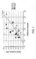
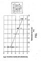
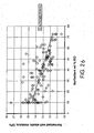

Classifications
-
- C—CHEMISTRY; METALLURGY
- C09—DYES; PAINTS; POLISHES; NATURAL RESINS; ADHESIVES; COMPOSITIONS NOT OTHERWISE PROVIDED FOR; APPLICATIONS OF MATERIALS NOT OTHERWISE PROVIDED FOR
- C09K—MATERIALS FOR MISCELLANEOUS APPLICATIONS, NOT PROVIDED FOR ELSEWHERE
- C09K3/00—Materials not provided for elsewhere
-
- H—ELECTRICITY
- H01—ELECTRIC ELEMENTS
- H01L—SEMICONDUCTOR DEVICES NOT COVERED BY CLASS H10
- H01L21/00—Processes or apparatus adapted for the manufacture or treatment of semiconductor or solid state devices or of parts thereof
- H01L21/02—Manufacture or treatment of semiconductor devices or of parts thereof
- H01L21/02104—Forming layers
- H01L21/02107—Forming insulating materials on a substrate
- H01L21/02109—Forming insulating materials on a substrate characterised by the type of layer, e.g. type of material, porous/non-porous, pre-cursors, mixtures or laminates
- H01L21/02112—Forming insulating materials on a substrate characterised by the type of layer, e.g. type of material, porous/non-porous, pre-cursors, mixtures or laminates characterised by the material of the layer
- H01L21/02123—Forming insulating materials on a substrate characterised by the type of layer, e.g. type of material, porous/non-porous, pre-cursors, mixtures or laminates characterised by the material of the layer the material containing silicon
- H01L21/02126—Forming insulating materials on a substrate characterised by the type of layer, e.g. type of material, porous/non-porous, pre-cursors, mixtures or laminates characterised by the material of the layer the material containing silicon the material containing Si, O, and at least one of H, N, C, F, or other non-metal elements, e.g. SiOC, SiOC:H or SiONC
-
- H—ELECTRICITY
- H01—ELECTRIC ELEMENTS
- H01L—SEMICONDUCTOR DEVICES NOT COVERED BY CLASS H10
- H01L21/00—Processes or apparatus adapted for the manufacture or treatment of semiconductor or solid state devices or of parts thereof
- H01L21/02—Manufacture or treatment of semiconductor devices or of parts thereof
- H01L21/02104—Forming layers
- H01L21/02107—Forming insulating materials on a substrate
- H01L21/02109—Forming insulating materials on a substrate characterised by the type of layer, e.g. type of material, porous/non-porous, pre-cursors, mixtures or laminates
- H01L21/02203—Forming insulating materials on a substrate characterised by the type of layer, e.g. type of material, porous/non-porous, pre-cursors, mixtures or laminates the layer being porous
-
- H—ELECTRICITY
- H01—ELECTRIC ELEMENTS
- H01L—SEMICONDUCTOR DEVICES NOT COVERED BY CLASS H10
- H01L21/00—Processes or apparatus adapted for the manufacture or treatment of semiconductor or solid state devices or of parts thereof
- H01L21/02—Manufacture or treatment of semiconductor devices or of parts thereof
- H01L21/02104—Forming layers
- H01L21/02107—Forming insulating materials on a substrate
- H01L21/02109—Forming insulating materials on a substrate characterised by the type of layer, e.g. type of material, porous/non-porous, pre-cursors, mixtures or laminates
- H01L21/02205—Forming insulating materials on a substrate characterised by the type of layer, e.g. type of material, porous/non-porous, pre-cursors, mixtures or laminates the layer being characterised by the precursor material for deposition
- H01L21/02208—Forming insulating materials on a substrate characterised by the type of layer, e.g. type of material, porous/non-porous, pre-cursors, mixtures or laminates the layer being characterised by the precursor material for deposition the precursor containing a compound comprising Si
- H01L21/02214—Forming insulating materials on a substrate characterised by the type of layer, e.g. type of material, porous/non-porous, pre-cursors, mixtures or laminates the layer being characterised by the precursor material for deposition the precursor containing a compound comprising Si the compound comprising silicon and oxygen
- H01L21/02216—Forming insulating materials on a substrate characterised by the type of layer, e.g. type of material, porous/non-porous, pre-cursors, mixtures or laminates the layer being characterised by the precursor material for deposition the precursor containing a compound comprising Si the compound comprising silicon and oxygen the compound being a molecule comprising at least one silicon-oxygen bond and the compound having hydrogen or an organic group attached to the silicon or oxygen, e.g. a siloxane
-
- H—ELECTRICITY
- H01—ELECTRIC ELEMENTS
- H01L—SEMICONDUCTOR DEVICES NOT COVERED BY CLASS H10
- H01L21/00—Processes or apparatus adapted for the manufacture or treatment of semiconductor or solid state devices or of parts thereof
- H01L21/02—Manufacture or treatment of semiconductor devices or of parts thereof
- H01L21/02104—Forming layers
- H01L21/02107—Forming insulating materials on a substrate
- H01L21/02225—Forming insulating materials on a substrate characterised by the process for the formation of the insulating layer
- H01L21/0226—Forming insulating materials on a substrate characterised by the process for the formation of the insulating layer formation by a deposition process
- H01L21/02282—Forming insulating materials on a substrate characterised by the process for the formation of the insulating layer formation by a deposition process liquid deposition, e.g. spin-coating, sol-gel techniques, spray coating
-
- H—ELECTRICITY
- H01—ELECTRIC ELEMENTS
- H01L—SEMICONDUCTOR DEVICES NOT COVERED BY CLASS H10
- H01L21/00—Processes or apparatus adapted for the manufacture or treatment of semiconductor or solid state devices or of parts thereof
- H01L21/02—Manufacture or treatment of semiconductor devices or of parts thereof
- H01L21/04—Manufacture or treatment of semiconductor devices or of parts thereof the devices having at least one potential-jump barrier or surface barrier, e.g. PN junction, depletion layer or carrier concentration layer
- H01L21/18—Manufacture or treatment of semiconductor devices or of parts thereof the devices having at least one potential-jump barrier or surface barrier, e.g. PN junction, depletion layer or carrier concentration layer the devices having semiconductor bodies comprising elements of Group IV of the Periodic System or AIIIBV compounds with or without impurities, e.g. doping materials
- H01L21/30—Treatment of semiconductor bodies using processes or apparatus not provided for in groups H01L21/20 - H01L21/26
- H01L21/31—Treatment of semiconductor bodies using processes or apparatus not provided for in groups H01L21/20 - H01L21/26 to form insulating layers thereon, e.g. for masking or by using photolithographic techniques; After treatment of these layers; Selection of materials for these layers
- H01L21/312—Organic layers, e.g. photoresist
- H01L21/3121—Layers comprising organo-silicon compounds
- H01L21/3122—Layers comprising organo-silicon compounds layers comprising polysiloxane compounds
-
- H—ELECTRICITY
- H01—ELECTRIC ELEMENTS
- H01L—SEMICONDUCTOR DEVICES NOT COVERED BY CLASS H10
- H01L21/00—Processes or apparatus adapted for the manufacture or treatment of semiconductor or solid state devices or of parts thereof
- H01L21/02—Manufacture or treatment of semiconductor devices or of parts thereof
- H01L21/04—Manufacture or treatment of semiconductor devices or of parts thereof the devices having at least one potential-jump barrier or surface barrier, e.g. PN junction, depletion layer or carrier concentration layer
- H01L21/18—Manufacture or treatment of semiconductor devices or of parts thereof the devices having at least one potential-jump barrier or surface barrier, e.g. PN junction, depletion layer or carrier concentration layer the devices having semiconductor bodies comprising elements of Group IV of the Periodic System or AIIIBV compounds with or without impurities, e.g. doping materials
- H01L21/30—Treatment of semiconductor bodies using processes or apparatus not provided for in groups H01L21/20 - H01L21/26
- H01L21/31—Treatment of semiconductor bodies using processes or apparatus not provided for in groups H01L21/20 - H01L21/26 to form insulating layers thereon, e.g. for masking or by using photolithographic techniques; After treatment of these layers; Selection of materials for these layers
- H01L21/314—Inorganic layers
- H01L21/316—Inorganic layers composed of oxides or glassy oxides or oxide based glass
- H01L21/31695—Deposition of porous oxides or porous glassy oxides or oxide based porous glass
Definitions
- the level of metal impurities present in the material is another consideration in the production of low dielectric materials and the resultant film.
- the film In order for a low dielectric film to be suitable for Integrated Circuit (IC) fabrication, it is desirable that the film has a controlled level of impurities.
- the film should be deposited using ingredients that have minimal levels of nonvolatile impurities that may be harmful in silicon oxide-based insulator films in microelectronic devices.
- alkali metal ions such as sodium and potassium should be excluded from silicon dioxide films used as metal oxide semiconductor (“MOS”) transistor insulators and multilevel interconnection insulators. These positively charged ions might become mobile when exposed to electric fields and drift away from the positively biased film interface and toward the negatively biased film interface causing capacitance-voltage shifts.
- MOS metal oxide semiconductor
- the present invention is directed to low dielectric materials and films comprising same.
- the dielectric materials of the present invention have relatively low metal content and allow for ease of manufacture in comparison to other materials in the art.
- the low dielectric materials and films of the present invention are suitable for use as a "performance material".
- performance material as used herein relates to an inorganic material that is suitable for use as an interlevel dielectric (ILD), or a mesoporous silicon-based material that is suitable for use in semiconductors, semiconductor manufacturing, photonics, nano-scale mechanical or nano-scale electrical devices, gas separations, liquid separations, or chemical sensors.
- ILD interlevel dielectric
- silicon-based silicon-based material that is suitable for use in semiconductors, semiconductor manufacturing, photonics, nano-scale mechanical or nano-scale electrical devices, gas separations, liquid separations, or chemical sensors.
- silicon-based and “silica-based” are used interchangeably throughout the specification.
- the term "monovalent organic group” as used herein relates to an organic group bonded to an element of interest, such as Si or O, through a single C bond, i.e., Si-C or O-C.
- monovalent organic groups include, an alkyl or an aryl group.
- the alkyl group may be a linear, branched, or cyclic alkyl group having from 1 to 5 carbon atoms such as, for example, a methyl, ethyl, propyl, butyl, or pentyl group.
- aryl groups suitable as the monovalent organic group include phenyl, methylphenyl, ethylphenyl and fluorophenyl.
- one or more hydrogens within the alkyl group may be substituted with an additional atom such as a halide atom (i.e., fluorine), or an oxygen atom to give a carbonyl functionality.
- At least one silica source may include compounds that produce a Si-H bond upon elimination, provided they are within the definition of appending claim 7.
- Chemical reagent purification can be performed using common procedures, such as distillation, employment of ion exchange columns, etc.
- chemical reagents with boiling points greater than about 160°C such as surfactants and high boiling point solvents
- the purification process can be conducted wherein the at least chemical reagent to be purified, either neat or dissolved within solvent to provide a solution, is contacted with at least one ion exchange compound.
- the at least one chemical reagent to be purified is contacted with at least one ion exchange compound.
- the mixture may be deposited onto the substrate to form the coated substrate.
- substrate is any suitable composition that is formed before the dielectric film of the present invention is applied to and/or formed on that composition.
- Suitable substrates that may be used in conjunction with the present invention include, but are not limited to, semiconductor materials such as gallium arsenide ("GaAs"), silicon, and compositions containing silicon such as crystalline silicon, polysilicon, amorphous silicon, epitaxial silicon, silicon dioxide (“SiO 2 "), and mixtures thereof.
- GaAs gallium arsenide
- silicon silicon
- compositions containing silicon such as crystalline silicon, polysilicon, amorphous silicon, epitaxial silicon, silicon dioxide (“SiO 2 ")
- the mixture may be applied onto the substrate via a variety of methods including, but not limited to, dipping, rolling, brushing, spraying, or spin coating.
- the materials and films of the invention may be mesoporous.
- the term "mesoporous”, as used herein, describes pore sizes that range from about 1 nm (10 ⁇ ) to about 50 nm (500 ⁇ ), preferably from about 7 nm (10 ⁇ ) to about 10 nm (100 ⁇ ), and most preferably from about 1 nm (10 ⁇ ) to about 5 nm (50 ⁇ ). It is preferred that the film have pores of a narrow size range and that the pores are homogeneously distributed throughout the film. Films of the invention preferably have a porosity of about 10% to about 90%. The porosity of the films may be closed or open pore.
- the solution was dispensed onto a low resistivity P type ⁇ 100> Si wafer spinning at 500 rpm for 7 seconds to spread the formulation across the wafer and then accelerated to 1800 rpm for 35-40 seconds to evaporate the solvents and dry the film.
- the film formed during the spin coating process was then heated on a hot plate at 90°C for 90 seconds, 180°C for 90 seconds, and 400°C for 180 seconds in an air or nitrogen atmosphere to remove the porogen.
- the wafer was cooled under ambient conditions.
- the properties of each film are provided in Table V. Examples 9 through 11 reconfirm the array results of the effect of the carboxylate, the weight percent EO, and the pAcid values of the mixture have on the normalized wall elastic modulus.
Abstract
Description
- The present invention relates generally to a material suitable for use, for example, in electronic devices. More specifically, the invention relates to a composition for making a low dielectric performance material or film comprising same having an improved elastic modulus and a low dielectric constant.
- There is a continuing desire in the microelectronics industry to increase the circuit density in multilevel integrated circuit devices such as memory and logic chips in order to improve the operating speed and reduce power consumption. In order to continue to reduce the size of devices on integrated circuits, it has become necessary to use insulators having a low dielectric constant to reduce the resistance-capacitance ("RC") time delay of the interconnect metallization and to prevent capacitive cross talk between the different levels of metallization. Such low dielectric materials are desirable for premetal dielectric layers and interlevel dielectric layers.
- Typical dielectric materials for devices with 180 nm line width are materials with a dielectric constant between about 3.8 and 4.2. As the line width decreases, the dielectric constant should also be decreased. For example, devices with 130 nm line width require materials with a dielectric constant between about 2.5 and 3.0. Extremely low dielectric constant ("ELK") materials generally have a dielectric constant between about 2.0 and 2.5. Devices with 90 nm line width require materials with dielectric constants less than 2.4. According to the 2001 International Technology roadmap for Semiconductors (ITRS) interconnect roadmap, the projected dielectric constant requirements for interlevel metal insulators will be less than 2.1 for the 65 nm node, less than 1.9 for the 45 nm node, less than 1.7 for the 32 nm node, and less than 1.6 for the 22 nm node.
- A number of processes have been used for preparing low dielectric constant films. Chemical vapor deposition (CVD) and spin-on dielectric (SOD) processes are typically used to prepare thin films of insulating layers. Other hybrid processes are also known such as CVD of liquid polymer precursors and transport polymerization CVD. A wide variety of low κ materials deposited by these techniques have been generally classified in categories such as purely inorganic materials, ceramic materials, silica-based materials, purely organic materials, or inorganic-organic hybrids. Likewise, a variety of processes have been used for curing these materials to decompose and/or remove volatile components and substantially crosslink the films such as heating, treating the materials with plasmas, electron beams, or UV radiation.
- Since the dielectric constant of air is nominally 1.0, one approach to reducing the dielectric constant of a material may be to introduce porosity. Porosity has been introduced in low dielectric materials through a variety of different means. A dielectric film when made porous may exhibit lower dielectric constants compared to a dense film, however, the elastic modulus of the film generally decreases with increasing porosity. Consequently, it may be impractical to use these low dielectric compositions due to the trade-off in dielectric constant with elastic modulus.
- The dielectric constant (κ) of a material generally cannot be reduced without a subsequent reduction in the mechanical properties, i.e., modulus, hardness, etc., of the material. Mechanical strength is needed for subsequent processing steps such as etching, CMP ("Chemical Mechanical Planarization"), and depositing additional layers such as diffusion barriers for copper, copper metal ("Cu"), and cap layers on the product. In some of these processes, temperature cycling of multiple layers may induce stresses due to the thermal coefficient of expansion mismatch between the different materials thereby causing cracking or delamination. Surface planarity is also required and may be maintained through controlling processing parameters such as those during the film formation process and also through CMP. Mechanical integrity, or stiffness, compressive, and shear strengths, may be particularly important to survive CMP. It has been found that the ability to survive CMP may be correlated with the elastic, or Young's, modulus of the material, along with other factors including polishing parameters such as the down force and platen speed. See, for example, Wang et al., "Advanced processing: CMP of Cu/low-κ and Cu/ultralow-K layers", Solid State Technol., September, 2001; Lin et al., "Low- κ Dielectrics Characterization for Damascene Integration", International Interconnect Technology Conference, Burlingame, CA, June, 2001. These mechanical properties are also important in the packaging of the final product.
- Another consideration in the production of low dielectric materials and the resultant film is the level of metal impurities present in the material. In order for a low dielectric film to be suitable for Integrated Circuit (IC) fabrication, it is desirable that the film has a controlled level of impurities. In other words, the film should be deposited using ingredients that have minimal levels of nonvolatile impurities that may be harmful in silicon oxide-based insulator films in microelectronic devices. In the IC industry, it is well known that alkali metal ions such as sodium and potassium should be excluded from silicon dioxide films used as metal oxide semiconductor ("MOS") transistor insulators and multilevel interconnection insulators. These positively charged ions might become mobile when exposed to electric fields and drift away from the positively biased film interface and toward the negatively biased film interface causing capacitance-voltage shifts.
- Some commercially available chemical reagents used in the production of low dielectric films contain alkali metal impurities. These impurities may result from residual levels of catalyst used in the manufacture of the chemical precursor reagents. Ratios of 0.005-0.05:1 mol of NaOH, KOH, or NaOCH3 to alcohol are frequently used in the base-catalyzed ethoxylation of aliphatic alcohols, alkylphenols, and fatty acids. See, e.g., Lynn et al.,"Surfactants", Kirk-Othmer Encyclopedia of Chemical Technology, John Wiley & Sons, Inc., (1997). For example, the use of 0.005 mol NaOH per mol of alcohol in the production of TRITON™ X-114, an alkylphenol ethoxylate with an average 7.5 moles of ethoxylate per mole of alcohol, may result in 214 ppm of sodium in the final product. Such levels of residual catalytic impurities are often of little consequence in typical applications of these chemicals because the surfactant is often used at such low levels that the catalytic impurities imparted by the surfactant become insignificant in the final formulation. A polymer such as polyethylene glycol (PEG) may be made using different catalyst systems depending on the desired molecular weight. For molecular weight below 20,000, base or the Na+ or K+ alkoxides of methanol or butanol are used as the catalyst. See, for instance, Glass, J. E. "Water-Soluble Polymers", Kirk-Othmer Encyclopedia of Chemical Technology, John Wiley & Sons, Inc. (1988). Solvents, like surfactants, can also contain residual catalytic impurities. For instance, the formation of ethers, such as propylene glycol propyl ether (PGPE), through the reaction of propylene oxide with an alcohol, is often base-catalyzed when high selectivity to the primary alkyl ether over the secondary ether is desired which can result in residual impurities. See, for instance, Brown, et al., "Glycols: Ethylene Glycol and Propylene Glycol", Kirk-Othmer Encyclopedia of Chemical Technology, 3rd ed., John Wiley & Sons, N.Y., (1980), Vol. 11, p 953. A further source of impurities may result from an inattention to detail, such as packaging or handling outside a clean room, because such stringent purity requirements are not needed for typical applications.
- Alkali metal impurity specifications for chemical precursor solutions for integrated circuit applications typically set the allowable impurity levels to approximately 20 parts per billion maximum for each type of alkali metal and less than 50 ppb total. To meet these limits, the material supplier to the IC industry may purify the surfactants. The reference,
EP 1,142,832 , assigned to the assignee of the present application, discusses how the dielectric and mechanical properties of the resulting films may be adversely affected by the purification of surfactants used as porogens in the film-forming mixture. The reference,US 2002/0045693 , discusses how the dielectric properties of the resulting films may be adversely affected by the purification of reagents even if surfactant is not present. - The following references,
U.S. Pat. Nos. 6,406,794 ,6,329,017 ,6,495,479 ,6,126,733 ,U. S. Pat. App. Serial No. 2002/0189495 ,EP 1123753 , and Chem. Mater. 2001 13, 2762 and 1848, provide various compositions used for forming dielectric films that include chemical reagents such as at least one source for silicon, a porogen, and a solvent. These references fail to disclose the purification of the chemical reagents, particularly porogens, prior to addition to the composition to remove alkali metal impurities. Some references, such asU. S. Pat. No. 6,376,634 and6,126,733 , discuss purifying the reagents prior to addition to the composition. However, as mentioned previously, in certain instances the purification process may adversely affect the dielectric constant and/or mechanical properties of the material. - Accordingly, there is a need in the art to provide improved dielectric materials having low dielectric constant and sufficient mechanical strength. To achieve that end, there is also a need in the art to provide a means to correlate dielectric constant, porosity, and elastic modulus to identify and develop low dielectric materials. There is also a need in the art to provide dielectric materials and films that have relatively low metal content yet still maintain the beneficial properties, i.e., lower κ and higher modulus, that high levels of metals may impart. Further, there is a need in the art to provide processes for making low dielectric films at relatively low temperatures and relatively short cycle times.
- The present invention satisfies some, if not all of the needs in the art by providing improved performance materials and films comprising same, preferably having a dielectric constant of 3.7 or below, yet sufficient mechanical strength. The invention is defined by the features of the independent claims. Specific embodiments are defined in the dependent claims.
- These and other aspects of the invention will become apparent from the following detailed description.
- FIG. 1 provides a plot of elastic modulus vs. dielectric constant for materials of the present invention having a normalized wall elastic modulus greater than 16 GPa and using MTAS as the hydrophobic silica source compared to materials having a normalized wall elastic modulus less than 16 GPa and using MTES as the hydrophobic silica source
- FIGs. 2a and 2b illustrate the effect of weight percent ethylene oxide groups for single surfactants and mixtures of surfactants, respectively, on the normalized wall elastic modulus on the materials of the present invention.
- FIG. 3 provides a plot of materials of the present invention that illustrates that higher pAcid levels may result in a higher normalized wall elastic modulus.
- The present invention is directed to low dielectric materials and films comprising same. The dielectric materials of the present invention have relatively low metal content and allow for ease of manufacture in comparison to other materials in the art. The low dielectric materials and films of the present invention are suitable for use as a "performance material". The term "performance material" as used herein relates to an inorganic material that is suitable for use as an interlevel dielectric (ILD), or a mesoporous silicon-based material that is suitable for use in semiconductors, semiconductor manufacturing, photonics, nano-scale mechanical or nano-scale electrical devices, gas separations, liquid separations, or chemical sensors. The terms "silicon-based" and "silica-based" are used interchangeably throughout the specification.
- In certain preferred embodiments, the dielectric or performance material of the present invention may have improved mechanical and other properties as a result of the selecting the weight percentage of ethoxylation in the porogen. The improvement in properties may be expressed by the normalized wall elastic modulus (E0'). Pending
U. S. Pat. Application Serial No. 10/158,511 , discusses the normalized wall elastic modulus (E0') and its relationship on the material properties. Two measured attributes of a low dielectric material, dielectric constant and elastic modulus, are correlated into one figure of merit, the normalized wall elastic modulus (E0'), that can be used to identify and develop improved low dielectric materials. Improved dielectric materials are materials having a low dielectric constant yet high enough elastic modulus to tolerate subsequent processing steps such as packaging and CMP processes. In this connection, materials with substantially identical normalized wall elastic modulus values belong to a family of materials whose dielectric constant and elastic modulus can be adjusted by varying the porosity. Thus, once an improved dielectric material is identified, i.e. one with a higher normalized wall elastic modulus, the target dielectric constant can be obtained by varying the porosity. - The term "normalized wall elastic modulus", as used herein, is the wall elastic modulus of a material that is normalized to a wall with a dielectric constant of 4.2, which is the dielectric constant of a SiO2 dense oxide material. Once the dielectric constant (κ) and the elastic modulus (E) of a material are measured, the normalized wall elastic modulus (E0') can be calculated. The E0' of the material is calculated using Maxwell's relationship for mixed dielectrics applied to porous materials, the measured value for dielectric constant (κ), a wall κSiO2 of 4.2, Day's 2-d circular hole model for elastic modulus extended to 3-d cylindrical pores with the modulus measured perpendicular to the pore axes, and the measured value for E. While the derivation for the normalized wall elastic modulus is based upon cylindrical pores in the extension of the Day model and spherical inclusions in the Maxwell model, it is anticipated that other types and forms or porosity, i.e., non-cylindrical, open porosity, closed porosity, etc., would fall within the scope of the present invention.
- A void fraction value is first calculated from the Maxwell equation using the observed value for κ of the material and a value for the wall κ of 4.2, corresponding to the dielectric constant of dense, amorphous silica. The dielectric constant of the material is preferably less than 4.2 since κSiO2 is 4.2. The Maxwell equation was rearranged to solve for porosity or void fraction, as a function of measured κ and wall κ, as provided in Equation (1):

where: - κSiO2 = 4.2
- χp = void fraction value
- κ = measured value of dielectric constant
- The normalized wall elastic modulus may then be calculated based on Day's 2-d circular hole model for elastic modulus using Equation (2). The equation is valid for void fractions less than qc, the critical porosity at which the pores touch, and beyond which the modulus is predicted to be zero. For materials with a wall κ of 4.2, this determines a minimum κ value = 1.23 for composites with E > 0.
Day et al. 2-d circular hole model:
where - q = void fraction
- qc = 0.9069 = percolation threshold, void fraction at which circles overlap and modulus goes to zero
- ql = 1/3 = initial slope
- m = 1.5 = critical exponent
- α = -0.251 = parameter to get correct critical amplitude
- θ = -1.83 = free fitting parameter
- The Day 2-d circular hole model for elastic modulus is extended to 3-d cylindrical pores with the modulus measured perpendicular to the pore axes as provided in the Equation (3). The normalized wall elastic modulus can be calculated using the calculated void fraction value from Equation (1), the elastic modulus for 2-d circular holes from Equation (2), the observed value for E, and a value for Poisson's ratio (ν) of 0.25.
3-d extension perpendicular to the cylinders:
where - ν = Poisson's ratio = 0.25
- q = void fraction
- E0 = wall elastic modulus
- When q is set equal to the void fraction value χp obtained from the measured value of κ and Equation (1), and


- The material of the present invention may be formed into a film from a precursor composition or mixture using a variety of different methods. Some examples of processes that may be used to form the film include plasma enhanced chemical vapor deposition ("PECVD"), high density PECVD, photon assisted CVD, plasma-photon assisted CVD ("PPECVD"), CVD of a liquid polymer precursor, or transport polymerization ("TP").
U. S. Pat. Nos. 6,171,945 and6,054,206 provide some exemplary CVD methods that may be used with the present invention. Other processes that can be used to form the film include spin-on deposition methods. In certain embodiments of the present invention, non-contact induced spreading forces such as the process described in pending U.S. Pat. Application Attorney's Docket 2001-030 - SMX 3122 entitled "Apparatus and Methods for Forming Films on Substrates", may be used to apply the mixture, which is incorporated herein by reference in its entirety. Further related processes may be used to apply the mixture include oscillating non-contact induced spreading forces, gravity-induced spreading forces, wetting-induced spreading forces, or combinations thereof. - The materials of the present invention preferably comprise silica. The term "silica", "silica based", or "silica containing", as used herein, is a material that has silicon (Si) and oxygen (O) atoms, and possibly additional substituents such as, but not limited to, other elements such as H, B, C, P, or halide atoms or organic groups such as alkyl groups or aryl groups. In certain preferred embodiments, the material may further comprise silicon-carbon bonds having a total number of Si-C bonds to the total number of Si atoms ranging from between 20 to 80 mole percent, and more preferably from between 40 to 60 mole percent.
- The film of the present invention is preferably formed from a mixture. The mixture may be prepared prior to forming the film or the mixture may form during at least a portion of the film forming process. Depending upon the film formation method, the mixture may be deposited onto a substrate as a liquid, vapor, gas, or aerosol of the mixture.
- The mixture generally comprises an at least one silica source and at least one porogen according to
claim 1. The mixture may further include other constituents such as, but not limited to, water, solvent(s), catalyst, and/or ionic additives. The weight ratio of weight of porogen to the weight of porogen and weight of SiO2 ranges from 0.9 to 0.1. The preferred range may vary depending the desired dielectric constant of the material produced from the mixture because the dielectric constant of the material is inversely proportional to the weight ratio of the porogen. The weight of SiO2 is calculated from the total number of moles of silicon introduced by the silica sources within the mixture. This is not meant to imply that the silica sources are completely converted to SiO2. The weight ratio of solvent to silica is about 30:1 wherein the solvent may include water. The weight ratio of ionic additive to weight of porogen is 0.5 to 0. The molar ratio of R, or organic constituents, to Si ranges from 0.2 to 0.8. The molar ratio of water to OR, where OR is an organic group bonded to silicon through an oxygen atom, e.g. ethoxy functionality on TEOS, ranges from 40 to 1. - The mixture employs chemicals that meet the requirements of the electronics industry because they do not contain contaminants, which reduce the efficiency of preparation of-integrated circuits. Constituents like halogen-containing mineral acids, cationic surfactants with halide counter ions, and anionic surfactants with alkali metal counter ions are preferably avoided in the mixture because they may contribute undesirable counter ions to the materials of the invention. The mixtures of the present invention preferably contain contaminating metals in amounts less than 1 parts per million ("ppm"), preferably less than 200 parts per billion ("ppb"), and more preferably less than 50 ppb. Consequently, materials of the invention may preferably contain contaminating metals in amounts less than 1 parts per million ("ppm"), preferably less than 200 parts per billion ("ppb"), and more preferably less than 50 ppb. Materials of the invention preferably contain contaminating halides in amounts less than 1 ppm, preferably less than 750 ppb, and more preferably less than 500 ppb. The chemical reagents within the mixture contain contaminating metals in amounts less than-1 parts per million ("ppm"); preferably less than 200 parts per billion ("ppb"), and more preferably less than 50 ppb. In certain preferred embodiments, if the chemical reagent contains 1 ppm or greater of contaminating metals, the chemical reagent may be purified prior to addition to the mixture.
- As mentioned previously, the mixture comprises at least one silica source according to appending
claim 1. Other sources of silica may also be present. A "silica source", as used herein, is a compound having silicon (Si) and oxygen (O) and additional substituents such as, but not limited to, other elements such as H, B, C, P, or halide atoms and organic groups such as alkyl groups; or aryl groups. The term "alkyl" as used herein includes linear, branched, or cyclic alkyl.groups, containing from 1 to 24 carbon atoms, preferably from 1 to 12 carbon atoms, and more preferably from 1 to 5 carbon atoms. This term applies also to alkyl moieties contained in other groups such as haloalkyl, alkaryl, or aralkyl. The term "alkyl" further applies to alkyl moieties that are substituted, for example with carbonyl functionality. The term "aryl" as used herein six to twelve member carbon rings having aromatic character. The term "aryl" also applies to aryl moieties that are substituted. The silica source may include materials that have a high number of Si-O bonds, but can further include Si-O-Si bridges, Si-R-Si bridges, Si-C bonds, Si-H bonds, Si-F bonds, or C-H bonds. It is preferred that the at least one silica source imparts a minimum of Si-OH bonds in the dielectric material. - The following are non-limiting examples of silica sources suitable for use in the mixture and method of the present invention. In the chemical formulas which follow and in all chemical formulas throughout this document, the term "independently" should be understood to denote that the subject R group is not only independently selected relative to other R groups bearing different superscripts, but is also independently selected relative to any additional species of the same R group. For example, in the formula RaSi(OR1)4-aSi, when a is 2, the two R groups need not be identical to each other or to R1.
- The term "monovalent organic group" as used herein relates to an organic group bonded to an element of interest, such as Si or O, through a single C bond, i.e., Si-C or O-C. Examples of monovalent organic groups include, an alkyl or an aryl group. The alkyl group may be a linear, branched, or cyclic alkyl group having from 1 to 5 carbon atoms such as, for example, a methyl, ethyl, propyl, butyl, or pentyl group. Examples of aryl groups suitable as the monovalent organic group include phenyl, methylphenyl, ethylphenyl and fluorophenyl. In certain embodiments, one or more hydrogens within the alkyl group may be substituted with an additional atom such as a halide atom (i.e., fluorine), or an oxygen atom to give a carbonyl functionality.
- In certain embodiments, an additional silica source may be represented by the following formula: RaSi(OR1)4-a, wherein R independently represents a hydrogen atom, a fluorine atom, or a monovalent organic group; R1 independently represents a monovalent organic group; and a is an integer ranging from 1 to 2. Specific examples of the compounds represented by RaSi(OR1)4-a include: methyltrimethoxysilane, methyltriethoxysilane, methyltri-n-propoxysilane, methyltri-iso- propoxysilane, methyltri-n-butoxysilane, methyltri-sec-butoxysilane, methyltri-tert-butoxysilane, methyltriphenoxysilane, ethyltrimethoxysilane, ethyltriethoxysilane, ethyltri-n-propoxysilane, ethyltri-iso-propoxysilane, ethyltri-n-butoxysilane, ethyltri-sec-butoxysilane, ethyltri-tert-butoxysilane, ethyltriphenoxysilane, n-propyltrimethoxysilane, n-propyltriethoxysilane, n-propyltri-n- propoxysilane, n-propyltri-iso-propoxysilane, n-propyltin-n-butoxysilane, n-propyltri-sec-butoxysilane, n-propyltri-tert-butoxysilane, n-propyltriphenoxysilane, isopropyltrimethoxysilane, isopropyltriethoxysilane, isopropyltri-n-propoxysilane, isopropyltriisopropoxysilane, isopropyltri-n-butoxysilane, isopropyltri-sec-butoxysilane, isopropyltri-tert-butoxysilane, isopropyltriphenoxysilane, n-butyltrimethoxysilane, n-butyltriethoxysilane, n-butyltri-n-propoxysilane, n-butyltriisopropoxysilane, n-butyltri-n-butoxysilane, n-butyltri-sec-butoxysilane, n-butyltri-tert-butoxysilane, n-butyltriphenoxysilane; sec-butyltrimethoxysilane, sec-butyltriethoxysilane, sec-butyltri-n-propoxysilane, sec-butyltriisopropoxysilane, sec-butyltri-n-butoxysilane, sec-butyltri-sec-butoxysilane, sec-butyltri-tert-butoxysilane, sec-butyltriphenoxysilane, tert-butyltrimethoxysilane, tert-butyltriethoxysilane, tert-butyltri-n-propoxysilane, tert-butyltriisopropoxysilane, tert-butyltri-n-butoxysilane, tert-butyltri-sec-butoxysilane, tert-butyltri-tert-butoxysilane, tert-butyltriphenoxysilane, isobutyltrimethoxysilane, isobutyltriethoxysilane, isobutyltri-n-propoxysilane, isobutyltriisopropoxysilane, isobutyltri-n-butoxysilane, isobutyltri-sec-butoxysilane, isobutyltri-tert-butoxysilane, isobutyltriphenoxysilane, n-pentyltrimethoxysilane, n-pentyltriethoxysilane, n-pentyltri-n-propoxysilane, n-pentyltriisopropoxysilane, n-pentyltri-n-butoxysilane, n-pentyltri-sec-butoxysilane, n-pentyltri-tert-butoxysilane, n-pentyltriphenoxysilane; sec-pentyltrimethoxysilane, sec-pentyltriethoxysilane, sec-pentyltri-n-propoxysilane, sec-pentyltriisopropoxysilane, sec-pentyltri-n-butoxysilane, sec-pentyltri-sec-butoxysilane, sec-pentyltri-tert-butoxysilane, sec-pentyltriphenoxysilane, tert-pentyltrimethoxysilane, tert-pentyltriethoxysilane, tert-pentyltri-n-propoxysilane, tert-pentyltriisopropoxysilane, tert-pentyltri-n-butoxysilane, tert-pentyltri-sec-butoxysilane, tert-pentyltri-tert-butoxysilane, tert-pentyltriphenoxysilane, isopentyltrimethoxysilane, isopentyltriethoxysilane, isopentyltri-n-propoxysilane, isopentyltriisopropoxysilane, isopentyltri-n-butoxysilane, isopentyltri-sec-butoxysilane, isopentyltri-tert-butoxysilane, isopentyltriphenoxysilane, neo-pentyltrimethoxysilane, neo-pentyltriethoxysilane, neo-pentyltri-n-propoxysilane, neo-pentyltriisopropoxysilane, neo-pentyltri-n-butoxysilane, neo-pentyltri-sec-butoxysilane, neo-pentyltri-neo-butoxysilane, neo-pentyltriphenoxysilane phenyltrimethoxysilane, phenyltriethoxysilane, phenyltri-n-propoxysilane, phenyltriisopropoxysilane, phenyltri-n-butoxysilane, phenyltri-sec-butoxysilane, phenyltri-tert-butoxysilane, phenyltriphenoxysilane, δ-trifluoropropyltrimethoxysilane, δ-trifluoropropyltriethoxysilane, dimethyldimethoxysilane, dimethyldiethoxysilane, dimethyldi-n-propoxysilane, dimethyldiisopropoxysilane, dimethyldi-n-butoxysilane, dimethyldi-sec-butoxysilane, dimethyldi-tert-butoxysilane, dimethyldiphenoxysilane, diethyldimethoxysilane, diethyldiethoxysilane, diethyldi-n-propoxysilane, diethyldiisopropoxysilane, diethyldi-n-butoxysilane, diethyldi-sec-butoxysilane, diethyldi-tert-butoxysilane, diethyldiphenoxysilane, di-n-propyldimethoxysilane, di-n-propyldimethoxysilane, di-n-propyldi-n-propoxysilane, di-n-propyldiisopropoxysilane, di-n-propyldi-n-butoxysilane, di-n-propyldi-sec-butoxysilane, din-propyldi-tert-butoxysilane, di-n-propyldiphenoxysilane, diisopropyldimethoxysilane, diisopropyldiethoxysilane, diisopropyldi-n-propoxysilane, diisopropyldiisopropoxysilane, diisopropyldi-n-butoxysilane, diisopropyldi-sec-butoxysilane, diisopropyldi-tert-butoxysilane, diisopropyldiphenoxysilane, di-n-butyldimethoxysilane, di-n-butyldiethoxysilane, di-n-butytdi-n-propoxysilane, di-n- butyldiisopropoxysilane, di-n-butyldi-n-butoxysilane, di-n-butyldi-sec-butoxysilane, di-n-butyldi-tert-butoxysilane, di-n-butyldiphenoxysilane, di-sec-butyidimethoxysilane, di-sec-butyldiethoxysilane, di-sec-butyldi-n-propoxysilane, di-sec-butyldiisopropoxysilane, di-sec-butyldi-n-butoxysilane, di-sec-butyldi-sec-butoxysilane, di-sec-butyldi-tert-butoxysilane, di-sec-butyldiphenoxysilane, di-tert-butyldimethoxysilane, di-tert-butyldiethoxysilane, di-tert-butyldi-n-propoxysilane, di-tert-butyldiisopropoxysilane, di-tert-butyldi-n-butoxysilane, di-tert-butyldi-sec-butoxysilane, di-tert-butyldi-tert-butoxysilane, di-tert-butyldiphenoxysilane, diphenyldimethoxysilane, diphenyldiethoxysilane, diphenyldi-n-propoxysilane, diphenyldiisopropoxysilane, diphenyldi-n-butoxysilane, diphenyldi-sec-butoxysilane, diphenyldi-tert-butoxysilane, diphenyldiphenoxysilane, methylneopentyldimethoxysilane, methylneopentyldiethoxysilane, methyldimethoxysilane, ethyldimethoxysilane, n-propyldimethoxysilane, isopropyldimethoxysilane, n-butyldimethoxysilane, sec-butyldimethoxysilane, tert-butyldimethoxysilane, isobutyldimethoxysilane, n-pentyldimethoxysilane, sec-pentyldimethoxysilane, tert-pentyldimethoxysilane, isopentyldimethoxysilane, neopentyldimethoxysilane, neohexyldimethoxysilane, cyclohexyldimethoxysilane, phenyldimethoxysilane, methyldiethoxysilane, ethyldiethoxysilane, n-propyldiethoxysilane, isopropyldiethoxysilane, n-butyldiethoxysilane, sec-butyldiethoxysilane, tert-butyidiethoxysilane, isobutyldiethoxysilane, n-pentyldiethoxysilane, sec-pentyldiethoxysilane, tert-pentyldiethoxysilane, isopentyldiethoxysilane, neopentyldiethoxysilane, neohexyldiethoxysilane, cyclohexyldiethoxysilane, phenyldiethoxysilane,; trimethoxysilane, triethoxysilane, tri-n-propoxysilane, triisopropoxysilane, tri-n-butoxysilane, tri-sec-butoxysilane, tri-tert-butoxysilane, triphenoxysilane. Of the above compounds, the preferred compounds are methyltrimethoxysilane, methyltriethoxysilane, methyltri-n-propoxysilane, methyltriisopropoxysilane, ethyltrimethoxysilane, ethyltriethoxysilane, dimethyldimethoxysilane, dimethyldiethoxysilane, diethyldimethoxysilane, and diethyldiethoxysilane.
- An additional silica source may be a compound having the formula Si(OR2)4 wherein R2 independently represents a monovalent organic group. Specific examples of the compounds represented by Si(OR2)4 include tetramethoxysilane, tetraethoxysilane, tetra-n-propoxysilane, tetraisopropoxysilane tetra-n-butoxysilane, tetra-sec-butoxysilane, tetra- tert-butoxysilane, tetraacetoxysilane, and tetraphenoxysilane. Of the above, the preferred compounds are tetramethoxysilane, tetraethoxysilane, tetra-n-propoxysilane, or tetraisopropoxysilane, tetraphenoxysilane.
- An additional silica source may be a compound having the formula R3 b(R4O)3-bSi-(R7)-Si(OR5)3-cR6 c, wherein R3 and R6 are independently a hydrogen atom, a fluorine atom, or a monovalent organic group; R4 and R5 are independently a monovalent organic group; b and c may be the same or different and each is a number ranging from 0 to 2; R7 is an oxygen atom, a phenylene group, or a group represented by -(CH2)n-, wherein n is an integer ranging from 1 to 6; or combinations thereof. Specific examples of these compounds wherein R7 is an oxygen atom include: hexamethoxydisiloxane, hexaethoxydisiloxane, hexaphenoxydisiloxane, 1,1,1,3,3-pentamethoxy-3- methyldisiloxane, 1,1,1,3,3-pentaethoxy-3-methyldisiloxane, 1,1,1,3,3-pentamethoxy-3-phenyldisiloxane, 1,1,1,3,3-pentaethoxy-3-phenyldisiloxane, 1,1,3,3-tetramethoxy-1,3-dimethyldisiloxane, 1,1,3,3-tetraethoxy-1,3-dimethyldisiloxane, 1,1,3,3-tetramethoxy-1,3-diphenyldisiloxane, 1,1,3,3-tetraethoxy-1,3-diphenyldisiloxane, 1,1,3-trimethoxy-1,3,3-trimethyldisiloxane, 1,1,3-triethoxy-1,3,3-trimethyldisitoxane, 1,1,3-trimethoxy-1,3,3-triphenyldisiloxane, 1,1,3-triethoxy-1,3,3-triphenyldisiloxane, 1,3-dimethoxy-1,1,3,3-tetramethyldisiloxane, 1,3-diethoxy-1,1,3,3-tetramethyldisiloxane, 1,3-dimethoxy-1,1,3,3-tetraphenyldisiloxane and 1,3-diethoxy-1,1,3,3-tetraphenyldisiloxane. Of those, preferred compounds are hexamethoxydisiloxane, hexaethoxydisiloxane, hexaphenoxydisiloxane, 1,1,3,3-tetramethoxy-1,3-dimethyldisiloxane, 1,1,3,3-tetraethoxy-1,3-dimethyldisiloxane, 1,1,3,3-tetramethoxy-1,3-diphenyldisiloxane, 1,3-dimethoxy-1,1,3,3-tetramethyldisiloxane, 1,3-diethoxy-1,1,3,3-tetramethyldisiloxane, 1,3-dimethoxy-1,1,3,3-tetraphenyldisiloxane;1,3-diethoxy-1,1,3,3-tetraphenyldisiloxane. Specific examples of these compounds wherein R7 is a group represented by -(CH2)n-include: bis(trimethoxysilyl)methane, bis(triethoxysilyl)methane, bis(triphenoxysilyl)methane, bis(dimethoxymethylsilyl)methane, bis(diethoxymethylsilyl)methane, bis(dimethoxyphenylsilyl)methane, bis(diethoxyphenylsilyl)methane, bis(methoxydimethylsilyl)methane, bis(ethoxydimethylsilyl)methane, bis(methoxydiphenylsilyl)methane, bis(ethoxydiphenylsilyl)methane, 1,2-bis(trimethoxysilyl)ethane, 1,2-bis(triethoxysilyl)ethane, 1,2-bis(triphenoxysilyl)ethane, 1,2-bis(dimethoxymethylsilyl)ethane, 1,2-bis(diethoxymethylsilyl)ethane, 1,2-bis(dimethoxyphenylsilyl)ethane, 1,2-bis(diethoxyphenylsilyl)ethane, 1,2-bis(methoxydimethylsilyl)ethane, 1,2-bis(ethoxydimethylsilyl)ethane, 1,2-bis(methoxydiphenylsilyl)ethane, 1,2-bis(ethoxydiphenylsilyl)ethane, 1,3-bis(trimethoxysilyl)propane, 1,3-bis(triethoxysilyl)propane, 1,3-bis(triphenoxysilyl)propane, 1,3-bis(dimethoxymethylsilyl)propane, 1,3-bis(diethoxymethylsilyl)propane, 1,3-bis(dimethoxyphenylsilyl)propane, 1,3-bis(diethoxyphenylsilyl)propane, 1,3-bis(methoxydimethylsilyl)propane, 1,3-bis(ethoxydimethylsilyl)propane, 1,3-bis(methoxydiphenylsilyl)propane; 1,3-bis(ethoxydiphenylsilyl) propane;. Of those, preferred compounds are bis(trimethoxysilyl)methane, bis(triethoxysilyl)methane, bis(dimethoxymethylsilyl)methane, bis(diethoxymethylsilyl)methane, bis(dimethoxyphenylsilyl)methane, bis(diethoxyphenylsilyl)methane, bis(methoxydimethylsilyl)methane, bis(ethoxydimethylsilyl)methane, bis(methoxydiphenylsilyl)methane and bis(ethoxydiphenylsilyl)methane.
- According to the present invention, R1 of the formula RaSi(OR1)4-a; R2 of the formula Si(OR2)4; and R4 and/or R5 of the formula R3 b(R4O)3-bSi-(R7)-Si(OR5)3-cR6 c can each independently be a monovalent organic group of the formula:

- Other examples of the at least one silica source may include a fluorinated silane or fluorinated siloxane such as those provided in U. S.
Pat. No. 6,258,407 , provided they are within the definition according to appendingclaim 1. - Another example of at least one silica source may include compounds that produce a Si-H bond upon elimination, provided they are within the definition of appending claim 7.
- Still further examples of the at least one silica source are found in the non-hydrolytic chemistry methods described, for example, in the references Hay et al., "Synthesis of Organic-Inorganic Hybrids via the Non-hydrolytic Sol-Gel Process", Chem. Mater., 13, 3396-3403 (2001) or Hay, et al., "A Versatile Route to Organically-Modified Silicas and Porous Silicas via the Non-Hydrolytic Sol-Gel Process", J. Mater. Chem., 10, 1811-1818 (2000), provided they are within the definition of appending
claim 1. - Yet another example of an additional silica source may include colloidal silica, fumed silica, or silicic acid starting materials.
- Still other examples of additional silica sources include silsesquioxanes such as hydrogen silsesquioxanes (HSQ, HSiO1.5) and methyl silsesquioxanes (MSQ, RSiO1.5 where R is a methyl group).
- In certain preferred embodiments, the at least one silica source may preferably have an at least one carboxylic acid ester bonded to the Si atom. In addition to the at least one silica source wherein the silica source has at least one Si atom having an carboxylate group attached thereto, the mixture may further comprise additional silica sources that may not necessarily have the carboxylate attached to the Si atom.
- In preferred embodiments, a combination of hydrophilic and hydrophobic silica sources is used in the mixture. In preferred embodiments, the ratio of hydrophobic silica source to the total amount of silica source is greater than about 0.2 molar ratio, preferably from 0.2 to 0.8 molar ratio. The term "hydrophilic", as used herein, refers to compounds wherein the silicon atom can crosslink through at least four bonds: Some examples of hydrophilic sources include alkoxysilanes having an alkoxy functionality and can at least partially crosslink, i.e. a Si atom with four methoxy, ethoxy, propoxy, acetoxy, etc. groups, or materials with carbon or oxygen bonds between Si atoms and all other functionality on the Si atoms being an alkoxide. If the Si atoms do not fully crosslink, residual Si-OH groups may be present as terminal groups that can adsorb water. The term hydrophobic source refers to compounds where at least one of the alkoxy functionalities has been replaced with a terminal Si-C or Si-F bond, i.e. Si-methyl, Si-ethyl, Si-phenyl, Si-cyclohexyl, etc., that would not generate a hydroxyl after hydrolysis. In these sources, the silicon would crosslink with less than four bridges even when fully crosslinked as a result of hydrolysis and condensation of Si-OH groups if the terminal group remains intact. In certain preferred embodiments, the hydrophobic silica source contains a methyl group attached to the silicon atom.
- The at least one silica source may be added to the mixture as the product of hydrolysis and condensation. Hydrolysis and condensation of the silica source occurs by adding water and a catalyst to a solvent and adding the silica source at a time, intermittently or continuously, and conducting hydrolysis and condensation reactions while stirring the mixture at a temperature range generally from -30 to 100°C, preferably from 20 to 100°C, for 0 to 24 hours. The composition can be regulated to provide a desired solid content by conducting concentration or dilution with the solvent in each step of the preparation.
- The hydrolysis and condensation of the silica source can occur at any point during the formation of the film, i.e., before adding to the mixture, after adding to the mixture, prior to or during curing, etc. For example, in certain embodiments of the present invention, the at least one silica source is combined with the solvent, water, and surfactant in a first vessel, the ionic additive and catalyst are combined in a second vessel, and the contents of the second vessel are gradually added to the first vessel and mixed. It is envisioned that a variety of different orders of addition to the mixture can be used. In certain embodiments, the at least one silica source is at least partially hydrolyzed at a low pAcid value, i.e., from 1 to 2.2 to substantially reach hydrolysis equilibrium, and then the pAcid value is increased to a range of from 2.2 to 9 to at least partially condense the at least one silica source. The pAcid value is a measurement of the acidity of the mixture as defined herein.
- The mixture may further include a carboxylate. In certain embodiments, the carboxylate that is added to the mixture may be selected from the group consisting of carboxylic acid, a carboxylate anion, a carboxylic acid ester, or combinations thereof. Examples of carboxylic acids include formic, acetic, propionic, maleic, oxalic, glycolic, glyoxalic, or mixtures thereof. Examples of carboxylic acid ester compounds include ethyl acetate, acetic anhydride, and ethoxylated fatty acids. The carboxylate compound may be added as a separate ingredient, be formed within the mixture upon the dissolution of the chemical reagent within the mixture; and/or be part of at least one silica source wherein at least one carboxylic acid ester is bonded to the Si atom, such as tetraacetoxysilane, methyltriacetoxysilane, etc. The carboxylic acid esters may react in the presence of water and/or catalyst to generate carboxylic acid. In some instances, the carboxylate compound may act as the catalyst within the mixture for the hydrolysis and condensation of the at least one silica source.
- The catalyst suitable for the present invention comprises nitric acid and tetramethylammonium hydroxide. It may further include any organic or inorganic acid or base that can catalyze the hydrolysis of substitutents from the silica source in the presence of water, and/or the condensation of two silica sources to form an Si-O-Si bridge. The catalyst may include an organic base such as, but not limited to, quaternary ammonium salts and hydroxides, such as ammonium or tetramethylammonium, amines such as primary, secondary, and tertiary amines, and amine oxides. The catalyst can also include an acid such as, but not limited to, maleic, oxalic, acetic, formic, glycolic, glyoxalic acid, or mixtures thereof. In preferred embodiments, the catalyst comprises a non-halide containing acid. In certain preferred embodiments, the catalyst may comprise a strong acid catalyst, i.e., have a pKa that is 2 or less, to maintain the pAcid value of the mixture at a range of from 2.2 to 9.
- The term solvent as used herein refers to any liquid or supercritical fluid that provides solubility with the reagents, adjusts the film thickness, provides sufficient optical clarity for subsequent processing steps, such as lithography, and is substantially removed upon curing. Solvents that are suitable for the use in the present invention may include any solvent that, for example, exhibits solubility with the reagents, affects the viscosity of the mixture, and/or affects the surface tension of the mixture upon deposition onto the substrate. Solvents can be alcohol solvents, ketone solvents, amide solvents, or ester solvents. In certain embodiments, one or more solvents used in the present invention have relatively low boiling points, i.e., below 160°C. These solvents include, but are not limited to, tetrahydrofuran, acetone, 1,4-dioxane, 1,3-dioxolane, ethyl acetate, and methyl ethyl ketone. Other solvents, that can be used in the present invention but have boiling points above 160°C, include dimethylformamide, dimethylacetamide, N-methyl pyrrolidone, ethylene carbonate, propylene carbonate, glycerol and derivatives, naphthalene and substituted versions, acetic acid anyhydride, propionic acid and propionic acid anhydride, dimethyl sutfone, benzophenone, diphenyl sulfone, phenol, m-cresol, dimethyl sulfoxide, diphenyl ether, terphenyl, and the like. Preferred solvents include propylene glycol propyl ether (PGPE), 3-heptanol, 2-methyl-1-pentanol, 5-methyl-2-hexanol, 3-hexanol, 2-heptanol, 2-hexanol, 2,3-dimethyl-,3-pentanol, propylene glycol methyl ether acetate (PGMEA), ethylene glycol n-butyl ether, propylene glycol n-butyl ether (PGBE), 1-butoxy-2-propanol, 2-methyl-3-pentanol, 2-methoxyethyl acetate, 2-butoxyethanol, 2-ethoxyethyl acetoacetate, 1-pentanol, and propylene glycol methyl ether. Still further exemplary solvents include lactates, pyruvates, and diols. The solvents enumerated above may be used alone or in combination of two or more solvents. In preferred embodiments, the solvent may comprise one or more solvents with relatively low boiling points, i.e., boiling points below 160°C.
- The mixture used to form the films of the present invention further comprises a porogen namely a poly(alkylene oxide) surfactant according to
claim 1. A "porogen", as used herein, is a reagent that is used to generate void volume within the resultant film. Suitable additional porogens for use in the dielectric materials of the present invention include labile organic groups, solvents, decomposable polymers, surfactants, dendrimers, hyper-branched polymers, polyoxyalkylene compounds, organic macromolecules, or combinations thereof. Still further examples of suitable porogens include those porogens described in pending patent application, Attorney Docket 06274P2, which is assigned to the assignee of the present invention. - In certain embodiments of the present invention, the additional porogen may include labile organic groups. When some labile organic groups are present in the reaction mixture, the labile organic groups may contain sufficient oxygen to convert to gaseous products during the cure step. In yet other embodiments of the present invention, a film is deposited via CVD from a mixture comprising the labile organic groups with a peroxide compound followed by thermal annealing.. Some examples of compounds containing labile organic groups include the compounds disclosed in
U. S. Pat. No. 6,171,945 , - In some embodiments of the present invention, the additional porogen may be a solvent. In this connection, the solvent is generally present during at least a portion of the cross-linking of the matrix material. Solvents typically used to aid in pore formation have relatively higher boiling points, i.e., greater than 175°C, preferably greater than 200°C. Solvents suitable for use as a porogen.within the mixture of the present invention include those solvents provided, for example, in
U. S. Pat. No. 6,231,989 . - In certain embodiments, the additional porogen may be a small molecule such as those described in the reference Zheng, et al., "Synthesis of Mesoporous Silica Materials with Hydroxyacetic Acid Derivatives as Templates via a Sol-Gel Process", J. Inorg. Organomet. Polymers, 10, 103-113 (2000).
- The additional porogen could also be a decomposable polymer. The decomposable polymer may be radiation decomposable, or more preferably, thermally decomposable. The term "polymer", as used herein, also encompasses the terms oligomers and/or copolymers unless expressly stated to the contrary. Radiation decomposable polymers are polymers that decompose upon exposure to radiation, e.g., ultraviolet, X-ray, electron beam, or the like. Thermally decomposable polymers undergo thermal decomposition at temperatures that approach the condensation temperature of the silica source materials and are present during at least a portion of the cross-linking. Such polymers are those which foster templating of the vitrification reaction, control and define pore size, and decompose and diffuses out of the matrix at the appropriate time in processing. Examples of these polymers include polymers that have an architecture that provides a three-dimensional structure such as, but not limited to, block copolymers, i.e., diblock, triblock, and multiblock copolymers; star block copolymers; radial diblock copolymers; graft diblock copolymers; cografted copolymers; dendrigraft copolymers; tapered block copolymers; and combinations of these architectures. Further examples of degradable polymers are found in
U. S. Pat. No. 6,204,202 . - The additional porogen may be a hyper branched or dendrimeric polymer. Hyper branched and dendrimeric polymers generally have low solution and melt viscosities, high chemical reactivity due to surface functionality, and enhanced solubility even at higher molecular weights. Some non-limiting examples of suitable decomposable hyper-branched polymers and dendrimers are provided in "Comprehensive Polymer Science", 2nd Supplement, Aggarwal, pp. 71-132 (1996).
- The additional porogen within the film-forming mixture may also be a polyoxyalkylene compound such as polyoxyalkylene non-ionic surfactants, polyoxyalkylene polymers, polyoxyalkylene copolymers, polyoxyalkylene oligomers, or combinations thereof. An example of such is a polyalkylene oxide that includes an alkyl moiety ranging from C2 to C6 such as polyethylene oxide, polypropylene oxide, and copolymers thereof.
- The additional porogen of the present invention could also comprise a surfactant. For silica sol-gel based films in which the porosity is introduced by the addition of surfactant that is subsequently removed, varying the amount of surfactant can vary porosity. Typical surfactants exhibit an amphiphilic nature, meaning that they can be both hydrophilic and hydrophobic at the same time. Amphiphilic surfactants possess a hydrophilic head group or groups, which have a strong affinity for water and a long hydrophobic tail that is organophilic and repels water. The surfactants can be anionic, cationic, nonionic, or amphoteric. Further classifications of surfactants include silicone surfactants, poly(alkylene oxide) surfactants, and fluorochemical surfactants. However, for the formation of dielectric layers for IC applications, non-ionic surfactants are generally preferred. Suitable surfactants for use in the mixture according to the invention include, but are not limited to, octyl and nonyl phenol ethoxylates such as TRITON® X-114, X-102, X-45, X-15; alcohol ethoxylates such as BRIJ® 56 (C16H33(OCH2CH2)10OH) (ICI), BRIJ® 58 (C16H33(OCH2CH2)20OH) (lCl), and acetylenics diols such as SURFYNOLS® 465 and 485 (Air Products and Chemicals, Inc.). Further surfactants include polymeric compounds such as the tri-block EO-PO-EO co-polymers PLURONIC® L121, L123, L31, L81, L101 and P123 (BASF, Inc.). Still further exemplary surfactants include alcohol (primary and secondary) ethoxylates, amine ethoxylates, glucosides, glucamides, polyethylene glycols, poly(ethylene glycol-co-propylene glycol), or other surfactants provided in the reference McCutcheon's Emulsifiers and Detergents, North American Edition for the Year 2000 published by Manufacturers Confectioners Publishing Co. of Glen Rock, N.J.
- In certain preferred embodiments, the porogen has a certain weight percent of ethylene oxide, i.e., 75 % or less, preferably ranging from 5 % to 75 %, and more preferably ranging from 5 to 55 % or less weight percent of ethylene oxide ("EO") groups. The weight percentage of EO corresponds to the total weight ethylene oxide groups (i.e., -OCH2CH2-) from all of the porogen molecules within the mixture divided by the total weight of all of the porogen molecules within the mixture, multiplied by 100. In some instances, the EO portion of the porogen molecule may exhibit polydispersity with respect,to ethylene oxide chain length. Further, some unethoxylated alcohol, such as those used in the manufacture of the porogen, may factor into the weight percent of EO in the mixture. It is believed that lower weight percents of EO in the porogen may produce materials and films that have higher E0' values. While not intending to be bound by theory, it is believed that the EO within the porogen forms microporous "fingers" within the silicate walls. These microporous "fingers" undermine the mechanical properties of the film. Consequently, shorter chained or compositions without a weight percent of EO generally do not extend to the silicate walls. The controlled weight percent EO porogens of the present invention are traditionally used as defoamer agents within a composition. In this connection, the porogen has a HLB value, which is the measure of the hydrophobic-lipophobic ratio within the surfactant that ranges from 1 to 25, preferably ranging from 1 to 20, and more preferably ranging from 1 to 15. The weight percentage EO porogen may form micelles in water but not necessarily in the mixture.
- In certain preferred embodiments of the present invention, it preferable that the film-forming mixture has a certain acidity level expressed by the pAcid value. The pAcid value provides an estimate of the acidity of the mixture and can be calculated from the amounts of strong acid and strong base in the mixture. For these purposes, a strong acid is defined as having a pKa of less than 2, and a strong base is defined as having a pKa of its conjugate acid of greater than 12. Examples of strong acids include HNO3, HCl, both acidic protons of H2SO4, the stronger acidic proton of maleic acid, the stronger acidic proton of oxalic acid, etc. Examples of strong bases include NaOH, KOH, tetramethylammonium hydroxide (TMAH), etc. When the number of equivalents of strong acid is greater than the number of equivalents of strong base, then the pAcid value of the mixture can be calculated using the following equation (5):


- A film-forming mixture with a relatively low acidity level, i.e., having a pAcid value that ranges from about 2.2 to about 9, may provide materials with a higher normalized wall elastic modulus. In certain preferred embodiments, the pAcid value ranges from about 3.8 to 9. In certain preferred embodiments, the pAcid value may be adjusted to this range by adding a strong acid catalyst, i.e., having a pKa of less than 2, to the mixture. Although the pAcid value is intended to be an estimate of the pH of the mixture, pAcid values for compositions containing weak acids such as acetic acid, either added to the mixture or generated in situ by hydrolysis of the silica source, may be a poor approximation of the actual pH when the amount of weak acid is substantially in excess of the equivalents of strong acid minus the equivalents of strong base. Nevertheless, even for these systems, the pAcid value of the mixture can be used as an indicator of the normalized wall elastic modulus of the resulting film.
- It is preferred that the mixture has a metal content below 1 ppm. To ensure that the mixture has a metal content below 1 ppm, it is preferred that each chemical reagent has a metal content below 1 ppm provided that if the at least one chemical reagent has a metal impurity level of 50 ppb or greater then the at least one chemical reagent is purified prior to adding to the mixture. While commercially available unpurified surfactants could be used, the final films may have impurity levels far in excess of acceptable levels, and thus the surfactant should be purified. These unpurified surfactants may commonly possess alkali ion concentrations in the range from 100 to 1000 parts per million. Some solvents may also have metal impurity levels far in excess of acceptable levels. The goal of chemical reagent purification is to reduce alkali ion impurity levels to less than 50 parts per billion. Acceptable concentrations of alkali ion impurities within the film material are less than 10 parts per billion for each alkali element.
- Chemical reagent purification can be performed using common procedures, such as distillation, employment of ion exchange columns, etc. In preferred embodiments, chemical reagents with boiling points greater than about 160°C, such as surfactants and high boiling point solvents, are purified using ion exchange columns in which alkali ions can be retained and hydrogen ions released in their place. The purification process can be conducted wherein the at least chemical reagent to be purified, either neat or dissolved within solvent to provide a solution, is contacted with at least one ion exchange compound. In certain embodiments of the present invention, the at least one chemical reagent to be purified is contacted with at least one ion exchange compound. The ion exchange compound is preferably a compound that exhibits the following characteristics: has an affinity for alkali ions or the ions to be removed from the chemical reagent and has a reasonable ion exchange capacity. Examples of suitable ion exchange compounds include strong acid cation exchange resins that have sulfonic acid groups (-SO- 3H+) attached to an insoluble polymeric matrix; strong base anion exchange resins having quaternary ammonium groups, -NR3OH- wherein R is usually CH3; weak base anion exchange resins that may have primary, secondary, or tertiary amines as the functional group; chromatographic resins; and mixed bed resins. Examples of strong acid cation exchange resins include Amberlite IR-120, Amberlyst A-15, Dowex HCR-S, Ionac C-249, and Purolite C-100 resins. In other embodiments of the present invention, the at least one chemical reagent is dissolved in the solvent. The solvent preferably does not foam within the mixture and/or solution; has a relative ease of removal from the solution to recover the reagent; and has a relatively low boiling point (i.e., less than about 160°C). The solution may be then be passed through at least one ion exchange column containing at least one ion exchange compound or the at least one ion exchange compound may be added to the solution. In yet another embodiment, the at least one chemical reagent is dissolved in the solvent that is used within the mixture. In these embodiments, the degree of handling of the purified chemical reagent may be reduced. Further, the step of the removing the ion exchange resin from the mixture or solution comprising the purified chemical reagent may be avoided. In other embodiments, the solvent is removed from the solution to provide at least one purified chemical reagent. Preferably, the removing step comprises rotovapping the effluent. Preferably, the removing step is conducted under vacuum pressure and at a temperature that is within about 20°C of the boiling point of the solvent.
- In addition to the aforementioned ingredients, the film-forming mixture may further comprise an ionic additive. Ionic additives can be added to mixture, for example, if the metal impurity content is 500 ppm or less. Generally, the ionic additive is a compound chosen from a group of cationic additives of the general composition [(NR4)+]nAn-, where R can be a hydrogen atom or a monovalent organic group containing 1 to 24 carbon atoms, or mixtures of hydrogen atoms and/or monovalent organic groups, including tetramethylammonium and cetyltrimethylammonium, and An- is an anion where n is the valence of the anion. Preferably, An- may be chosen from the group consisting of formate, nitrate, oxalate, acetate, phosphate, carbonate, and hydroxide and combinations thereof. Tetramethylammonium salts, or more generally tetraalkylammonium salts, or tetraorganoammonium salts or organoamines in acidic media are added to surfactant templated porous oxide precursor formulations to increase the ionic content, replacing alkali ion impurities (sodium and potassium) removed during porogen purification. The amount of the ionic additive that is added to the mixture ranges from 0.1 to 5000 ppm, preferably from 0.1 to 1000 ppm, and more preferably from 0.1 to 250 ppm. In certain preferred embodiments, the ionic additive may be a strong base, i.e., have a pKa of its conjugate acid that is greater than 12, and can be used to maintain the pAcid value of the mixture at a range of from 2.2 to 9.
- Alternatively, the ionic additive may be an amine or an amine oxide additive which forms an ionic ammonium type salt in the acidic precursor mixture. The suitable amine additive is selected from the group consisting of: triethylenediamine (TEDA); diethanolamine (DELA); triethanolamine, (TELA); aminopropyldiethanolamine (APDEA); bis(p-aminocyclohexyl)methane (PACM); quinuclidine (QUIN); 3-Quinuclidinol; trimethylamine (TMA); tetramethylethylendiamine, (TMEDA); tetramethyl-1,3-propanediamine (TMPDA); trimethylamine oxide (TMAO); PC-9, N,N,N-tris(N',N'-dimethyl-3-aminopropyl)amine; PC-77, 3,3'-bis(dimethylamino)-N-methyldipropylamine; CB, choline hydroxide; DMAP, 4-dimethylaminopyridine; DPA, diphenylamine; or TEPA, tetraethylenepentamine.
- In embodiments where the film is formed through a spin-on approach, the mixture comprises, inter alia, at least one silica source, a porogen, a catalyst, an ionic additive, and water. In certain preferred embodiments, the mixture further comprises a solvent and a surfactant. In brief, dispensing the mixture onto a substrate and evaporating the solvent and water can form the films. The surfactant and remaining solvent and water are generally removed by curing the coated substrate to one or more temperatures and for a time sufficient to produce the low dielectric film.
- The mixture may be deposited onto the substrate to form the coated substrate. The term substrate, as used herein, is any suitable composition that is formed before the dielectric film of the present invention is applied to and/or formed on that composition. Suitable substrates that may be used in conjunction with the present invention include, but are not limited to, semiconductor materials such as gallium arsenide ("GaAs"), silicon, and compositions containing silicon such as crystalline silicon, polysilicon, amorphous silicon, epitaxial silicon, silicon dioxide ("SiO2"), and mixtures thereof. The mixture may be applied onto the substrate via a variety of methods including, but not limited to, dipping, rolling, brushing, spraying, or spin coating. The coated substrate may then be pre-heated to substantially complete the hydrolysis of the silica source, continue the crosslinking process, and drive off any remaining solvent, if present, from the film. In other embodiments such as CVD based methods, the mixture may be vaporized and/or form particulates that coat the substrate.
- The coated substrate is then further heated or cured to form the dielectric film. Specific temperature and time durations will vary depending upon the ingredients within the mixture, the substrate, and the desired pore volume. In certain embodiments, the cure step is conducted at two or more temperatures rather than a controlled ramp or soak. The first temperature, typically below 300°C, may be to remove the water and/or solvent from the mixture and to further cross-linking reactions. The second temperature may be to remove the porogen and to substantially, but not necessarily completely, cross-link the material. In certain preferred embodiments of the present invention, the coated substrate is heated to one or more temperatures ranging from about 250 to about 450°C, or more preferably about 400°C or below. The heating or cure step is conducted for a time of about 30 minutes or less, preferably about 15 minutes or less, and more preferably about 6 minutes or less. The silica source may further include residual components from processing, such as organics that were not removed after formation of the porous material.
- The cure step is preferably conducted via thermal methods such as a hot plate, oven, furnace or the like. For thermal methods, the curing of the coated substrate may be conducted under controlled conditions such as atmospheric pressure using nitrogen, inert gas, air, or other N2/O2 mixtures (0-21% O2), vacuum, or under reduced pressure having controlled oxygen concentration. Alternatively, the cure step may be conducted by electron-beam, ozone, plasma, X-ray, ultraviolet radiation or other means. Cure conditions such as time, temperature, and atmosphere may vary depending upon the method selected. In preferred embodiments, the curing step is conducted via a thermal method in an air, nitrogen, or inert gas atmosphere, under vacuum, or under reduced pressure having an oxygen concentration of 10% or lower.
- The materials of the present invention may be further subjected to post cure steps such as a post-cure e-beam, UV, X-ray or other treatments. Unlike chemical post treatments such as those described in
U.S. Pat.. No. 6,329,017 , these treatments may, for example, increase the mechanical integrity of the material or decrease the dielectric constant by reducing hydroxyl groups that in turn reduce sites likely to adsorb water. - By determining the normalized wall elastic modulus of a dielectric material, it may be possible to adjust the dielectric constant and elastic modulus of the film of the invention to attain the desired dielectric constant for a given application. This may be accomplished by varying the void fraction in the film. The void fraction can be varied by varying the amount of porogen in the mixture, such as surfactant or solvent.
- The materials and films of the invention may be mesoporous. The term "mesoporous", as used herein, describes pore sizes that range from about 1 nm (10 Å) to about 50 nm (500 Å), preferably from about 7 nm (10 Å) to about 10 nm (100 Å), and most preferably from about 1 nm (10 Å) to about 5 nm (50 Å). It is preferred that the film have pores of a narrow size range and that the pores are homogeneously distributed throughout the film. Films of the invention preferably have a porosity of about 10% to about 90%. The porosity of the films may be closed or open pore.
- In certain embodiments of the present invention, the diffraction pattern of the film does not exhibit diffraction peaks at a d-spacing greater than 1 µm (10 Angstroms). The diffraction pattern of the film may be obtained in a variety of ways such as, but not limited to, neutron, X-ray, small angle, grazing incidence, and reflectivity analytical techniques. For example, conventional x-ray diffraction data may be collected on a sample film using a conventional diffractometer such as a Siemens D5000 θ-θ diffractometer using CuKα radiation. Sample films may also be analyzed by X-ray reflectivity (XRR) data using, for example, a Rigaku ATX-G high-resolution diffraction system with Cu radiation from a rotating anode x-ray tube. Sample films may also be analyzed via small-angle neutron scattering (SANS) using, for example, a system such as the 30 meter NG7 SANS instrument at the NIST Center for Neutron Research.
- The dielectric performance material of the present invention has mechanical properties that allow the material, when formed into a performance film, to resist cracking and enable it to be chemically/mechanically planarized. Further, the dielectric films of the present invention exhibit low shrinkage. Dielectric films of the present invention generally have a thickness that ranges from 0.05 to 2 µm. Dielectric films of the present invention may exhibit a modulus of elasticity that ranges from 0.5 to 10 GPa, and generally between 2 and 6 GPa; a hardness value that ranges from 0.2 to 2.0 GPa, and generally from 0.4 to 1.2 GPa, and a refractive index determined at 633 nm of between 1.1 and 1.5.. The dielectric constant is 3.7 or less.
- As mentioned previously the dielectric films and materials of the present invention are suitable for use as performance materials. The film of the present invention provides excellent insulating properties and a relatively high modulus of elasticity. The film also provides advantageous uniformity, dielectric constant stability, cracking resistance, adhesion to the underlying substrate and/or other films, controlled pore size and/or nanopore size, and surface hardness. Suitable applications for the film of the present invention include interlayer insulating films for semiconductor devices such as LSIs, system LSIs, DRAMs, SDRAMs, RDRAMs, and D-RDRAMs, protective films such as surface coat films for semiconductor devices, interlayer insulating films for multilayered printed circuit boards, and protective or insulating films for liquid-crystal display devices. Further applications include photonics, nano-scale mechanical or nano-scale electrical devices, gas separations, liquid separations, or chemical sensors.
- The invention will be illustrated in more detail with reference to the following examples, but it should be understood that the present invention is not deemed to be limited thereto.
- In the following examples, unless stated otherwise, properties were obtained from sample films that were spun onto a low resistance (0.01 Ωcm) single crystal silicon wafer substrate and heated to 400°C. The thickness, film refractive index, and porosity values of each film were determined by spectroscopic ellipsometry using a variable angle spectroscopic ellipsometer, Model SE 800 manufactured by Sentech Instruments GmbH, and calculated by SpectraRay software. The refractive index, film thickness, and percentage of air values were obtained by simulating the measurement using various models such as Bruggemann in the wavelength range from 400 to 800 nm with mean square error of about 1 or less. For the thickness values, the error between the simulated thickness and actual film thickness values measured by profilometry was generally less than 2%.
- The dielectric constant of each sample film was determined according to ASTM Standard D150-98. The capacitance-voltage of each film were obtained at 1 MHz with a Solartron Model SI 1260 Frequency Analyzer and MSI Electronics Model Hg 401 single contact mercury probe. The error in capacitance measurements and mercury electrode area (A) was less than 1%. The substrate (wafer) capacitance (CSi); background capacitance (Cb) and total capacitance (CT) were measured between +20 and -20 volts and the thin film sample capacitance (Cs) was calculated by Equation (7):


- The elastic modulus for each film was taken from 1 x0.4cm2 samples cleaved from the center of the wafer and mounted onto an aluminum stub using a low-melting-temperature adhesive, CRYSTALBOND® which is manufactured by Armco Products Inc., of Valley Cottage, N.Y. Indentation tests were performed on a NANOINDENTER® Dynamic Contact Module (DCM) manufactured by MTS Systems Corporation with an ACCUTIPTM Berkovich diamond tip using the continuous stiffness measurement ("CSM") method described in the reference, Oliver et al., "An improved technique for Determining Hardness and Elastic Modulus Using Load and Displacement Sensing Indentation Experiments", J. Material Research, 1992, 7 [6], pp. 1564-1583. A small oscillation was superimposed on the primary loading signal and the resultant system response was analyzed by means of a frequency-specific amplifier. The excitation frequency was held constant throughout the test at 75 Hz (DCM) and the excitation amplitude was controlled such that the resulting displacement amplitude remained constant at 1 nm (DCM).
- Each indentation experiment allowed for a continuous measure of the contact stiffness, S. Using the dynamic measure of S, and established formulae for Young's modulus and hardness (Poisson's Ratio = 0.18 for silica, 0.25 for low K films), every individual indentation experiment yielded Young's modulus and hardness as a continuous function of surface penetration. An array of 5 to 10 indents was performed on each sample and a distance of 20 - 25 µm (microns) separated successive indents. The results from each indentation experiment were examined and any "outliers" were excluded. The results for Young's modulus and hardness vs. penetration for the indentation experiments of each sample were averaged using discrete displacement windows of 5 nm. Using the data in this window, an average, standard deviation, and confidence interval for each sample were then calculated. The same statistics were likewise calculated for the rest of the discrete windows. Hardness results were obtained and averaged in the same manner. Hardness and Young's modulus were reported as the measured value of hardness at the minimum of the hardness curve (at 30-50 nm) and the measured value of modulus at the minimum of the modulus curve (at 30-50 nm). The errors of the modulus and the hardness of the film are expected to be less than 10 percent.
- The following table, Table I, provides a list of acronyms that are used in the examples and throughout the application.
TABLE I: CHEMICAL ABBREVIATIONS Acronym Silica sources Generic Name TAS Tetraacetoxysilane TEOS Tetraethoxysilane MTES Methyltriethoxysilane MTAS Methytriacetoxysilane poly-TEOS Polydiethoxysiloxane Solvents PGMEA propylene glycol methyl ether acetate PGPE propylene glycol propyl ether EEA 2-ethyoxyethylacetate DMF Dimethylformamide IPA 2-propanol Bases TMAH Tetramethylammonium hydroxide Surfactants X114 Triton X-114 (octyphenol ethoxylate) X102 Triton X-102 (octyphenol ethoxylate) X45 Triton X-45 (octyphenol ethoxylate) X35 Triton X-35 (octyphenol ethoxylate) X15 Triton X-15 (octyphenol ethoxylate) L101 Pluronic L101 (EO-PO-EO tri-block co-polymer) L31 Pluronic L31 (EO-PO-EO tri-block co-polymer) 15-S-5 Tergitol 15-S-5 (secondary alcohol ethoxylate) - The reagents used in the following examples were analyzed via ICP/MS using a
Finnigan Element 1, High resolution Inductively Coupled Plasma/Mass Spectrometer (ICP/MS), manufactured by Finnigan of Bremen, Germany, prior to addition to the reaction mixture. If the level of metal impurities in the chemical reagent exceeded 50 ppb, the reagent was purified. Depending upon its composition, reagents were purified via standard procedures such as distillation under reduced pressure or ion exchange columns in which metal ions are retained in the column and hydrogen ions are released in its place. Table A provides the elemental analysis for a variety of different reagents, as received or after the purification process described herein. - The chemical reagent purification procedure was conducted in the following manner. A quantity of ion exchange compound such as AMBERLITE IR-120 resin was rinsed with High-pressure liquid chromatography ("HPLC") grade water in its original container wherein the resin was floated for about 20 minutes. The resin was decanted and refilled as many times as needed to remove its deep color. A quantity of 2 Kg of resin was transferred to a 1 gallon wide-mouth Nalgene bottle. The resin was rinsed with HPLC water, soaked for about 1 hour, and then filtered using a 2-liter filter flask and a 7" diameter Buchner funnel with
Whatman Qualitive 1 filter paper. The filtered resin slurry was transferred to another 1 gallon bottle. The rinse, soak, and filter steps were repeated until the water rinse was slightly yellow in color. The resin slurry was heated to a temperature of about 70°C for about 2 hours under agitation. The heat-treated resin slurry was then filtered and the heating step was repeated until no color was observed in the filtrate. The heat-treated resin slurry was transferred to a dry 1-gallon bottle where it is washed with about 1.5 L of 200 proof ethanol. The ethanol resin slurry was soaked at room temperature and filtered as before. The ethanol wash was repeated until no color remained in the filtrate. - The ethanol resin slurry was added to a 30" ion exchange column at 1" from the top. The remainder of the column reservoir was filled with ethanol. The column was capped and inverted thereby filling the top reservoir of column with the resin and displacing air in the column tube with ethanol. The column was then inverted right side up while rotating the column to form a vortex of spinning ethanol. This process was continued until all resin has settled into the column. The packing step was repeated until no apparent channeling was observed. The ethanol in the column reservoir is allowed to drain into the column. The effluent is monitored for color bleed. The ethanol rinse was repeated until no color was evident. A regulating stopcock set the flow rate of effluent to 35 ml/min.
- A 10 % solution of the at least one chemical reagent in ethanol was prepared in 1-gallon narrow mouth Nalgene container. An initial quantity of 300-500 ml of solution was passed through the 1st ion exchange column and the effluent was checked for color bleed and discarded. Additional quantities of solution were passed through the 1st ion exchange column and the remainder of the effluent was collected in another clean 1-gallon narrow mouth container. The effluent from the 1st column was passed through the 2nd column ion exchange column and the effluent was collected after discarding the first 300 ml. The effluent was collected in either a 2 L round bottom flask (filling ½ full for rotovap procedure) or a clean (rinsed with 200 proof ethanol passed through ion exchange column) 1 gallon narrow mouth bottle. This process was repeated until all of the reagent solution has passed through the two columns to provide a purified reagent ethanol solution.
- The purified reagent solution was rotovaped by using dry ice and acetone in condenser and vacuum trap using the slowest rotation speed and a slight crack in the vacuum line and water bath at room temperature. The vacuum level was adjusted until ethanol within the solution was condensed and no bumping was evident. The rotovapping process is continued in a water bath at 30°C by adding additional purified reagent ethanol solution to the purified reagent in flask until all of column effluent solution has been rotovapped. The temperature of the bath was increased slowly to drive off residual ethanol. Afterwards, the bath temperature was increased to 60° C and rotovapping was continued until all ethanol has been removed to yield the purified surfactant. A small sample of the purified reagent was analyzed for metal content using ICP-MS prior to use.
Table A: Elemental Analysis for Reagents Sample # Surfactant name ppbw Li ppbw Na ppbw Mg ppbw Al ppbw Ca ppbw Cr ppbw Fe ppbw Ni ppbw Cu ppbw Zn ppbw K ppbw B 18987-60 Triton X-114 as rec'd <0.2 8000 <2 <=1 <=14 <1 <4 <=0.7 <=4 6 742000 <17 18920-47-4 Triton X-114 purified <0.2 18 2 1 21 <0.3 2 <0.7 2 <15 5 <17 17461-50-1 Pluronic L101 as rec'd <1 96 3 4 <5 <1 6 <1 <5 <5 2440 <300 18263-37-1 Pluronic L101 purified <1 21.0 3.8 4.7 22.0 <5 11.0 <2 <2 2.0 <5 18340-7-12 Tergitol 15-S-9 as rec'd 6000 12900 18263-90-1 Tergitol 15-S-9 purified 3.0 <=59 <18 <=7 54.0 <=1 8.0 <12 <33 <=36 <58 <=35 - A mixture was prepared containing a hydrophilic silica source and one or more hydrophobic silica sources. To the silicates, a quantity of a 4:1 volume ratio of solvent to surfactant and additional solvent was added. After the organic components were added to one another, the catalysts and water were added to the mixture in the following order: water, acid catalyst, and ionic additives. Following the addition of water, the mixture was aged at room temperature for a period ranging from approximately 5 to 10 minutes after which the aging step was repeated after the addition of the acid catalyst and ionic additive. After all the reagents were added, the mixture was agitated for less than about 5 minutes and aged at room temperature for a period ranging from 1-72 hours, depending upon the reagents within the mixture. Each of the chemical reagents within the mixture contained less than 1 ppm of metal impurities.
- A silicon wafer having a diameter of 125 mm was placed in the holder of an orbital movement device described in FIG. 3 of pending U.S. Pat. App., Attorney's Docket 2001-030 - SMX 3122 entitled "Apparatus and Methods for Forming Films on Substrates". The orbital movement device was operated to move the wafer at a speed of about 2200 rpm along an orbital path having a major axis of about 4.5 mm and a minor axis of about 2.25 mm.
- While the wafer was moving along its orbital path, the deposition device was operated to serially dispense subsequent samples of liquid on the wafer in a generally square pattern (e.g., a matrix of five rows of five samples each), with the center-to-center spacing between adjacent samples being 17.5 mm. The volume of each liquid sample was in the range of 2-5 microliters. Dispensing of the liquid samples on the wafer occurred over a period of 12 minutes, and the substrate was moved on its orbital path for a total duration of 15 minutes (e.g., about 3 minutes longer than the time at which the last liquid sample is deposited on the substrate), after which orbital movement of the substrate was stopped. Orbital movement of the wafer subjected the liquid samples to a non-contact spreading force to facilitate spreading of the liquid samples on the wafer surface to form films thereon. The array of films were heated on a hot plate at 90°C for 90 seconds, 180°C for 90 seconds, and 400°C for 180 seconds in an air or nitrogen atmosphere, thereby forming optically transparent thin films. The films produced through this process could then characterized directly to determine the refractive index, dielectric constant, modulus, hardness, and normalized wall elastic modulus. For the array elements, an N&K Analyzer 1500/1512 from N&K Technology, Santa Clara, CA, was used to determine refractive index and thickness of the thin films. An SSM 495 CV Measurement System available from solid State Measurements, Pittsburgh, PA, was used to measure the capacitance of the film. Dielectric constant was calculated from the measured capacitance and the thickness of the film. A Hysitron triboindentor nanomechanical test system from Hysitron, Inc., Minneapolis, MN, was used to determine hardness and elastic modulus by nanoindentation.
- A total of 180 sample films were prepared in the same manner as the general procedure for array films except that the types and/or amounts of silica sources, polyoxyethylene-based porogen, solvent, and catalyst in the mixture were varied. These variations are provided in Table VI not part of the invention. The mixtures had either one porogen or a mixture of porogens. The properties of each film are provided in Table VII not part of the invention and illustrated in FIGs. 2a and 2b. FIGs. 1a and 1 b show the effect of weight percent EO for single porogens and mixtures of porogens, respectively, on the normalized wall elastic modulus on the materials of the present invention.
- As Figures 2a and 2b illustrate, polyoxyethylene-based porogens that have lower weight percent.of ethylene oxide may provide materials with a higher normalized wall elastic modulus. The molecular weight and weight percent EO for the porogen in tables VI and VII are as follows: Pluronic L101, 3800 g/mol molecular weight and 10 wt. % EO; Pluronic L31, 1100 g/mol molecular weight and 10 wt. % EO; Triton X102, 778 g/mol molecular weight and 72.7 wt. % EO; Triton X15, 250 g/mol molecular weight and 17.6 wt. % EO; Triton X35, 338 g/mol molecular weight and 39 wt. % EO; and Triton X45, 426 g/mol molecular weight and 51.6 wt. % EO.
- FIG. 2a illustrates that for compositions having only one surfactant as a porogen, the lower weight percentage of ethoxylation leads.to higher normalized wall elastic modulus values. Linear regression analysis using the "least squares" method to fit a line through the data provides a R square value of 0.79 and a Significance F of value of 4.0x10⁻⁸. Although the R square value of 0.79 indicates that the effect of the weight percent EO explains only 79% of the variance of the data, the value of 4.0x10⁻⁸ for the Significance F indicates that the trend in Eo' with weight percent EO in the porogen is highly significant. Referring to FIG. 2b, for compositions having a mixture of porogens, while the R square value of 0.45 is lower than that of FIG. 2a, the value of the Significance F of 1.0 x 10⁻¹⁷ still indicates that the trend is highly significant. Higher Eo' values yield a low dielectric constant performance film with improved properties.
- Sample films were prepared in the same manner as the general process for preparing array elements to compare the effect on film properties by using MTAS that contains a carboxylate, i.e., has a carboxylic acid ester bonded to the Si atom, as a hydrophobic source rather than MTES. The volume of each reagent dispensed into individual microtiter wells is provided in Table IIa for MTES-based compositions and Table IIb for MTAS-based compositions. The mixtures were dispensed, agitated, and heated as in the general procedure to prepare array elements to films. The properties of each film are provided in Tables IIIa and IIIb for MTES-based compositions and MTAS-based compositions, respectively.
- FIG. 1 provides a plot of elastic modulus vs. dielectric constant for materials of the present invention having a normalized wall elastic modulus greater than 16 GPa and, using MTAS as the hydrophobic silica source compared to materials having a normalized wall elastic modulus less than 16 GPa and using MTES as the hydrophobic silica source wherein ethoxylated octylphenols is used in both materials as the porogens. As FIG. 1 illustrates, the use of MTAS as the hydrophobic source that has an acetoxy ligand rather than MTES that has an ethoxy ligand with ethoxylated octylphenols as the porogen may provide materials with a higher normalized wall elastic modulus. Compositions that contained MTAS rather than MTES exhibited a normalized wall elastic modulus of 16 GPa or greater. Further, MTAS-containing compositions having a pAcid greater than 3.8 exhibited a normalized wall elastic modulus of 16 or greater. A higher normalized wall elastic modulus indicates an improved low dielectric constant film.
Table IIa: MTES Examples (for comparison) LIBID R C H2O HNO2 MTES PGPE TEOS TMAH Triton_X-45 pAcid 122946 1 4 0.60815 0.00006 0.02162 0.32422 0.04017 0.00005 0.00574 3.87 122947 2 5 0.49988 0.00015 0.02839 0.40361 0.05276 0.00014 0.01507 3.89 122948 2 2 0.60085 0.00005 0.03551 0.32865 0.02907 0.00005 0.00581 5.90 122948 4 2 0.61073 0.00011 0.02878 0.31337 0.03519 0.00011 0.01170 6.02 122948 5 2 0.68271 0.00012 0.03217 0.23245 0.03934 0.00012 0.01308 7.39 122949 1 1 0.49009 0.00007 0.03663 0.42089 0.04480 0.00007 0.00745 5.88 122949 1 2 0.67481 0.00006 0.03171 0.24814 0.03878 0.00006 0.00644 5.94 122949 1 5 0.57841 0.00016 0.03286 0.30992 0.06105 0.00016 0.01744 5.64 122949 3 2 0.56618 0.00012 0.05335 0.32344 0.04368 0.00012 0.01310 5.81 122949 4 2 0.67134 0.00009 0.04836 0.24417 0.02605 0.00009 0.00989 6.62 122949 5 2 0.49308 0.00011 0.03694 0.41333 0.04517 0.00011 0.01126 5.83 122949 5 4 0.60312 0.00011 0.04351 0.31784 0.02344 0.00011 0.01187 5.72 Table IIb: MTAS Examples LIBID R C H2O HNO3 MTAS PGPE TEOS TMAH Triton_X-45 pAcid 122952 3 3 0.48464 0.00016 0.02754 0.42062 0.05118 0.00015 0.01570 3.89 122953 5 4 0.59355 0.00007 0.02110 0.34000 0.03921 0.00006 0.00602 3.90 122954 2 3 0.65512 0.00010 0.03880 0.26345 0.03176 0.00010 0.01067 5.77 122954 2 4 0.47638 0.00015 0.03582 0.42774 0.04379 0.00015 0.01597 5.80 122954 3 2 0.66671 0.00013 0.03144 0.24913 0.03844 0.00013 0.01402 6.02 122954 5 2 0.47340 0.00011 0.03550 0.43560 0.04341 0.00011 0.01187 5.82 122955 2 5 0.54393 0.00013 0.05130 0.34839 0.04200 0.00013 0.01412 6.78 122955 3 2 0.48162 0.00011 0.02731 0.42844 0.05074 0.00011 0.01167 5.83 122955 3 4 0.53967 0.00009 0.05077 0.35852 0.04156 0.00009 0.00931 5.90 122955 3 5 0.46211 0.00007 0.04347 0.45071 0.03559 0.00007 0.00797 5.87 122955 4 3 0.58566 0.00006 0.02753 0.34690 0.03366 0.00006 0.00614 5.90 122955 5 3 0.57752 0.00006 0.03414 0.35400 0.02795 0.00006 0.00626 5.90 Table IIIa. Film Properties - MTES Compositions (for comparison) LIBID R C refractive index thickness, Angstroms elastic modulus, GPa hardness,GPa dielectric constant Eo', GPa 122946 1 4 1.2246 6573 4.48 0.50 2.70 13.9 122947 2 5 1.1686 8437 2.33 0.32 2.31 11.6 122948 2 2 1.2178 5308 3.24 0.47 2.39 14.5 122948 4 2 1.1688 6148 2.06 0.31 2.11 14.1 122948 5 2 1.1725 9441 1.81 0.30 2.13 11.9 122949 1 1 1.2063 6741 3.07 0.38 2.42 13.2 122949 1 2 1.2183 8338 3.24 0.38 2.43 13.7 122949 3 2 1.1979 11517 1.94 0.33 2.16 12.2 122949 4 2 1.2060 9005 1.83 0.33 2.13 12.1 122949 5 2 1.1872 7627 2.51 0.36 2.23 14.1 122949 5 4 1.1904 7022 1.50 0.26 2.07 11.0 1 Angstrom equals 0.1 nm. Table IIIb: Film Properties - MTAS Compositions LIBID R C refractive index thickness, Angstroms elastic modulus, GPa hardness, GPa dielectric constant Eo', GPa 122952 3 3 1.1684 3328 1.81 0.25 1.92 18.1 122953 5 4 1.2256 5681 4.54 0.62 2.35 21.4 122954 2 3 1.1939 8044 2.38 0.41 2.06 17.8 122954 2 4 1.1747 5572 2.08 0.32 2.00 17.5 122954 3 2 1.1711 9925 2.00 0.34 1.91 20.4 122954 5 2 1.1944 5046 2.44 0.38 2.02 19.7 122955 2 5 1.2046 7421 2.54 0.40 1.91 25.9 122955 3 2 1.1851 3410 2.60 0.32 2.02 21.0 122955 3 4 1.2287 6362 3.16 0.51 2.13 20.9 122955 3 5 1.2293 4434 3.63 0.50 2.11 24.8 122955 4 3 1.2259 6034 4.36 0.59 2.23 24.5 122955 5 3 1.2276 5887 3.70 0.57 2.08 26.7 1 Angstrom equals 0.1 nm. - A total of 540 sample films were prepared in the same manner as the general procedure for array films except that the types and/or amounts of the silica sources, the ethoxylated triblock copolymer porogen, solvent, and catalyst in the mixture were varied. These variations are provided in Table VIII not part of the invention. All of the films obtained were transparent. The properties of each film are provided in Table IX not part of the invention and illustrated in FIG. 3
- As FIG. 3 illustrates, the use low acid levels, or a pAcid value which ranges from about 2.2 to about 9, with ethoxylated triblock copolymers as the porogen may provide materials with a higher normalized wall elastic modulus.
- FIG. 3 illustrates that higher pAcid levels may result in a higher normalized wall elastic modulus. Linear regression analysis using the "least squares" method to fit a line through the data provides an R square value of 0.23 and a Significance F value of 1.1x10⁻¹⁴. Although the R square value of 0.23 indicates that the effect of pAcid only explains 23% of the variance in the data, the value of 1.1x10⁻¹⁴ for the Significance F indicates that the trend in Eo' is highly significant. These examples illustrate that pAcid values in the range of 2.2 to 9 may improve the performance of the film and films having a normalized wall elastic modulus of 16 GPa or greater can be obtained.


Table VII. USING POLYOXYETHYLENE-BASED POROGENS WITH A CERTAIN WT% EO CONTENT, Properties not part of the invention LIBID R C refractive index thickness, Angstroms elastic modulus, GPa hardness, GPa dielectric constant Eo', GPa 122844 1 1 1.2075 8015 2.17 0.32 2.13 14.4 122844 1 2 1.2110 7855 2.32 0.32 2.26 12.4 122844 1 3 1.2181 7533 2.64 0.41 2.22 15.0 122844 1 4 1.2218 7480 2.83 0.44 2.32 14.0 122844 1 5 1.2291 6628 3.09 0.48 2.37 14.2 122844 2 1 1.2409 6631 3.49 0.52 2.46 14.2 122844 3 4 1.2299 6674 3.25 0.48 2.46 13.2 122844 3 5 1.2389 6505 3.20 0.53 2.47 12.9 122844 4 1 1.2239 7838 2.83 0.45 2.30 14.4 122844 4 2 1.2287 7584 3.09 0.49 2.36 14.3 122844 4 3 1.2258 7193 3.14 0.55 2.30 15.8 122844 4 4 1.2282 6902 3.20 0.54 2.43 13.5 122844 4 5 1.2324 6903 3.23 0.51 2.48 12.8 122844 5 1 1.2119 8628 2.24 0.35 2.12 14.9 122844 5 2 1.2104 8369 2.34 0.37 2.13 15.3 122844 5 3 1.2092 8377 2.46 0.42 2.20 14.5 122844 5 4 1.2091 7511 2.51 0.35 2.23 14.0 122844 5 5 1.2211 7586 2.66 0.40 2.34 12.7 122845 1 1 1.2089 8645 2.37 0.41 2.16 15.0 122845 1 2 1.2037 9197 2.33 0.36 2.15 14.8 122845 1 3 1.2067 8832 2.41 0.38 2.18 14.8 122845 1 4 1.2012 8543 2.51 0.40 2.21 14.5 122845 1 5 1.2074 8204 2.47 0.40 2.20 14.5 122845 2 1 1.2148 8325 2.50 0.41 2.25 13.6 122845 2 2 1.2104 8686 2.63 0.41 2.24 14.6 122845 2 3 1.2104 8207 2.64 0.44 2.24 14.7 122845 2 4 1.2164 7677 2.69 0.44 2.29 13.8 122845 2 5 1.2190 8131 2.53 0.40 2.36 11.7 122845 3 1 1.2255 8770 2.70 0.44 2.40 11.9 122845 3 2 1.2240 7893 2.81 0.47 2.40 12.4 122845 3 4 1.2076 8956 2.47 0.42 2.15 15.8 122845 3 5 1.2086 8747 2.40 0.39 2.19 14.3 122845 4 1 1.2083 9540 2.28 0.37 2.18 13.7 122845 4 2 1.1999 9005 2.24 0.36 2.18 13.5 122845 4 3 1.2004 8829 2.27 0.37 2.18 13.8 122845 4 4 1.2029 9197 2.34 0.39 2.22 13.5 122845 4 5 1.2057 9105 2.31 0.37 2.22 13.1 122845 5 1 1.2054 9105 2.23 0.38 2.24 12.4 122845 5 2 1.2045 9482 2.33 0.38 2.25 12.6 122845 5 4 1.1960 10025 2.20 0.34 2.27 11.7 122845 5 5 1.1926 9568 2.07 0.34 2.23 11.7 122846 1 1 1.2246 7829 2.14 0.31 2.19 12.7 122846 1 2 1.2056 8808 2.08 0.29 2.13 13.7 122846 1 3 1.2142 8632 2.49 0.36 2.15 15.8 122846 1 4 1.1999 9235 2.27 0.35 2.11 15.6 122846 1 5 1.2031 8507 2.35 0.36 2.07 17.4 122846 2 1 1.2169 9658 2.25 0.37 2.11 15.3 122846 2 2 1.1986 9642 2.24 0.37 2.10 15.6 122846 2 3 1.1919 9432 2.22 0.37 2.11 15.3 122846 2 4 1.2017 10013 2.27 0.38 2.13 15.0 122846 2 5 1.1940 9340 1.87 0.31 2.09 13.2 122846 3 2 1.2016 10016 2.10 0.35 2.12 14.1 122846 3 5 1.2368 7375 3.38 0.53 2.48 13.4 122846 4 1 1.2320 8262 3.09 0.45 2.43 13.1 122846 4 2 1.2271 8304 3.16 0.47 2.46 13.0 122846 4 4 1.2147 8039 2.72 0.43 2.38 12.3 122846 4 5 1.2141 8619 2.55 0.42 2.32 12.5 122846 5 1 1.2020 10421 2.42 0.40 2.33 11.7 122846 5 3 1.1999 10403 2.21 0.35 2.20 13.0 122846 5 4 1.1903 10491 1.97 0.31 2.09 14.1 122846 5 5 1.1894 10610 1.90 0.30 2.08 13.7 122847 1 1 1.2247 7731 2.72 0.37 2.38 12.3 122847 1 2 1.2184 7749 2.45 0.33 2.32 12.1 122847 1 3 1.2118 7842 2.39 0.35 2.29 12.2 122847 1 4 1.2119 8392 2.49 0.37 2.31 12.4 122847 1 5 1.2123 8790 2.64 0.43 2.24 14.5 122847 2 1 1.1914 9629 2.60 0.41 2.24 14.4 122847 2 3 1.1866 9238 2.24 0.37 2.20 13.3 122847 2 5 1.1887 9823 2.06 0.35 2.13 13.6 122847 3 2 1.1875 10667 1.97 0.34 2.10 13.8 122847 3 4 1.1945 9373 2.12 0.33 2.27 11.2 122847 3 5 1.1953 8763 2.12 0.32 2.26 11.4 122847 4 1 1.1916 10025 2.12 0.33 2.22 12.0 122847 4 2 1.1982 9510 2.15 0.34 2.18 13.0 122847 4 3 1.1920 10689 2.07 0.33 2.18 12.6 122847 4 4 1.1892 9629 1.94 0.32 2.18 11.7 122847 4 5 1.1909 10870 2.08 0.36 2.21 12.0 122847 5 1 1.1882 10504 2.06 0.36 2.05 15.7 122847 5 3 1.1883 11476 2.01 0.33 2.12 13.6 122847 5 5 1.1889 11391 1.96 0.31 2.10 13.5 122848 1 3 1.2849 6053 4.46 0.69 2.65 14.6 122848 3 2 1.2001 9888 2.03 0.37 2.08 14.8 122848 4 4 1.2657 7187 4.14 0.75 2.59 14.5 122848 4 5 1.2538 6996 3.55 0.57 2.54 13.2 122848 5 1 1.2490 6888 3.46 0.55 2.50 13.5 122848 5 2 1.2393 7910 3.15 0.54 2.45 13.1 122848 5 3 1.2407 8095 2.95 0.52 2.46 12.1 122848 5 4 1.2330 8077 2.99 0.48 2.44 12.6 122848 5 5 1.2232 8072 2.61 0.43 2.35 12.3 122849 2 2 1.2356 7681 3.44 0.56 2.46 14.1 122849 2 3 1.2232 7666 2.94 0.46 2.43 12.4 122849 2 4 1.2164 8040 2.71 0.44 2.39 12.1 122849 2 5 1.2086 8682 2.72 0.52 2.33 13.2 122849 3 1 1.1981 9372 2.23 0.35 2.30 11.3 122849 3 2 1.1880 9010 1.98 0.36 2.22 11.3 122849 5 5 1.2360 7777 3.11 0.48 2.42 13.4 122850 1 1 1.1964 9291 2.03 0.31 2.29 10.5 122850 1 2 1.1975 9351 2.26 0.33 2.28 11.7 122850 1 3 1.1959 9142 2.33 0.36 2.30 11.8 122850 1 5 1.2125 7299 2.64 0.42 2.30 13.4 122850 2 1 1.2111 8504 2.66 0.45 2.37 12.2 122850 2 2 1.2317 8240 3.27 0.55 2.36 15.3 122850 2 3 1.2238 7801 3.19 0.54 2.41 13.9 122850 2 4 1.2300 7471 3.28 0.55 2.45 13.5 122850 2 5 1.2353 7672 3.30 0.54 2.34 15.7 122850 3 1 1.2373 7424 3.50 0.59 2.53 13.1 122850 3 2 1.2370 7632 3.32 0.57 2.54 12.3 122851 1 1 1.2196 7568 2.53 0.34 2.37 11.6 122851 1 2 1.2246 7641 2.56 0.34 2.37 11.8 122851 1 3 1.2095 7058 2.68 0.36 2.39 11.9 122851 1 4 1.2233 7648 2.90 0.41 2.32 14.3 122851 1 5 1.2188 8022 2.98 0.48 2.47 12.0 122851 2 1 1.2299 7918 2.98 0.50 2.36 13.8 122851 2 2 1.2371 8039 3.07 0.53 2.44 12.9 122851 2 3 1.2205 7132 3.14 0.51 2.46 12.9 122851 2 5 1.2352 7233 2.98 0.46 2.42 12.8 122851 3 4 1.2196 7462 2.77 0.47 2.38 12.6 122851 3 5 1.2167 8250 2.69 0.45 2.38 12.2 122851 4 1 1.2294 8775 2.46 0.41 2.32 12.0 122851 4 2 1.2217 8856 2.50 0.42 2.33 12.1 122851 4 3 1.2154 8120 2.54 0.43 2.30 12.9 122851 4 4 1.2083 8461 2.53 0.45 2.25 13.9 122851 4 5 1.2076 8226 2.39 0.40 2.26 12.8 Table VIII: EFFECT OF PACID LEVELS ON NORMALIZED WALL ELASTIC MODULUS - Composition of Array Elements (mole Fractions) not part of the invention LIBID R C H2O HNO3 MTES PGPE Pluronic_L101 TEOS TMAH pAcid 119410 1 1 0.69235 0.00231 0.03537 0.24894 0.00083 0.02018 0.00002 1.39 119410 1 3 0.69555 0.00230 0.02922 0.24680 0.00110 0.02501 0.00002 1.39 119410 2 1 0.63377 0.00100 0.03081 0.30671 0.00116 0.02638 0.00017 1.88 119410 2 2 0.63736 0.00099 0.02447 0.30445 0.00115 0.03142 0.00017 1.88 119410 3 1 0.66471 0.00094 0.03231 0.27297 0.00121 0.02767 0.00018 1.90 119410 3 2 0.66824 0.00094 0.02565 0.27085 0.00120 0.03294 0.00018 1.90 119410 3 3 0.66325 0.00094 0.03391 0.28133 0.00106 0.01936 0.00015 1.88 119410 3 4 0.66678 0.00093 0.02803 0.27905 0.00105 0.02400 0.00015 1.88 119410 3 5 0.67020 0.00093 0.02225 0.27685 0.00104 0.02857 0.00015 1.88 119410 4 1 0.59037 0.00091 0.04132 0.34282 0.00097 0.02358 0.00002 1.88 119410 4 2 0.59768 0.00091 0.02717 0.33805 0.00127 0.03489 0.00003 1.88 119410 4 4 0.59416 0.00091 0.03420 0.34047 0.00096 0.02928 0.00002 1.88 119410 5 2 0.67049 0.00089 0.02225 0.27690 0.00078 0.02857 0.00011 1.87 119410 5 3 0.69287 0.00089 0.03542 0.24934 0.00111 0.02022 0.00016 1.89 119410 5 4 0.69627 0.00088 0.02927 0.24725 0.00110 0.02506 0.00016 1.89 119410 5 5 0.69961 0.00088 0.02322 0.24522 0.00109 0.02982 0.00016 1.89 119411 1 1 0.69889 0.00229 0.02318 0.24476 0.00109 0.02977 0.00002 1.39 119411 1 4 0.58998 0.00104 0.04134 0.34294 0.00097 0.02360 0.00014 1.88 119411 1 5 0.59380 0.00103 0.03421 0.34057 0.00096 0.02929 0.00014 1.88 119411 2 1 0.62237 0.00098 0.04361 0.30698 0.00102 0.02489 0.00015 1.89 119411 2 2 0.62616 6.00097 0.03608 0.30474 0.00102 0.03089 0.00015 1.89 119411 2 5 0.63403 0.00096 0.03082 0.30681 0.00087 0.02639 0.00013 1.87 119411 3 3 0.59015 0.00092 0.04131 0.34273 0.00129 0.02358 0.00003 1.88 119417 4 2 0.66143 0.00091 0.03910 0.27520 0.00092 0.02232 0.00013 1.89 119411 4 4 0.66355 0.00090 0.03392 0.28136 0.00080 0.01936 0.00012 1.87 119411 4 5 0.66503 0.00090 0.03232 0.27303 0.00091 0.02767 0.00013 1.89 119411 5 3 0.63050 0.00086 0.03724 0.30896 0.00116 0.02126 0.00002 1.88 119412 1 1 0.59755 0.00103 0.02718 0.33824 0.00096 0.03491 6.00014 1.88 119412 1 2 0.63009 0.00100 0.03725 0.30906 0.00117 0.02126 0.00017 1.88 119412 1 4 0.63071 0.00085 0.03725 0.30903 0.00087 0.02126 0.00002 1.87 119412 2 1 0.63764 0.00095 0.02447 0.30452 0.00086 0.03143 0.00013 1.87 119412 2 2 0.66110 0.00095 0.03909 0.27515 0.00122 0.02231 0.00018 1.90 119412 2 3 0.62630 0.00085 0.03606 0.30455 0.00135 0.03087 0.00003 1.90 119412 2 4 0.63776 0.00085 0.02446 0.30435 0.00115 0.03141 0.00002 1.88 119412 3 1 0.59394 0.00092 0.03419 0.34037 0.00128 0.02927 0.00003 1.88 119412 3 3 0.69657 0.00084 0.02928 0.24730 0.00082 0.02507 0.00012 1.88 119412 3 5 0.63023 0.00084 0.02865 0.30247 0.00101 0.03679 0.00002 1.89 119412 4 2 0.66703 0.00090 0.02804 0.27913 0.00079 0.02400 0.00012 1.87 119412 4 4 0.66382 0.00080 0.03391 0.28131 0.00080 0.01935 0.00002 1.87 119412 4 5 0.67056 0.00080 0.02224 0.27677 0.00104 0.02856 0.00002 1.88 119412 5 1 0.62256 0.00086 0.04358 0.30674 0.00136 0.02487 0.00003 1.90 119412 5 2 0.63412 0.00085 0.03081 0.30666 0.00116 0.02637 0.00002 1.88 119412 5 4 0.66732 0.00080 0.02803 0.27905 0.00079 0.02400 0.00002 1.87 119412 5 5 0.66155 0.00080 0.03907 0.27503 0.00122 0.02230 0.00003 1.90 119413 1 1 0.62276 0.00085 0.04360 0.30688 0.00102 0.02488 0.00002 1.89 119413 1 2 0.63435 0.00085 0.03081 0.30673 0.00087 0.02638 0.00002 1.87 119413 1 3 0.63001 0.00085 0.02864 0.30236 0.00134 0.03678 0.00003 1.90 119413 1 4 0.69316 0.00085 0.03543 0.24939 0.00083 0.02022 0.00012 1.88 119413 2 4 0.66364 0.00081 0.03390 0.28123 0.00106 0.01935 0.00002 1.88 119413 3 3 0.66513 0.00079 0.03230 0.27288 0.00121 0.02766 0.00003 1.90 119413 3 5 0.66176 0.00079 0.03908 0.27512 0.00092 0.02231 0.00002 1.89 119413 4 3 0.66712 0.00080 0.02803 0.27899 0.00105 0.02399 0.00002 1.88 119413 5 2 0.66863 0.00079 0.02564 0.27078 0.00120 0.03293 0.00003 1.90 119415 1 1 0.66536 0.00079 0.03231 0.27295 0.00091 0.02767 0.00002 1.89 119415 1 2 0.66198 0.00078 0.03910 0.27521 0.00061 0.02231 0.00001 1.88 119415 1 3 0.66887 0.00078 0.02565 0.27083 0.00090 0.03294 0.00002 1.89 119415 2 3 0.59004 0.00047 0.04135 0.34306 0.00129 0.02360 0.00019 2.38 119415 2 4 0.59380 0.00047 0.03423 0.34073 0.00128 0.02930 0.00019 2.38 119415 2 5 0.59755 0.00047 0.02719 0.33840 0.00128 0.03492 0.00019 2.38 119415 3 1 0.66145 0.00042 0.03911 0.27529 0.00122 0.02232 0.00018 2.40 119415 3 2 0.59413 0.00042 0.03423 0.34080 0.00096 0.02931 0.00014 2.38 119415 3 3 0.59791 0.00042 0.02720 0.33844 0.00096 0.03493 0.00014 2.38 119415 3 4 0.66506 0.00042 0.03233 0.27311 0.00121 0.02768 0.00018 2.40 119415 3 5 0.66857 0.00042 0.02567 0.27101 0.00120 0.03296 0.00018 2.40 119415 4 1 0.69321 0.00039 0.03544 0.24946 0.00111 0.02023 0.00016 2.39 119415 4 2 0.63439 0.00039 0.03084 0.30699 0.00087 0.02640 0.00013 2.37 119415 4 3 0.69662 0.00039 0.02929 0.24738 0.00110 0.02507 0.00016 2.39 119415 4 4 0.63803 0.00039 0.02448 0.30467 0.00086 0.03144 0.00013 2.37 119415 4 5 0.69995 0.00039 0.02324 0.24534 0.00109 0.02984 0.00016 2.39 119415 5 1 0.66739 0.00036 0.02805 0.27928 0.00079 0.02402 0.00012 2.37 119415 5 3 0.67084 0.00036 0.02226 0.27705 0.00078 0.02859 0.00011 2.37 119417 1 1 0.69324 0.00075 0.03541 0.24926 0.00111 0.02021 0.00002 1.89 119417 1 2 0.69664 0.00075 0.02926 0.24718 0.00110 0.02505 0.00002 1.89 119417 1 3 0.69344 0.00074 0.03542 0.24933 0.00083 0.02022 0.00002 1.88 119417 1 4 0.69999 0.00074 0.02322 0.24513 0.00109 0.02981 0.00002 1.89 119417 1 5 0.69684 0.00074 0.02927 0.24725 0.00082 0.02506 0.00002 1.88 119417 2 1 0.62243 0.00046 0.04362 0.30703 0.00136 0.02489 0.00020 2.40 119417 2 2 0.62617 0.00046 0.03609 0.30483 0.00135 0.03090 0.00020 2.40 119417 2 3 0.62986 0.00046 0.02867 0.30266 0.00134 0.03681 0.00020 2.40 119417 2 4 0.63045 0.00043 0.03728 0.30923 0.00117 0.02128 0.00017 2.38 119417 2 5 0.63411 0.00043 0.03083 0.30691 0.00116 0.02640 0.00017 2.38 119417 3 1 0.62273 0.00041 0.04364 0.30715 0.00102 0.02490 0.00015 2.39 119417 3 2 0.62651 0.00041 0.03610 0.30491 0.00102 0.03091 0.00015 2.39 119417 3 3 0.63024 0.00041 0.02867 0.30271 0.00101 0.03681 0.00015 2.39 119417 3 4 0.66363 0.00040 0.03392 0.28146 0.00106 0.01937 0.00015 2.38 119417 3 5 0.66714 0.00040 0.02805 0.27920 0.00105 0.02401 0.00015 2.38 119417 4 3 0.66540 0.00038 0.03234 0.27316 0.00091 0.02768 0.00013 2.39 119417 5 1 0.69348 0.00035 0.03545 0.24953 0.00083 0.02023 0.00012 2.38 119417 5 3 0.69689 0.00035 0.02929 0.24744 0.00082 0.02508 0.00012 2.38 119417 5 5 0.70025 0.00035 0.02324 0.24538 0.00082 0.02985 0.00012 2.38 119418 1 1 0.69365 0.00074 0.03543 0.24940 0.00055 0.02022 0.00001 1.88 119418 2 1 0.63769 0.00043 0.02448 0.30465 0.00115 0.03144 0.00017 2.38 119418 2 2 0.59034 0.00042 0.04137 0.34315 0.00097 0.02361 0.00014 2.38 119418 2 5 0.59449 0.00030 0.03422 0.34070 0.00096 0.02930 0.00002 2.38 119418 3 1 0.67056 0.00040 0.02226 0.27700 0.00104 0.02859 0.00015 2.38 119418 3 2 0.63075 0.00039 0.03728 0.30930 0.00087 0.02128 0.00013 2.37 119418 4 1 0.66892 0.00037 0.02567 0.27104 0.00090 0.03296 0.00013 2.39 119418 4 2 0.66391 0.00036 0.03393 0.28151 0.00080 0.01937 0.00012 2.37 119418 4 4 0.63107 0.00028 0.03727 0.30921 0.00087 0.02127 0.00002 2.37 119418 5 3 0.63471 0.00028 0.03083 0.30690 0.00087 0.02639 0.00002 2.37 119418 5 4 0.63058 0.00028 0.02866 0.30264 0.00101 0.03681 0.00002 2.39 119419 1 2 0.59051 0.00031 0.04133 0.34294 0.00129 0.02359 0.00003 2.38 119419 1 4 0.59427 0.00031 0.03421 0.34061 0.00128 0.02929 0.00003 2.38 119419 2 1 0.62289 0.00029 0.04361 0.30694 0.00136 0.02489 0.00003 2.40 119419 2 2 0.62662 0.00029 0.03608 0.30474 0.00135 0.03089 0.00003 2.40 119419 2 3 0.63088 0.00029 0.03726 0.30911 0.00117 0.02127 0.00002 2.38 119419 2 4 0.63037 0.00029 0.02865 0.30253 0.00134 0.03680 0.00003 2.40 119419 2 5 0.63451 0.00029 0.03082 0.30681 0.00116 0.02639 0.00002 2.38 119419 3 2 0.62336 0.00028 0.04363 0.30713 0.00068 0.02490 0.00001 2.38 119419 4 1 0.59805 0.00031 0.02718 0.33826 0.00128 0.03491 0.00003 2.38 119419 4 2 0.59070 0.00030 0.04135 0.34305 0.00097 0.02360 0.00002 2.38 119419 4 3 0.63812 0.00029 0.02447 0.30453 0.00115 0.03142 0.00002 2.38 119419 5 1 0.62311 0.00028 0.04362 0.30705 0.00102 0.02490 0.00002 2.39 119419 5 3 0.66400 0.00027 0.03391 0.28138 0.00106 0.01936 0.00002 2.38 119421 1 1 0.66190 0.00027 0.03909 0.27518 0.00122 0.02231 0.00003 2.40 119421 1 2 0.66748 0.00027 0.02804 0.27914 0.00105 0.02400 0.00002 2.38 119421 1 3 0.66548 0.00027 0.03232 0.27302 0.00121 0.02767 0.00003 2.40 119421 1 4 0.67094 0.00027 0.02225 0.27690 0.00104 0.02858 0.00002 2.38 119421 1 5 0.66898 0.00027 0.02566 0.27092 0.00120 0.03295 0.00003 2.40 119421 3 3 0.62254 0.00028 0.04363 0.30709 0.00136 0.02490 0.00020 2.90 119421 3 4 0.62625 0.00028 0.03610 0.30491 0.00135 0.03090 0.00020 2.90 119421 3 5 0.63000 0.00028 0.02867 0.30269 0.00134 0.03682 0.00020 2.90 119421 4 1 0.63422 0.00025 0.03084 0.30697 0.00116 0.02640 0.00017 2.88 119421 4 2 0.63783 0.00025 0.02449 0.30468 0.00115 0.03144 0.00017 2.88 119421 4 3 0.69332 0.00023 0.03544 0.24950 0.00111 0.02023 0.00016 2.89 119421 4 4 0.66374 0.00023 0.03393 0.28151 0.00106 0.01937 0.00015 2.88 119421 4 5 0.69672 0.00023 0.02929 0.24741 0.00110 0.02508 0.00016 2.89 119422 1 1 0.66420 0.00027 0.03392 0.28144 0.00080 0.01936 0.00002 2.37 119422 1 2 0.66767 0.00026 0.02804 0.27920 0.00079 0.02401 0.00002 2.37 119422 1 3 0.66211 0.00026 0.03910 0.27526 0.00092 0.02232 0.00002 2.39 119422 1 4 0.67111 0.00026 0.02226 0.27698 0.00078 0.02858 0.00002 2.37 119422 1 5 0.66569 0.00026 0.03233 0.27311 0.00091 0.02768 0.00002 2.39 119422 2 1 0.69358 0.00025 0.03543 0.24939 0.00111 0.02022 0.00002 2.39 119422 2 2 0.69696 0.00025 0.02928 0.24732 0.00110 0.02507 0.00002 2.39 119422 2 3 0.70034 0.00025 0.02323 0.24525 0.00109 0.02983 0.00002 2.39 119422 2 4 0.69378 0.00025 0.03544 0.24946 0.00083 0.02023 0.00002 2.38 119422 2 5 0.69718 0.00025 0.02928 0.24737 0.00082 0.02507 0.00002 2.38 119422 3 1 0.59015 0.00028 0.04136 0.34312 0.00129 0.02361 0.00019 2.88 119422 3 2 0.59395 0.00028 0.03423 0.34077 0.00128 0.02931 0.00019 2.88 119422 3 3 0.59767 0.00027 0.02720 0.33847 0.00128 0.03493 0.00019 2.88 119422 3 4 0.66156 0.00026 0.03911 0.27534 0.00122 0.02233 0.00018 2.90 119422 3 5 0.66517 0.00025 0.03234 0.27316 0.00121 0.02769 0.00018 2.90 119422 4 1 0.62284 0.00023 0.04364 0.30721 0.00102 0.02491 0.00015 2.89 119422 4 2 0.66725 0.00023 0.02805 0.27924 0.00105 0.02401 0.00015 2.88 119422 4 3 0.59045 0.00023 0.04137 0.34321 0.00097 0.02361 0.00014 2.87 119422 4 4 0.70006 0.00023 0.02324 0.24538 0.00109 0.02984 0.00016 2.89 119423 1 1 0.66922 0.00026 0.02567 0.27097 0.00090 0.03296 0.00002 2.39 119423 2 1 0.70053 0.00024 0.02324 0.24532 0.00082 0.02984 0.00002 2.38 119423 2 2 0.69399 0.00024 0.03545 0.24952 0.00055 0.02023 0.00001 2.38 119423 3 1 0.63056 0.00025 0.03728 0.30929 0.00117 0.02128 0.00017 2.88 119423 3 2 0.66868 0.00025 0.02567 0.27105 0.00120 0.03297 0.00018 2.89 119423 4 1 0.67067 0.00023 0.02226 0.27705 0.00104 0.02859 0.00015 2.88 119423 4 2 0.59428 0.00023 0.03424 0.34084 0.00096 0.02931 0.00014 2.87 119423 4 4 0.62674 0.00011 0.03608 0.30479 0.00135 0.03089 0.00003 2.90 119423 4 5 0.63048 0.00011 0.02866 0.30258 0.00134 0.03680 0.00003 2.90 119423 5 3 0.59082 0.00011 0.04136 0.34312 0.00097 0.02361 0.00002 2.88 119423 5 4 0.59462 0.00011 0.03423 0.34076 0.00096 0.02930 0.00002 2.88 119423 5 5 0.59835 0.00011 0.02720 0.33844 0.00096 0.03493 0.00002 2.87 119424 2 1 0.69390 0.00015 0.03546 0.24961 0.00055 0.02024 0.00008 2.88 119424 2 4 0.59062 0.00012 0.04134 0.34300 0.00129 0.02360 0.00003 2.88 119424 2 5 0.59440 0.00012 0.03422 0.34065 0.00128 0.02930 0.00003 2.88 119424 3 1 0.63097 0.00011 0.03727 0.30919 0.00117 0.02127 0.00002 2.88 119424 3 2 0.63463 0.00011 0.03082 0.30687 0.00116 0.02639 0.00002 2.88 119424 3 3 0.63821 0.00011 0.02448 0.30460 0.00115 0.03143 0.00002 2.88 119424 3 4 0.62323 0.00010 0.04363 0.30709 0.00102 0.02490 0.00002 2.89 119424 4 3 0.59815 0.00012 0.02719 0.33833 0.00128 0.03492 0.00003 2.88 119424 5 1 0.62300 0.00011 0.04361 0.30699 0.00136 0.02489 0.00003 2.90 119424 5 2 0.63070 0.00010 0.02867 0.30269 0.00101 0.03681 0.00002 2.89 119499 1 1 0.66200 0.00010 0.03910 0.27524 0.00122 0.02232 0.00003 2.90 119499 1 3 0.66559 0.00010 0.03233 0.27307 0.00121 0.02768 0.00003 2.90 119499 1 5 0.63118 0.00010 0.03728 0.30927 0.00087 0.02128 0.00002 2.87 119499 2 2 0.66223 0.00010 0.03911 0.27531 0.00092 0.02232 0.00002 2.89 119499 2 4 0.66580 0.00010 0.03234 0.27315 0.00091 0.02769 0.00002 2.89 119499 2 5 0.69370 0.00010 0.03543 0.24942 0.00111 0.02023 0.00002 2.89 119499 3 1 0.70044 0.00009 0.02323 0.24529 0.00109 0.02983 0.00002 2.89 119499 3 2 0.67120 0.00009 0.02227 0.27705 0.00078 0.02859 0.00002 2.87 119499 3 4 0.69389 0.00009 0.03544 0.24950 0.00083 0.02023 0.00002 2.88 119499 4 3 0.62258 0.00023 0.04363 0.30710 0.00136 0.02490 0.00020 3.40 119499 4 4 0.62632 0.00022 0.03610 0.30490 0.00135 0.03090 0.00020 3.40 119499 4 5 0.63001 0.00022 0.02867 0.30273 0.00135 0.03682 0.00020 3.40 119499 5 1 0.63426 0.00020 0.03084 0.30698 0.00116 0.02640 0.00017 3.38 119499 5 2 0.63787 0.00019 0.02449 0.30470 0.00115 0.03144 0.00017 3.38 119499 5 3 0.69337 0.00018 0.03544 0.24950 0.00111 0.02023 0.00016 3.39 119499 5 4 0.69674 0.00018 0.02930 0.24744 0.00110 0.02508 0.00016 3.39 119499 5 5 0.70010 0.00018 0.02324 0.24539 0.00109 0.02984 0.00016 3.39 119500 1 1 0.66910 0.00010 0.02566 0.27095 0.00120 0.03295 0.00003 2.90 119500 1 2 0.63483 0.00010 0.03083 0.30695 0.00087 0.02640 0.00002 2.87 119500 1 3 0.63840 0.00010 0.02448 0.30469 0.00086 0.03144 0.00002 2.87 119500 1 4 0.66410 0.00010 0.03392 0.28143 0.00106 0.01936 0.00002 2.88 119500 1 5 0.66758 0.00010 0.02805 0.27919 0.00105 0.02401 0.00002 2.88 119500 2 2 0.66934 0.00010 0.02567 0.27101 0.00090 0.03296 0.00002 2.89 119500 2 4 0.66429 0.00010 0.03393 0.28150 0.00080 0.01937 0.00002 2.87 119500 2 5 0.69710 0.00010 0.02928 0.24734 0.00110 0.02507 0.00002 2.89 119500 3 2 0.69729 0.00009 0.02929 0.24741 0.00082 0.02508 0.00002 2.88 119500 3 5 0.70064 0.00009 0.02324 0.24536 0.00082 0.02984 0.00002 2.88 119500 4 1 0.59019 0.00022 0.04136 0.34315 0.00129 0.02361 0.00019 3.38 119500 4 2 0.59395 0.00022 0.03423 0.34081 0.00128 0.02931 0.00019 3.38 119500 4 3 0.59770 0.00021 0.02720 0.33849 0.00128 0.03493 0.00019 3.38 119500 4 4 0.66160 0.00020 0.03911 0.27535 0.00122 0.02233 0.00018 3.40 119500 4 5 0.66521 0.00020 0.03234 0.27317 0.00121 0.02769 0.00018 3.40 119500 5 1 0.66376 0.00018 0.03393 0.28154 0.00106 0.01937 0.00015 3.38 119500 5 2 0.66727 0.00018 0.02805 0.27928 0.00105 0.02402 0.00015 3.38 119500 5 3 0.67071 0.00018 0.02226 0.27706 0.00104 0.02859 0.00015 3.37 119500 5 4 0.62287 0.00018 0.04365 0.30722 0.00102 0.02491 0.00015 3.39 119500 5 5 0.62669 0.00017 0.03610 0.30496 0.00102 0.03091 0.00015 3.39 119501 1 1 0.67104 0.00010 0.02226 0.27696 0.00104 0.02858 0.00002 2.88 119501 1 3 0.59432 0.00017 0.03424 0.34086 0.00096 0.02931 0.00014 3.37 119501 1 4 0.59806 0.00017 0.02721 0.33853 0.00096 0.03494 0.00014 3.38 119501 1 5 0.66195 0.00016 0.03912 0.27539 0.00092 0.02233 0.00013 3.39 119501 2 2 0.66778 0.00009 0.02805 0.27925 0.00079 0.02401 0.00002 2.87 119501 2 3 0.66553 0.00016 0.03235 0.27324 0.00091 0.02769 0.00013 3.39 119501 2 4 0.66904 0.00016 0.02568 0.27111 0.00090 0.03297 0.00013 3.39 119501 2 5 0.66753 0.00014 0.02806 0.27934 0.00079 0.02402 0.00012 3.37 119501 3 3 0.67099 0.00014 0.02227 0.27711 0.00078 0.02859 0.00011 3.37 119501 4 1 0.66871 0.00020 0.02567 0.27107 0.00120 0.03297 0.00018 3.40 119501 4 2 0.63060 0.00020 0.03728 0.30931 0.00117 0.02128 0.00017 3.38 119501 4 3 0.63073 0.00012 0.02868 0.30285 0.00067 0.03684 0.00010 3.38 119501 4 5 0.63845 0.00011 0.02450 0.30483 0.00057 0.03146 0.00008 3.36 119501 5 1 0.63036 0.00017 0.02868 0.30280 0.00101 0.03683 0.00015 3.39 119501 5 2 0.59049 0.00017 0.04138 0.34324 0.00097 0.02362 0.00014 3.37 119502 1 2 0.63457 0.00015 0.03084 0.30704 0.00087 0.02640 0.00013 3.37 119502 1 3 0.63815 0.00015 0.02449 0.30477 0.00086 0.03145 0.00013 3.37 119502 1 4 0.69364 0.00014 0.03545 0.24957 0.00083 0.02024 0.00012 3.38 119502 1 5 0.69703 0.00014 0.02930 0.24749 0.00082 0.02508 0.00012 3.38 119502 3 2 0.66783 0.00010 0.02806 0.27938 0.00053 0.02402 0.00008 3.36 119502 3 4 0.65041 0.00115 0.03370 0.28505 0.00082 0.02880 0.00006 1.75 119502 3 5 0.81435 0.00061 0.01790 0.15137 0.00044 0.01530 0.00003 1.85 119502 4 1 0.70040 0.00014 0.02325 0.24543 0.00082 0.02985 0.00012 3.38 119502 4 2 0.66406 0.00014 0.03394 0.28157 0.00080 0.01937 0.00012 3.37 119502 5 2 0.63121 0.00011 0.03730 0.30942 0.00058 0.02129 0.00009 3.36 Table IX EFFECT OF PACID LEVELS ON NORMALIZED WALL ELASTIC MODULUS, Properties not part of the invention (1 Angstrom equals 0.1 nm) LIBID R C refractive index thickness, Angstroms elastic modulus, GPa hardness, GPa dielectric constant Eo', GPa 1.19410 1 1 1.2001 10631 1.57 0.24 2.12 10.5 119410 1 3 1.1714 11429 1.35 0.19 2.09 9.6 119410 2 1 1.1618 9046 1.24 0.19 1.96 11.4 119410 2 2 1.1608 9515 1.46 0.19 2.04 11.3 119410 3 1 1.1640 11338 1.38 0.23 1.84 16.5 119410 3 2 1.1643 12851 1.42 0.22 1.99 12.1 119410 3 3 1.1643 11585 1.23 0.23 1.84 15.0 119410 3 4 1.1612 12488 1.16 0.20 1.97 10.4 119410 3 5 1.1561 11976 1.35 0.20 2.05 10.2 119410 4 1 1.1861 9957 1.54 0.28 2.05 11.8 119410 4 2 1.1654 10374 1.53 0.22 2.14 9.9 119410 4 4 1.1849 8940 1.87 0.30 2.09 13.3 119410 5 2 1.1808 10174 1.99 0.29 2.22 11.4 119410 5 3 1.1729 13653 1.21 0.22 2.03 9.6 119410 5 4 1.1600 13308 1.15 0.18 1.92 11.6 119410 5 5 1.1607 13610 1.40 0.20 2.02 11.4 119411 1 1 1.1683 11054 1.53 0.21 2.15 9.7 119411 1 4 1.1882 8523 1.30 0.20 2.01 10.7 119411 1 5 1.1873 8396 1.70 0.27 2.12 11.5 119411 2 1 1.1933 9762 1.52 0.29 2.08 10.9 119411 2 2 1.1864 9924 1.77 0.30 2.14 11.5 119411 2 5 1.1841 9290 1.71 0.27 2.11 11.8 119411 3 3 1.1703 9502 1.25 0.22 1.97 11.2 119411 4 2 1.1906 11189 1.49 0.28 2.07 11.0 119411 4 4 1.1839 9691 1.49 0.29 2.08 10.7 119411 4 5 1.1850 11582 1.62 0.28 2.11 11.0 119411 5 3 1.1693 10567 1.16 0.21 1.92 11.5 119412 1 1 1.1865 8314 2.02 0.27 2.13 13.4 119412 1 2 1.1648 9874 1.33 0.23 1.86 15.5 119412 1 4 1.1847 9688 1.53 0.25 2.04 11.8 119412 2 1 1.1858 8961 2.22 0.34 2.19 13.2 119412 2 2 1.1671 12255 1.49 0.31 1.95 14.0 119412 2 3 1.1655 11207 1.33 0.23 1.96 12.2 119412 2 4 1.1591 10107 1.46 0.21 2.04 11.3 119412 3 1 1.1693 8855 1.52 0.25 1.92 15.2 119412 3 3 1.1754 11514 1.70 0.30 2.10 11.8 119412 3 5 1.1866 9864 2.04 0.31 2.27 10.8 119412 4 2 1.1840 10584 1.67 0.29 2.05 12.9 119412 4 4 1.1874 10031 1.55 0.31 2.02 12.6 119412 4 5 1.1612 11041 1.46 0.23 2.06 10.9 119412 5 1 1.1782 10909 1.20 0.22 1.94 11.3 119412 5 2 1.1701 10049 1.39 0.24 1.95 13.0 119412 5 4 1.1932 9774 1.82 0.32 2.08 13.1 119412 5 5 1.1710 12038 1.13 0.22 1.93 11.1 119413 1 1 1.1963 9147 1.54 0.25 2.10 10.6 119413 1 2 1.1826 9248 1.79 0.26 2.18 10.8 119413 1 3 1.1605 10529 1.45 0.20 2.01 12.1 119413 1 4 1.1931 10802 1.65 0.30 2.02 13.4 119413 2 4 1.1655 10198 1.13 0.20 1.82 14.4 119413 3 3 1.1607 13983 1.31 0.22 2.08 9.4 119413 3 5 1.1896 11285 1.45 0.26 2.08 10.5 119413 4 3 1.1681 10381 1.39 0.24 1.94 13.4 119413 5 2 1.1685 11941 1.54 0.24 2.07 11.4 119415 1 1 1.1956 9764 1.77 0.26 2.07 12.9 119415 1 2 1.2227 9047 2.28 0.34 2.31 11.3 119415 1 3 1.1915 9811 2.21 0.29 2.27 11.7 119415 2 3 1.1674 8488 1.35 0.25 1.89 14.5 119415 2 4 1.1627 8549 1.42 0.23 1.96 13.1 119415 2 5 1.1615 8624 1.45 0.18 2.06 10.9 119415 3 1 1.1640 10414 0.96 0.18 1.87 10.8 119415 3 2 1.1882 7688 1.94 0.33 2.20 11.5 119415 3 3 1.1908 7778 2.68 0.37 2.28 13.9 119415 3 4 1.1573 11010 1.44 0.25 1.94 13.7 119415 3 5 1.1531 11868 1.46 0.22 2.13 9.6 119415 4 1 1.1670 11075 0.99 0.19 1.69 18.9 119415 4 2 1.1933 7937 2.02 0.34 2.07 14.8 119415 4 3 1.1591 11736 1.21 0.21 1.88 13.1 119415 4 4 1.1860 7668 2.46 0.36 2.18 15.0 119415 4 5 1.1592 11670 1.43 0.21 2.09 10.1 119415 5 1 1.1936 8590 1.92 0.32 2.02 15.6 119415 5 3 1.1917 8748 2.58 0.38 2.29 13.3 119417 1 1 1.1539 10910 0.84 0.14 1.72 14.1 119417 1 2 1.1602 11338 1.26 0.20 1.94 12.1 119417 1 3 1.1818 10327 1.32 0.23 1.99 11.4 119417 1 4 1.1591 11183 1.40 0.19 2.14 9.1 119417 1 5 1.1906 11069 1.90 0.31 2.31 9.5 119417 2 1 1.1701 9957 1.24 0.24 1.92 12.3 119417 2 2 1.1619 9907 1.38 0.25 1.97 12.4 119417 2 3 1.1571 9905 1.53 0.25 2.13 10.1 119417 2 4 1.1438 6252 1.04 0.17 1.81 13.6 119417 2 5 1.1642 8629 1.28 0.20 1.96 11.7 119417 3 1 1.1874 9671 1.58 0.29 2.13 10.4 119417 3 2 1.1964 9177 2.19 0.35 2.16 13.8 119417 3 3 1.1836 10144 2.26 0.36 2.32 11.2 119417 3 4 1.1621 9573 0.98 0.18 1.86 11.1 119417 3 5 1.1642 9064 1.22 0.21 1.90 12.6 119417 4 3 1.1864 10177 1.83 0.33 2.04 14.1 119417 5 1 1.2061 9617 1.66 0.35 1.80 22.2 119417 5 3 1.1914 9441 1.82 0.30 2.00 15.4 119417 5 5 1.1779 9785 1.99 0.32 2.36 9.2 119418 1 1 1.2195 10425 1.94 0.33 2.27 10.2 119418 2 1 1.1606 9209 1.45 0.21 2.12 9.8 119418 2 2 1.1942 7911 1.54 0.26 2.25 8.4 119418 2 5 1.1961 7830 1.93 0.26 2.22 11.0 119418 3 1 1.1633 8804 1.35 0.19 1.90 14.1 119418 3 2 1.1907 8434 1.47 0.28 2.09 10.4 119418 4 1 1.1858 9003 1.98 0.32 1.92 19.5 119418 4 2 1.1952 9330 1.53 0.28 2.05 11.8 119418 4 4 1.1917 8672 1.47 0.26 2.06 11.1 119418 5 3 1.1944 7699 1.96 0.33 2.01 16.2 119418 5 4 1.1882 8584 2.12 0.32 2.26 11.3 119419 1 2 1.1573 8583 0.88 0.16 1.81 11.4 119419 1 4 1.1555 8509 1.04 0.16 1.89 11.2 119419 2 1 1.1582 11204 0.89 0.17 1.86 10.2 119419 2 2 1.1591 10441 1.13 0.20 1.99 9.8 119419 2 3 1.1607 9770 1.01 0.19 1.92 10.1 119419 2 4 1.1574 10899 1.34 0.20 2.14 8.7 119419 2 5 1.1604 9329 1.15 0.18 2.02 9.3 119419 3 2 1.2194 8812 2.46 0.47 2.24 13.6 119419 4 1 1.1640 8379 1.46 0.22 2.10 10.2 119419 4 2 1.1820 8633 1.49 0.29 2.16 9.4 119419 4 3 1.1665 9769 1.62 0.25 2.26 8.7 119419 5 1 1.1882 9655 1.37 0.27 1.97 12.2 119419 5 3 1.1640 9810 0.97 0.19 1.72 16.6 119421 1 1 1.1705 10398 0.84 0.12 1.77 12.2 119421 1 2 1.1624 9835 1.24 0.22 1.86 14.3 119421 1 3 1.1632 10462 1.22 0.22 1.96 11.2 119421 1 4 1.1662 9700 1.57 0.25 2.10 10.8 119421 1 5 1.1604 10581 1.37 0.23 2.04 10.7 119421 3 3 1.1711 10580 1.07 0.22 1.82 13.5 119421 3 4 1.1633 10629 1.39 0.27 1.83 17.2 119421 3 5 1.1566 10907 1.37 0.25 1.96 12.5 119421 4 1 1.1683 8860 1.26 0.24 1.70 22.7 119421 4 2 1.1568 8927 1.42 0.24 1.82 18.1 119421 4 3 1.1693 11915 1.35 0.29 1.81 17.5 119421 4 4 1.1613 10022 0.99 0.22 1.71 17.7 119421 4 5 1.1576 11739 1.34 0.27 1.77 19.4 119422 1 1 1.1897 8328 1.55 0.27 1.92 15.6 119422 1 2 1.1971 8117 2.12 0.31 2.12 14.2 119422 1 3 1.1835 9572 1.43 0.27 1.81 18.7 119422 1 4 1.1850 7944 2.13 0.29 2.14 13.9 119422 1 5 1.1977 9326 2.17 0.36 2.09 15.4 119422 2 1 1.1575 11830 0.92 0.18 1.85 10.7 119422 2 2 1.1625 11219 1.17 0.22 1.91 12.1 119422 2 3 1.1672 11143 1.52 0.25 1.98 13.4 119422 2 4 1.1738 9001 1.35 0.26 1.84 16.3 119422 2 5 1.1873 11547 1.82 0.31 2.21 10.5 119422 3 1 1.1740 8158 1.24 0.24 1.80 16.8 119422 3 2 1.1644 8370 1.24 0.21 1.85 14.6 119422 3 3 1.1582 8457 1.41 0.22 1.90 14.6 119422 3 4 1.1617 10306 0.99 0.19 1.81 12.9 119422 3 5 1.1600 11231 1.08 0.19 1.86 12.6 119422 4 1 1.2073 8686 1.71 0.33 1.80 22.6 119422 4 2 1.1655 9479 1.10 0.19 1.76 16.6 119422 4 3 1.1955 7382 1.57 0.30 1.87 17.6 119422 4 4 1.1634 11465 1.31 0.22 1.84 16.0 119423 1 1 1.1923 9185 2.33 0.36 2.12 15.7 119423 2 1 1.1930 9333 2.24 0.33 2.21 12.9 119423 2 2 1.2198 9146 2.35 0.37 2.22 13.3 119423 3 1 1.1666 8472 1.05 0.19 1.76 15.6 119423 3 2 1.1634 10436 1.42 0.22 1.95 13.3 119423 4 1 1.2148 9486 3.09 0.48 2.16 19.5 119423 4 2 1.1994 7230 2.09 0.36 2.00 17.4 119423 4 4 1.1580 9795 1.22 0.23 1.82 15.6 119423 4 5 1.1596 9901 1.35 0.22 1.89 14.3 119423 5 3 1.1960 7318 1.66 0.33 1.85 19.5 119423 5 4 1.1889 7812 1.92 0.33 1.91 19.4 119423 5 5 1.1904 8342 2.44 0.39 2.16 15.3 119424 2 1 1.2220 8605 2.18 0.37 2.18 13.3 119424 2 4 1.1705 8426 1.04 0.19 1.91 10.6 119424 2 5 1.1645 8592 1.13 0.19 1.98 10.0 119424 3 1 1.1674 9000 0.97 0.18 1.84 11.8 119424 3 2 1.1678 9483 1.16 0.20 2.06 8.6 119424 3 3 1.1609 9964 1.19 0.18 2.13 7.9 119424 3 4 1.1949 10017 1.42 0.27 2.09 10.0 119424 4 3 1.1648 8892 1.29 0.20 2.14 8.3 119424 5 1 1.1715 9612 1.01 0.20 1.78 14.5 119424 5 2 1.1832 9746 1.68 0.28 2.27 8.9 119499 1 1 1.1637 10014 0.93 0.17 1.76 14.1 119499 1 3 1.1592 10350 1.13 0.18 1.73 18.5 119499 1 5 1.1886 7962 1.47 0.24 2.00 12.5 119499 2 2 1.1842 10197 1.50 0.29 2.04 11.5 119499 2 4 1.1838 10658 1.79 0.33 2.13 11.8 119499 2 5 1.1614 12477 0.92 0.18 1.91 9.5 119499 3 1 1.1641 11931 1.39 0.23 1.68 26.7 119499 3 2 1.1859 8511 2.49 0.37 2.13 16.3 119499 3 4 1.1937 10946 1.55 0.31 1.99 13.2 119499 4 3 1.1634 10448 0.89 0.18 1.73 14.4 119499 4 4 1.1576 10345 1.12 0.21 1.77 16.4 119499 4 5 1.1602 10185 1.29 0.21 1.94 12.2 119499 5 1 1.1569 8051 0.96 0.17 1.65 21.1 119499 5 2 1.1643 8849 1.38 0.23 1.86 15.9 119499 5 3 1.1614 10118 0.95 0.19 1.68 18.3 119499 5 4 1.1393 7873 0.60 0.09 1.52 22.8 119499 5 5 1.1515 12823 1.09 0.19 1.82 13.9 119500 1 1 1.1529 9873 1.01 0.12 1.84 12.2 119500 1 2 1.1783 7280 1.58 0.21 1.91 16.0 119500 1 3 1.1828 7418 2.20 0.30 2.10 15.3 119500 1 4 1.1590 8961 0.90 0.15 1.79 12.3 119500 1 5 1.1591 9247 1.17 0.19 1.89 12.4 119500 2 2 1.1915 10865 2.51 0.40 2.06 18.7 119500 2 4 1.1793 8576 1.41 0.28 1.85 16.4 119500 2 5 1.1644 12120 1.12 0.19 1.73 18.4 119500 3 2 1.1933 12510 2.36 0.46 2.14 15.4 119500 3 5 1.1938 11160 2.40 0.37 2.20 14.2 119500 4 1 1.1578 9286 0.96 0.18 2.10 6.7 119500 4 2 1.1578 8856 1.29 0.22 1.76 19.6 119500 4 3 1.1517 8854 1.23 0.19 1.84 14.9 119500 4 4 1.1642 10232 0.94 0.19 1.72 16.2 119500 4 5 1.1562 10902 0.96 0.18 1.71 16.9 119500 5 1 1.1609 9246 1.36 0.27 1.65 29.9 119500 5 2 1.1493 9048 0.79 0.14 1.62 19.0 119500 5 3 1.1500 10063 1.29 0.22 1.73 21.4 119500 5 4 1.1862 9314 1.70 0.33 1.88 18.4 119500 5 5 1.1906 9062 2.03 0.37 1.92 20.5 119501 1 1 1.1569 9971 1.34 0.21 1.90 14.1 119501 1 3 1.1780 7823 1.96 0.31 1.99 16.8 119501 1 4 1.1820 8292 2.10 0.27 2.13 13.9 119501 1 5 1.1410 4779 0.67 0.08 1.71 12.0 119501 2 2 1.1898 8599 1.91 0.32 2.11 13.0 119501 2 3 1.1661 8770 1.38 0.23 1.79 19.1 119501 2 4 1.1825 9582 2.25 0.34 2.06 17.0 119501 2 5 1.1840 9048 1.83 0.29 2.02 14.7 119501 3 3 1.1776 8954 2.41 0.37 1.99 20.9 119501 4 1 1.1483 12142 1.02 0.18 1.81 13.5 119501 4 2 1.1300 5119 0.63 0.07 1.68 12.1 119501 4 3 1.1682 4998 1.68 0.26 1.85 19.8 119501 4 5 1.1542 4259 1.53 0.18 1.84 18.6 119501 5 1 1.1776 10380 2.28 0.35 2.14 14.7 119501 5 2 1.1821 8668 1.38 0.26 1.94 13.1 119502 1 2 1.1719 8254 1.90 0.34 2.03 15.0 119502 1 3 1.1788 8757 2.16 0.36 2.13 14.4 119502 1 4 1.1592 5487 0.75 0.13 1.84 9.1 119502 1 5 1.1784 12045 1.96 0.31 2.05 14.8 119502 3 2 1.2178 7201 3.41 0.53 2.22 19.3 119502 3 4 1.2102 8539 2.61 0.48 2.23 14.7 119502 3 5 1.2034 9722 2.22 0.42 2.05 17.0 119502 4 1 1.1896 11420 2.43 0.39 2.17 15.0 119502 4 2 1.1822 8466 1.47 0.28 1.92 14.6 119502 5 2 1.2252 6972 3.12 0.56 2.23 17.5 - Spin-coated films were prepared to illustrate that the results could be obtained for other manufacturing methods. In the following examples 1 through 8, a mixture of hydrophilic and hydrophobic silica sources were added to a polypropylene bottle that also contained one or more solvents. The amount and identity of each chemical reagent added to the mixture are provided in Table IVa. The initial mixture was aged under ambient conditions for 2 hours. Next, one or more porogens and water, were added to the mixture that was then agitated and aged for 5 minutes. Afterwards, nitric acid was added to the mixture to catalyze the hydrolysis of the silica sources. The mixture was agitated and aged for 5 minutes. Lastly, an ionic additive was added to mixture. Once all of the reagents have been added, the mixture was agitated for approximately 2-3 minutes to ensure that the mixture was homogeneous. The resulting solution was then aged for 12-24 hours at room temperature prior to spin coating. After aging, the solution was then filtered through a 0.2µm Teflon filter. Each of the chemical reagents within the mixture contained less than 1 ppm of metal impurities.
- The solution was dispensed onto a low resistivity P type <100> Si wafer spinning at 500 rpm for 7 seconds to spread the formulation across the wafer and then accelerated to 1800 rpm for 35-40 seconds to evaporate the solvents and dry the film. The film formed during the spin coating process was then heated on a hot plate at 90°C for 90 seconds, 180°C for 90 seconds, and 400°C for 180 seconds in an air or nitrogen atmosphere to remove the porogen. The wafer was cooled under ambient conditions. The properties of each film are provided in Table V. Examples 1 through 8 reconfirm the array results of the effect of the carboxylate, the weight percent EO, and the pAcid values of the mixture have on the normalized wall elastic modulus.
- In the following examples 9 through 11, an initial solution, solution A, containing the hydrophilic silica source (TAS), water, and one or more solvents was prepared and agitated for about 1 hour to initiate hydrolysis and dissolve the silica source. The amount and identity of each reagent added to the solution are provided in Table IVb. The initial mixture was aged under ambient conditions for 12-24 hours. After solution A was aged, the solution was passed through a 0.2µm Teflon filter.
- Next, solution B was prepared containing one or more hydrophobic silica sources, water, nitric acid, and 3.4 grams of solution A. The amount and identity of each reagent added to the solution are provided in Table IVb. Solution B was then agitated for 2-3 minutes and aged for about 1 hour. Afterwards, additional reagents were added to solution B in the following order: porogen dissolved in a solvent; a solvent; and the ionic additive TMAH to provide a mixture. Once all of the reagents have been added, the mixture is agitated for approximately 2-3 minutes to ensure that the mixture was homogeneous. The resulting mixture was then aged for 12-24 hours at room temperature prior to spin coating. After aging, the solution was then filtered through a 0.2µm Teflon filter.
- The solution was dispensed onto a low resistivity P type <100> Si wafer spinning at 500 rpm for 7 seconds to spread the formulation across the wafer and then accelerated to 1800 rpm for 35-40 seconds to evaporate the solvents and dry the film. The film formed during the spin coating process was then heated on a hot plate at 90°C for 90 seconds, 180°C for 90 seconds, and 400°C for 180 seconds in an air or nitrogen atmosphere to remove the porogen. The wafer was cooled under ambient conditions. The properties of each film are provided in Table V. Examples 9 through 11 reconfirm the array results of the effect of the carboxylate, the weight percent EO, and the pAcid values of the mixture have on the normalized wall elastic modulus.
TABLE IVa: COMPOSITION OF SPIN COATED FILMS Ex. Hydrophilic Si Source (g) Hydro-phobic Si Source (g) Solvent (g) Porogen (g) Water (g) Nitric Acid (g) TMAH (g) 1* 6.0 TEOS 6.0 MTES 18.6 EEA;
19.1PGMEA3.2 L101 5.7 5.8
0.2 M0.2
2.4 wt%2* 5.7 TEOS 5.7 MTES 23.2 PGPE;
9.3 DMF2.9 L101 5.4 5.4
0.025 M0.22
2.4 wt%3 8.0 TEOS 8.5 MTAS 54.5 PGPE 4.0 L81 4.0 3.93
0.025 M0.33
2.4 wt%4 5.5 TEOS 7.1 MTAS 45.6 PGPE 3.2 X45 6.8 1.78 0.025 M 0.26
2.4wt% 5* 6.4 TEOS 6.4 MTES 36.0 PGPE 3.9 L101 3.8 7.0
.025 M0.54
2.4 wt%6 4.5 TEOS 8.8 MTAS 43.8 PGPE 4.0 L101 5.8 3.9
0.025 M0.33
2.4 wt%7* 7.7 TEOS 7.7 MTES 21.7 EEA;
25.7 PGMEA5.3 L101 4.1 4.1
0.2 M0.34
2.4 wt%8* 3.8 poly-TEOS 8.7 MTES 45.7 PGPE 5.0 L81 5.9 3.4
0.2 M0.42
2.4 wt%Table IVb Solution A Solution B Ex gram s TAS grams water solvent grams sol'n A grams MTAS grams water Grams 0.025 M HNO3 grams 21.9 wt% porogen in PGPE grams PGPE grams 1.2 wt% TMAH 9 2.5 0.8 9.3g PGPE 3.4 1.1 1.1 0.33 1.6 Triton X-45 5.6 0.06 10 7.4 4.5 25.5g PGPE 3.4 1.1 1.1 0.33 2.0 Tergitol 15-S-5 3.9 0.06 11 9.0 5.0 16.0g I PA 3.4 1.1 0.0 0.33 2.2 Tergitol 15-S-5 0.0 0.06 * not part of the invention Table V. Properties of Spin-Coated Films Ex. Silicate Surfactant Wt % EO PAcid k E(G Pa) FOM 1* TEOS/ MTES L101 10 1.8 2.09 2.12 15.1 2* TEOS/ MTES L101 10 2.9 2.09 2.23 15.6 3 TEOS/ MTAS L81 10 3.9 2.09 2.01 14.0 4 TEOS/MTAS X-45 52 5.9 2.34 3.2 15.1 5* TEOS/ MTES L101 10 3.4 1.92, 1.46 14.5 6 TEOS/ MTAS L101 10 3.9 1.77 1.43 20.8 7* TEOS/ MTES L101 10 2.0 2.17 2.6 16.1 8* Poly-TEOS/ MTES L81 10 2.1 1.86 1.3 14.7 9 TAS/MTAS X-45 52 8.5 2.13 2.8 18.5 10 TAS/MTAS 15-S-5 52 8.6 1.93 2.0 19.7 11 TAS/MTAS 15-S-5 52 8.8 2.08 2.32 15.8 * not part of the invention - While the invention has been described in detail and with reference to specific examples thereof, it will be apparent to one skilled in the art that various changes and modifications can be made therein.
Claims (13)
- A mixture of an at least one chemical reagent for producing a performance material having a dielectric constant of 3.7 or less, the mixture comprising:at least one silica source;at least one porogen, wherein the at least one porogen is a poly(alkylene oxide) surfactant, including ethylene oxide units and nitric acid catalyst and tetra methyl ammonium hydroxide (TMAH) catalystand wherein at least one of the silica sources comprises three or four acetoxy bonded to a Si atom;
provided that if the at least one chemical reagent has a metal impurity level of 50 ppb or greater then the at least one chemical reagent is purified prior to adding to the mixture. - A mixture according to claim 1, wherein the at least one silica source is selected from Tetraacetoxysilane (TAS) and Methyltriacetoxysilane (MTAS).
- A mixture according to claim 1 or 2, which further comprises an ionic additive.
- The mixture of claim 1 wherein the at least one porogen comprises a non-ionic surfactant.
- A process for forming a performance film having a dielectric constant of 3.7 or less, the process comprising:providing a mixture according to any one of claims 1 to 4;depositing the mixture onto a substrate to form a coated substrate; andcuring the coated substrate to one or more temperatures and for 30 min or less to form said performance film.
- The process of claim 5 wherein the temperature of the curing step is in the range of 250°C to 450°C.
- The process of claim 5 wherein the purifying step comprises contacting the at least one chemical reagent with an at least one ion exchange compound.
- The process of claim 7 wherein the at least one chemical reagent is passed through at least one ion exchange column comprising the at least one ion exchange compound.
- The process of claim 5 wherein the purifying step comprises:dissolving the at least one chemical reagent in a solvent to provide a solution;passing the solution through at least one ion exchange column comprising at least one ion exchange compound to provide an effluent; andremoving the solvent from the effluent to provide at least one purified chemical reagent.
- The process of claim 9 wherein the removing step comprises rotovapping the effluent.
- A performance film formed by the process of claim 5.
- A semiconductor device comprising the performance film of claim 11.
- The process of claim 5 wherein the providing step comprises:preparing a first solution comprising an at least one solvent and the at least one silica source;preparing a second solution comprising the at least one porogen and at least a portion of the first solution wherein the at least one porogen is optionally dissolved in an at least one solvent;adding water to the second solution to provide a third solution;adding the nitric acid catalyst to the third solution wherein the nitric acid catalyst is dissolved in water prior to adding to form a fourth solution;adding the ionic additive to the fourth solution to form the mixture wherein the ionic additive comprises TMAH and is dissolved in water prior to the third adding step.
Priority Applications (1)
| Application Number | Priority Date | Filing Date | Title |
|---|---|---|---|
| EP07109359A EP1852903A3 (en) | 2002-05-30 | 2003-05-30 | Compositions for preparing materials with a low dielectric constant |
Applications Claiming Priority (4)
| Application Number | Priority Date | Filing Date | Title |
|---|---|---|---|
| US38432102P | 2002-05-30 | 2002-05-30 | |
| US384321P | 2002-05-30 | ||
| US638942 | 2003-05-20 | ||
| US10/638,942 US7122880B2 (en) | 2002-05-30 | 2003-05-20 | Compositions for preparing low dielectric materials |
Related Child Applications (1)
| Application Number | Title | Priority Date | Filing Date |
|---|---|---|---|
| EP07109359A Division EP1852903A3 (en) | 2002-05-30 | 2003-05-30 | Compositions for preparing materials with a low dielectric constant |
Publications (2)
| Publication Number | Publication Date |
|---|---|
| EP1376671A1 EP1376671A1 (en) | 2004-01-02 |
| EP1376671B1 true EP1376671B1 (en) | 2007-06-20 |
Family
ID=29718525
Family Applications (2)
| Application Number | Title | Priority Date | Filing Date |
|---|---|---|---|
| EP03012119A Expired - Lifetime EP1376671B1 (en) | 2002-05-30 | 2003-05-30 | Compositions for preparing materials with a low dielectric constant |
| EP07109359A Withdrawn EP1852903A3 (en) | 2002-05-30 | 2003-05-30 | Compositions for preparing materials with a low dielectric constant |
Family Applications After (1)
| Application Number | Title | Priority Date | Filing Date |
|---|---|---|---|
| EP07109359A Withdrawn EP1852903A3 (en) | 2002-05-30 | 2003-05-30 | Compositions for preparing materials with a low dielectric constant |
Country Status (10)
| Country | Link |
|---|---|
| US (3) | US7122880B2 (en) |
| EP (2) | EP1376671B1 (en) |
| JP (2) | JP2004161601A (en) |
| KR (1) | KR100561884B1 (en) |
| CN (1) | CN100539037C (en) |
| AT (1) | ATE365376T1 (en) |
| DE (1) | DE60314475T2 (en) |
| IL (2) | IL188790A0 (en) |
| SG (1) | SG110057A1 (en) |
| TW (2) | TWI265531B (en) |
Cited By (3)
| Publication number | Priority date | Publication date | Assignee | Title |
|---|---|---|---|---|
| US8557877B2 (en) | 2009-06-10 | 2013-10-15 | Honeywell International Inc. | Anti-reflective coatings for optically transparent substrates |
| US8864898B2 (en) | 2011-05-31 | 2014-10-21 | Honeywell International Inc. | Coating formulations for optical elements |
| US10544329B2 (en) | 2015-04-13 | 2020-01-28 | Honeywell International Inc. | Polysiloxane formulations and coatings for optoelectronic applications |
Families Citing this family (51)
| Publication number | Priority date | Publication date | Assignee | Title |
|---|---|---|---|---|
| US6800571B2 (en) * | 1998-09-29 | 2004-10-05 | Applied Materials Inc. | CVD plasma assisted low dielectric constant films |
| US6541367B1 (en) | 2000-01-18 | 2003-04-01 | Applied Materials, Inc. | Very low dielectric constant plasma-enhanced CVD films |
| US20030211244A1 (en) * | 2002-04-11 | 2003-11-13 | Applied Materials, Inc. | Reacting an organosilicon compound with an oxidizing gas to form an ultra low k dielectric |
| US6815373B2 (en) * | 2002-04-16 | 2004-11-09 | Applied Materials Inc. | Use of cyclic siloxanes for hardness improvement of low k dielectric films |
| US7122880B2 (en) * | 2002-05-30 | 2006-10-17 | Air Products And Chemicals, Inc. | Compositions for preparing low dielectric materials |
| US7307343B2 (en) * | 2002-05-30 | 2007-12-11 | Air Products And Chemicals, Inc. | Low dielectric materials and methods for making same |
| US6972217B1 (en) * | 2002-12-23 | 2005-12-06 | Lsi Logic Corporation | Low k polymer E-beam printable mechanical support |
| US6897163B2 (en) * | 2003-01-31 | 2005-05-24 | Applied Materials, Inc. | Method for depositing a low dielectric constant film |
| US7288292B2 (en) * | 2003-03-18 | 2007-10-30 | International Business Machines Corporation | Ultra low k (ULK) SiCOH film and method |
| US20050260420A1 (en) * | 2003-04-01 | 2005-11-24 | Collins Martha J | Low dielectric materials and methods for making same |
| US7462678B2 (en) * | 2003-09-25 | 2008-12-09 | Jsr Corporation | Film forming composition, process for producing film forming composition, insulating film forming material, process for forming film, and silica-based film |
| US7919145B2 (en) * | 2003-11-21 | 2011-04-05 | Xerocoat Inc. | Silica films and method of production thereof |
| US8734906B2 (en) * | 2003-11-21 | 2014-05-27 | Brismat Inc. | Films and method of production thereof |
| EP1698645A1 (en) * | 2003-12-22 | 2006-09-06 | Lion Corporation | Hyperbranched polymer, process for producing the same and resist composition containing the hyperbranched polymer |
| US20050196974A1 (en) * | 2004-03-02 | 2005-09-08 | Weigel Scott J. | Compositions for preparing low dielectric materials containing solvents |
| US7015061B2 (en) * | 2004-08-03 | 2006-03-21 | Honeywell International Inc. | Low temperature curable materials for optical applications |
| JP4650885B2 (en) * | 2004-09-07 | 2011-03-16 | 株式会社神戸製鋼所 | Method for forming porous film and porous film formed by the method |
| US7387973B2 (en) * | 2004-09-30 | 2008-06-17 | Taiwan Semiconductor Manufacturing Co., Ltd. | Method for improving low-K dielectrics by supercritical fluid treatments |
| KR101137812B1 (en) * | 2004-12-20 | 2012-04-18 | 주식회사 동진쎄미켐 | Organic polymer for forming organic anti-reflective coating layer, and organic composition including the same |
| US20070299176A1 (en) * | 2005-01-28 | 2007-12-27 | Markley Thomas J | Photodefinable low dielectric constant material and method for making and using same |
| US7867779B2 (en) | 2005-02-03 | 2011-01-11 | Air Products And Chemicals, Inc. | System and method comprising same for measurement and/or analysis of particles in gas stream |
| US20060183055A1 (en) * | 2005-02-15 | 2006-08-17 | O'neill Mark L | Method for defining a feature on a substrate |
| US7341788B2 (en) | 2005-03-11 | 2008-03-11 | International Business Machines Corporation | Materials having predefined morphologies and methods of formation thereof |
| US7425350B2 (en) * | 2005-04-29 | 2008-09-16 | Asm Japan K.K. | Apparatus, precursors and deposition methods for silicon-containing materials |
| NZ563647A (en) * | 2005-05-31 | 2010-01-29 | Xerocoat Inc | Control of morphology of silica films |
| JP4872246B2 (en) * | 2005-06-10 | 2012-02-08 | 住友電気工業株式会社 | Semi-insulating GaAs substrate and epitaxial substrate |
| KR100725460B1 (en) * | 2005-12-28 | 2007-06-07 | 삼성전자주식회사 | A sample wafer for measuring a metal contamination level |
| JP4949692B2 (en) * | 2006-02-07 | 2012-06-13 | 東京応化工業株式会社 | Low refractive index silica-based film forming composition |
| US20070196773A1 (en) * | 2006-02-22 | 2007-08-23 | Weigel Scott J | Top coat for lithography processes |
| US8399349B2 (en) | 2006-04-18 | 2013-03-19 | Air Products And Chemicals, Inc. | Materials and methods of forming controlled void |
| US20080012074A1 (en) * | 2006-07-14 | 2008-01-17 | Air Products And Chemicals, Inc. | Low Temperature Sol-Gel Silicates As Dielectrics or Planarization Layers For Thin Film Transistors |
| US7410916B2 (en) * | 2006-11-21 | 2008-08-12 | Applied Materials, Inc. | Method of improving initiation layer for low-k dielectric film by digital liquid flow meter |
| JP2010530137A (en) | 2007-06-15 | 2010-09-02 | エスビーエー マテリアルズ,インコーポレイテッド. | Low K dielectric |
| US7998536B2 (en) | 2007-07-12 | 2011-08-16 | Applied Materials, Inc. | Silicon precursors to make ultra low-K films of K<2.2 with high mechanical properties by plasma enhanced chemical vapor deposition |
| US7989033B2 (en) * | 2007-07-12 | 2011-08-02 | Applied Materials, Inc. | Silicon precursors to make ultra low-K films with high mechanical properties by plasma enhanced chemical vapor deposition |
| US20090093135A1 (en) * | 2007-10-04 | 2009-04-09 | Asm Japan K.K. | Semiconductor manufacturing apparatus and method for curing material with uv light |
| US20090096106A1 (en) * | 2007-10-12 | 2009-04-16 | Air Products And Chemicals, Inc. | Antireflective coatings |
| US8987039B2 (en) | 2007-10-12 | 2015-03-24 | Air Products And Chemicals, Inc. | Antireflective coatings for photovoltaic applications |
| EP2267080A1 (en) * | 2008-04-02 | 2010-12-29 | Mitsui Chemicals, Inc. | Composition and method for production thereof, porous material and method for production thereof, interlayer insulating film, semiconductor material, semiconductor device, and low-refractive-index surface protection film |
| US20100151206A1 (en) | 2008-12-11 | 2010-06-17 | Air Products And Chemicals, Inc. | Method for Removal of Carbon From An Organosilicate Material |
| JP5708191B2 (en) * | 2010-05-19 | 2015-04-30 | セントラル硝子株式会社 | Chemical solution for protective film formation |
| TWI413185B (en) * | 2010-08-19 | 2013-10-21 | Univ Nat Chiao Tung | A method for forming an interfacial passivation layer in the ge semiconductor |
| TWI410087B (en) | 2010-12-20 | 2013-09-21 | Ind Tech Res Inst | Manycore networks-on-chip architecture |
| US20120237676A1 (en) * | 2011-03-14 | 2012-09-20 | Intermolecular, Inc. | Sol-gel based formulations and methods for preparation of hydrophobic ultra low refractive index anti-reflective coatings on glass |
| US20140120739A1 (en) | 2012-10-31 | 2014-05-01 | Sba Materials, Inc. | Compositions of low-k dielectric sols containing nonmetallic catalysts |
| DE102013107240A1 (en) * | 2013-07-09 | 2015-01-15 | Institut Für Verbundwerkstoffe Gmbh | Mixture for the production of nanoparticles of silicon dioxide, use of such a mixture, methods for the production of nanoparticles of silicon dioxide, use of nanoparticles made of silicon dioxide and nanoparticles made of silicon dioxide produced by the method |
| US9773698B2 (en) * | 2015-09-30 | 2017-09-26 | International Business Machines Corporation | Method of manufacturing an ultra low dielectric layer |
| US20190134663A1 (en) * | 2017-10-27 | 2019-05-09 | Versum Materials Us, Llc | Silacyclic Compounds and Methods for Depositing Silicon-Containing Films Using Same |
| KR102267504B1 (en) * | 2017-12-22 | 2021-06-21 | 주식회사 엘지화학 | Manufacturing method of optical member comprising mesoporous silica coating layer and optical member menufactured by the same |
| WO2019246061A1 (en) * | 2018-06-19 | 2019-12-26 | Versum Materials Us, Llc | Silicon compounds and methods for depositing films using same |
| CN110330235B (en) * | 2019-06-11 | 2021-10-01 | 惠科股份有限公司 | Porous silicon dioxide film, preparation method thereof and display panel |
Citations (1)
| Publication number | Priority date | Publication date | Assignee | Title |
|---|---|---|---|---|
| EP1369907A2 (en) * | 2002-05-30 | 2003-12-10 | Air Products And Chemicals, Inc. | Low dielectric materials and methods for making same |
Family Cites Families (29)
| Publication number | Priority date | Publication date | Assignee | Title |
|---|---|---|---|---|
| US189495A (en) * | 1877-04-10 | Improvement in piles for nail-plates | ||
| US42210A (en) * | 1864-04-05 | Apparatus for upsetting tires | ||
| US5206091A (en) * | 1988-06-28 | 1993-04-27 | Amoco Corporation | Low dielectric constant, low moisture uptake polyimides and copolyimides for interlevel dielectrics and substrate coatings |
| US5268193A (en) * | 1988-06-28 | 1993-12-07 | Amoco Corporation | Low dielectric constant, low moisture uptake polyimides and copolyimides for interlevel dielectrics and substrate coatings |
| JPH09143420A (en) | 1995-09-21 | 1997-06-03 | Asahi Glass Co Ltd | Resin composition having low dielectric constant |
| US6126733A (en) | 1997-10-31 | 2000-10-03 | Alliedsignal Inc. | Alcohol based precursors for producing nanoporous silica thin films |
| DK199800404U3 (en) | 1998-10-28 | 1999-07-09 | Joergen Holberg Fenger | CD system |
| EP1144310B1 (en) * | 1998-12-23 | 2007-05-30 | Battelle Memorial Institute | Mesoporous silica film from a solution containing a surfactant and methods of making same |
| US6329017B1 (en) | 1998-12-23 | 2001-12-11 | Battelle Memorial Institute | Mesoporous silica film from a solution containing a surfactant and methods of making same |
| DE60021476T2 (en) | 1999-06-04 | 2006-05-24 | Jsr Corp. | Coating composition for film production and material for insulating layers |
| US6495478B1 (en) * | 1999-06-21 | 2002-12-17 | Taiwan Semiconductor Manufacturing Company | Reduction of shrinkage of poly(arylene ether) for low-K IMD |
| JP2001048977A (en) * | 1999-08-12 | 2001-02-20 | Jsr Corp | Purification of polyalkylene oxide derivative, film- forming composition, method for forming film and low- density film |
| US6410151B1 (en) | 1999-09-29 | 2002-06-25 | Jsr Corporation | Composition for film formation, method of film formation, and insulating film |
| US6410150B1 (en) | 1999-09-29 | 2002-06-25 | Jsr Corporation | Composition for film formation, method of film formation, and insulating film |
| US6365266B1 (en) * | 1999-12-07 | 2002-04-02 | Air Products And Chemicals, Inc. | Mesoporous films having reduced dielectric constants |
| US6592980B1 (en) | 1999-12-07 | 2003-07-15 | Air Products And Chemicals, Inc. | Mesoporous films having reduced dielectric constants |
| KR100677782B1 (en) | 2000-01-17 | 2007-02-05 | 제이에스알 가부시끼가이샤 | Process for Preparing the Material for Insulation Film |
| DE60138327D1 (en) | 2000-02-28 | 2009-05-28 | Jsr Corp | Film-making composition, film-forming method and silica-based film |
| US6576568B2 (en) | 2000-04-04 | 2003-06-10 | Applied Materials, Inc. | Ionic additives for extreme low dielectric constant chemical formulations |
| JP2001287910A (en) * | 2000-04-04 | 2001-10-16 | Asahi Kasei Corp | Method for producing porous silicon oxide coating film |
| US6559070B1 (en) * | 2000-04-11 | 2003-05-06 | Applied Materials, Inc. | Mesoporous silica films with mobile ion gettering and accelerated processing |
| US6495479B1 (en) | 2000-05-05 | 2002-12-17 | Honeywell International, Inc. | Simplified method to produce nanoporous silicon-based films |
| TW452920B (en) | 2000-05-12 | 2001-09-01 | Taiwan Semiconductor Mfg | Method for forming low dielectric constant material |
| EP1197998A3 (en) | 2000-10-10 | 2005-12-21 | Shipley Company LLC | Antireflective porogens |
| TW471108B (en) | 2000-11-27 | 2002-01-01 | Shr Min | Preparation of ultra low dielectric constant silicon dioxide film with nanometer pores |
| US6406794B1 (en) | 2001-02-08 | 2002-06-18 | Jsr Corporation | Film-forming composition |
| JP2002285086A (en) | 2001-03-26 | 2002-10-03 | Jsr Corp | Composition for forming film, method for forming film and silica film |
| KR100432152B1 (en) | 2001-04-12 | 2004-05-17 | 한국화학연구원 | Porogens with polyalkylene oxide multiarms and low dielectric films using them |
| US7122880B2 (en) * | 2002-05-30 | 2006-10-17 | Air Products And Chemicals, Inc. | Compositions for preparing low dielectric materials |
-
2003
- 2003-05-20 US US10/638,942 patent/US7122880B2/en not_active Expired - Fee Related
- 2003-05-30 EP EP03012119A patent/EP1376671B1/en not_active Expired - Lifetime
- 2003-05-30 CN CNB031382975A patent/CN100539037C/en not_active Expired - Fee Related
- 2003-05-30 JP JP2003154737A patent/JP2004161601A/en active Pending
- 2003-05-30 DE DE60314475T patent/DE60314475T2/en not_active Expired - Lifetime
- 2003-05-30 SG SG200303511A patent/SG110057A1/en unknown
- 2003-05-30 KR KR1020030034779A patent/KR100561884B1/en not_active IP Right Cessation
- 2003-05-30 TW TW092114842A patent/TWI265531B/en not_active IP Right Cessation
- 2003-05-30 TW TW095102894A patent/TWI303834B/en not_active IP Right Cessation
- 2003-05-30 AT AT03012119T patent/ATE365376T1/en not_active IP Right Cessation
- 2003-05-30 EP EP07109359A patent/EP1852903A3/en not_active Withdrawn
- 2003-06-01 IL IL188790A patent/IL188790A0/en unknown
- 2003-06-01 IL IL156231A patent/IL156231A/en not_active IP Right Cessation
-
2006
- 2006-07-11 US US11/484,049 patent/US7294585B2/en not_active Expired - Fee Related
- 2006-07-11 US US11/484,075 patent/US7482676B2/en not_active Expired - Fee Related
-
2010
- 2010-01-28 JP JP2010017150A patent/JP2010123992A/en active Pending
Patent Citations (1)
| Publication number | Priority date | Publication date | Assignee | Title |
|---|---|---|---|---|
| EP1369907A2 (en) * | 2002-05-30 | 2003-12-10 | Air Products And Chemicals, Inc. | Low dielectric materials and methods for making same |
Cited By (4)
| Publication number | Priority date | Publication date | Assignee | Title |
|---|---|---|---|---|
| US8557877B2 (en) | 2009-06-10 | 2013-10-15 | Honeywell International Inc. | Anti-reflective coatings for optically transparent substrates |
| US8784985B2 (en) | 2009-06-10 | 2014-07-22 | Honeywell International Inc. | Anti-reflective coatings for optically transparent substrates |
| US8864898B2 (en) | 2011-05-31 | 2014-10-21 | Honeywell International Inc. | Coating formulations for optical elements |
| US10544329B2 (en) | 2015-04-13 | 2020-01-28 | Honeywell International Inc. | Polysiloxane formulations and coatings for optoelectronic applications |
Also Published As
| Publication number | Publication date |
|---|---|
| KR100561884B1 (en) | 2006-03-17 |
| KR20030094056A (en) | 2003-12-11 |
| EP1852903A3 (en) | 2008-12-10 |
| TW200401310A (en) | 2004-01-16 |
| US20060249713A1 (en) | 2006-11-09 |
| SG110057A1 (en) | 2005-04-28 |
| DE60314475T2 (en) | 2008-02-28 |
| EP1376671A1 (en) | 2004-01-02 |
| US7122880B2 (en) | 2006-10-17 |
| DE60314475D1 (en) | 2007-08-02 |
| CN100539037C (en) | 2009-09-09 |
| TW200703375A (en) | 2007-01-16 |
| CN1487567A (en) | 2004-04-07 |
| IL156231A0 (en) | 2004-01-04 |
| JP2010123992A (en) | 2010-06-03 |
| US7294585B2 (en) | 2007-11-13 |
| EP1852903A2 (en) | 2007-11-07 |
| IL188790A0 (en) | 2008-04-13 |
| US20040048960A1 (en) | 2004-03-11 |
| ATE365376T1 (en) | 2007-07-15 |
| US7482676B2 (en) | 2009-01-27 |
| TWI265531B (en) | 2006-11-01 |
| JP2004161601A (en) | 2004-06-10 |
| TWI303834B (en) | 2008-12-01 |
| IL156231A (en) | 2009-02-11 |
| US20060249818A1 (en) | 2006-11-09 |
Similar Documents
| Publication | Publication Date | Title |
|---|---|---|
| EP1376671B1 (en) | Compositions for preparing materials with a low dielectric constant | |
| EP1832351B1 (en) | Low dielectric materials and methods for making same | |
| KR100613682B1 (en) | Compositions for preparing low dielectric materials containing solvents | |
| US7186613B2 (en) | Low dielectric materials and methods for making same | |
| EP1879234A2 (en) | Low temperature sol-gel silicates as dielectrics or planarization layers for thin film transistors | |
| EP1959485A2 (en) | Activated chemical process for enhancing material properties of dielectric films | |
| KR100671860B1 (en) | Solvents and methods using same for removing silicon-containing residues from a substrate |
Legal Events
| Date | Code | Title | Description |
|---|---|---|---|
| PUAI | Public reference made under article 153(3) epc to a published international application that has entered the european phase |
Free format text: ORIGINAL CODE: 0009012 |
|
| AK | Designated contracting states |
Kind code of ref document: A1 Designated state(s): AT BE BG CH CY CZ DE DK EE ES FI FR GB GR HU IE IT LI LU MC NL PT RO SE SI SK TR |
|
| AX | Request for extension of the european patent |
Extension state: AL LT LV MK |
|
| RIN1 | Information on inventor provided before grant (corrected) |
Inventor name: WEIGEL, SCOTT JEFFREY Inventor name: PETERSON, BRIAN KEITH Inventor name: BRAYMER, THOMAS ALBERT Inventor name: CENDAK, KEITH Inventor name: CHONDROUDIS, KONSTANTINOS Inventor name: MACDOUGALL, JAMES EDWARD Inventor name: RAMBERG, C. ERIC Inventor name: CAMPBELL, KEITH DOUGLAS Inventor name: DEIS, DEIS, THOMAS ALLEN Inventor name: KIRNER, JOHN FRANCIS Inventor name: DEVENNEY, MARTIN |
|
| 17P | Request for examination filed |
Effective date: 20040129 |
|
| 17Q | First examination report despatched |
Effective date: 20040322 |
|
| AKX | Designation fees paid |
Designated state(s): AT BE BG CH CY CZ DE DK EE ES FI FR GB GR HU IE IT LI LU MC NL PT RO SE SI SK TR |
|
| GRAP | Despatch of communication of intention to grant a patent |
Free format text: ORIGINAL CODE: EPIDOSNIGR1 |
|
| GRAS | Grant fee paid |
Free format text: ORIGINAL CODE: EPIDOSNIGR3 |
|
| GRAA | (expected) grant |
Free format text: ORIGINAL CODE: 0009210 |
|
| AK | Designated contracting states |
Kind code of ref document: B1 Designated state(s): AT BE BG CH CY CZ DE DK EE ES FI FR GB GR HU IE IT LI LU MC NL PT RO SE SI SK TR |
|
| PG25 | Lapsed in a contracting state [announced via postgrant information from national office to epo] |
Ref country code: CH Free format text: LAPSE BECAUSE OF FAILURE TO SUBMIT A TRANSLATION OF THE DESCRIPTION OR TO PAY THE FEE WITHIN THE PRESCRIBED TIME-LIMIT Effective date: 20070620 Ref country code: LI Free format text: LAPSE BECAUSE OF FAILURE TO SUBMIT A TRANSLATION OF THE DESCRIPTION OR TO PAY THE FEE WITHIN THE PRESCRIBED TIME-LIMIT Effective date: 20070620 |
|
| REG | Reference to a national code |
Ref country code: GB Ref legal event code: FG4D |
|
| REG | Reference to a national code |
Ref country code: CH Ref legal event code: EP |
|
| REG | Reference to a national code |
Ref country code: IE Ref legal event code: FG4D |
|
| REF | Corresponds to: |
Ref document number: 60314475 Country of ref document: DE Date of ref document: 20070802 Kind code of ref document: P |
|
| PG25 | Lapsed in a contracting state [announced via postgrant information from national office to epo] |
Ref country code: SE Free format text: LAPSE BECAUSE OF FAILURE TO SUBMIT A TRANSLATION OF THE DESCRIPTION OR TO PAY THE FEE WITHIN THE PRESCRIBED TIME-LIMIT Effective date: 20070920 |
|
| ET | Fr: translation filed | ||
| PG25 | Lapsed in a contracting state [announced via postgrant information from national office to epo] |
Ref country code: AT Free format text: LAPSE BECAUSE OF FAILURE TO SUBMIT A TRANSLATION OF THE DESCRIPTION OR TO PAY THE FEE WITHIN THE PRESCRIBED TIME-LIMIT Effective date: 20070620 |
|
| REG | Reference to a national code |
Ref country code: CH Ref legal event code: PL |
|
| PG25 | Lapsed in a contracting state [announced via postgrant information from national office to epo] |
Ref country code: BE Free format text: LAPSE BECAUSE OF FAILURE TO SUBMIT A TRANSLATION OF THE DESCRIPTION OR TO PAY THE FEE WITHIN THE PRESCRIBED TIME-LIMIT Effective date: 20070620 |
|
| PG25 | Lapsed in a contracting state [announced via postgrant information from national office to epo] |
Ref country code: BG Free format text: LAPSE BECAUSE OF FAILURE TO SUBMIT A TRANSLATION OF THE DESCRIPTION OR TO PAY THE FEE WITHIN THE PRESCRIBED TIME-LIMIT Effective date: 20070920 Ref country code: PT Free format text: LAPSE BECAUSE OF FAILURE TO SUBMIT A TRANSLATION OF THE DESCRIPTION OR TO PAY THE FEE WITHIN THE PRESCRIBED TIME-LIMIT Effective date: 20071120 Ref country code: SI Free format text: LAPSE BECAUSE OF FAILURE TO SUBMIT A TRANSLATION OF THE DESCRIPTION OR TO PAY THE FEE WITHIN THE PRESCRIBED TIME-LIMIT Effective date: 20070620 Ref country code: CZ Free format text: LAPSE BECAUSE OF FAILURE TO SUBMIT A TRANSLATION OF THE DESCRIPTION OR TO PAY THE FEE WITHIN THE PRESCRIBED TIME-LIMIT Effective date: 20070620 Ref country code: ES Free format text: LAPSE BECAUSE OF FAILURE TO SUBMIT A TRANSLATION OF THE DESCRIPTION OR TO PAY THE FEE WITHIN THE PRESCRIBED TIME-LIMIT Effective date: 20071001 |
|
| PG25 | Lapsed in a contracting state [announced via postgrant information from national office to epo] |
Ref country code: SK Free format text: LAPSE BECAUSE OF FAILURE TO SUBMIT A TRANSLATION OF THE DESCRIPTION OR TO PAY THE FEE WITHIN THE PRESCRIBED TIME-LIMIT Effective date: 20070620 |
|
| PLBE | No opposition filed within time limit |
Free format text: ORIGINAL CODE: 0009261 |
|
| STAA | Information on the status of an ep patent application or granted ep patent |
Free format text: STATUS: NO OPPOSITION FILED WITHIN TIME LIMIT |
|
| PG25 | Lapsed in a contracting state [announced via postgrant information from national office to epo] |
Ref country code: GR Free format text: LAPSE BECAUSE OF FAILURE TO SUBMIT A TRANSLATION OF THE DESCRIPTION OR TO PAY THE FEE WITHIN THE PRESCRIBED TIME-LIMIT Effective date: 20070921 Ref country code: DK Free format text: LAPSE BECAUSE OF FAILURE TO SUBMIT A TRANSLATION OF THE DESCRIPTION OR TO PAY THE FEE WITHIN THE PRESCRIBED TIME-LIMIT Effective date: 20070620 |
|
| 26N | No opposition filed |
Effective date: 20080325 |
|
| PG25 | Lapsed in a contracting state [announced via postgrant information from national office to epo] |
Ref country code: RO Free format text: LAPSE BECAUSE OF FAILURE TO SUBMIT A TRANSLATION OF THE DESCRIPTION OR TO PAY THE FEE WITHIN THE PRESCRIBED TIME-LIMIT Effective date: 20070620 |
|
| PGFP | Annual fee paid to national office [announced via postgrant information from national office to epo] |
Ref country code: IT Payment date: 20080523 Year of fee payment: 6 |
|
| PGFP | Annual fee paid to national office [announced via postgrant information from national office to epo] |
Ref country code: NL Payment date: 20080410 Year of fee payment: 6 |
|
| PG25 | Lapsed in a contracting state [announced via postgrant information from national office to epo] |
Ref country code: MC Free format text: LAPSE BECAUSE OF NON-PAYMENT OF DUE FEES Effective date: 20080531 |
|
| PGFP | Annual fee paid to national office [announced via postgrant information from national office to epo] |
Ref country code: GB Payment date: 20080407 Year of fee payment: 6 |
|
| PG25 | Lapsed in a contracting state [announced via postgrant information from national office to epo] |
Ref country code: FI Free format text: LAPSE BECAUSE OF FAILURE TO SUBMIT A TRANSLATION OF THE DESCRIPTION OR TO PAY THE FEE WITHIN THE PRESCRIBED TIME-LIMIT Effective date: 20070620 |
|
| PG25 | Lapsed in a contracting state [announced via postgrant information from national office to epo] |
Ref country code: IE Free format text: LAPSE BECAUSE OF NON-PAYMENT OF DUE FEES Effective date: 20080530 Ref country code: EE Free format text: LAPSE BECAUSE OF FAILURE TO SUBMIT A TRANSLATION OF THE DESCRIPTION OR TO PAY THE FEE WITHIN THE PRESCRIBED TIME-LIMIT Effective date: 20070620 |
|
| PG25 | Lapsed in a contracting state [announced via postgrant information from national office to epo] |
Ref country code: CY Free format text: LAPSE BECAUSE OF FAILURE TO SUBMIT A TRANSLATION OF THE DESCRIPTION OR TO PAY THE FEE WITHIN THE PRESCRIBED TIME-LIMIT Effective date: 20070620 |
|
| GBPC | Gb: european patent ceased through non-payment of renewal fee |
Effective date: 20090530 |
|
| NLV4 | Nl: lapsed or anulled due to non-payment of the annual fee |
Effective date: 20091201 |
|
| PG25 | Lapsed in a contracting state [announced via postgrant information from national office to epo] |
Ref country code: NL Free format text: LAPSE BECAUSE OF NON-PAYMENT OF DUE FEES Effective date: 20091201 |
|
| PG25 | Lapsed in a contracting state [announced via postgrant information from national office to epo] |
Ref country code: GB Free format text: LAPSE BECAUSE OF NON-PAYMENT OF DUE FEES Effective date: 20090530 |
|
| PG25 | Lapsed in a contracting state [announced via postgrant information from national office to epo] |
Ref country code: LU Free format text: LAPSE BECAUSE OF NON-PAYMENT OF DUE FEES Effective date: 20080530 Ref country code: HU Free format text: LAPSE BECAUSE OF FAILURE TO SUBMIT A TRANSLATION OF THE DESCRIPTION OR TO PAY THE FEE WITHIN THE PRESCRIBED TIME-LIMIT Effective date: 20071221 |
|
| PGFP | Annual fee paid to national office [announced via postgrant information from national office to epo] |
Ref country code: FR Payment date: 20100525 Year of fee payment: 8 |
|
| PG25 | Lapsed in a contracting state [announced via postgrant information from national office to epo] |
Ref country code: TR Free format text: LAPSE BECAUSE OF FAILURE TO SUBMIT A TRANSLATION OF THE DESCRIPTION OR TO PAY THE FEE WITHIN THE PRESCRIBED TIME-LIMIT Effective date: 20070620 |
|
| PGFP | Annual fee paid to national office [announced via postgrant information from national office to epo] |
Ref country code: DE Payment date: 20100531 Year of fee payment: 8 |
|
| PG25 | Lapsed in a contracting state [announced via postgrant information from national office to epo] |
Ref country code: IT Free format text: LAPSE BECAUSE OF NON-PAYMENT OF DUE FEES Effective date: 20090530 |
|
| REG | Reference to a national code |
Ref country code: FR Ref legal event code: ST Effective date: 20120131 |
|
| REG | Reference to a national code |
Ref country code: DE Ref legal event code: R119 Ref document number: 60314475 Country of ref document: DE Effective date: 20111201 |
|
| PG25 | Lapsed in a contracting state [announced via postgrant information from national office to epo] |
Ref country code: FR Free format text: LAPSE BECAUSE OF NON-PAYMENT OF DUE FEES Effective date: 20110531 |
|
| PG25 | Lapsed in a contracting state [announced via postgrant information from national office to epo] |
Ref country code: DE Free format text: LAPSE BECAUSE OF NON-PAYMENT OF DUE FEES Effective date: 20111201 |