EP1475668A1 - Method of preparing components for a lithographic apparatus - Google Patents
Method of preparing components for a lithographic apparatus Download PDFInfo
- Publication number
- EP1475668A1 EP1475668A1 EP03252894A EP03252894A EP1475668A1 EP 1475668 A1 EP1475668 A1 EP 1475668A1 EP 03252894 A EP03252894 A EP 03252894A EP 03252894 A EP03252894 A EP 03252894A EP 1475668 A1 EP1475668 A1 EP 1475668A1
- Authority
- EP
- European Patent Office
- Prior art keywords
- component
- radiation
- coating
- step comprises
- coated
- Prior art date
- Legal status (The legal status is an assumption and is not a legal conclusion. Google has not performed a legal analysis and makes no representation as to the accuracy of the status listed.)
- Withdrawn
Links
Images


Classifications
-
- G—PHYSICS
- G03—PHOTOGRAPHY; CINEMATOGRAPHY; ANALOGOUS TECHNIQUES USING WAVES OTHER THAN OPTICAL WAVES; ELECTROGRAPHY; HOLOGRAPHY
- G03F—PHOTOMECHANICAL PRODUCTION OF TEXTURED OR PATTERNED SURFACES, e.g. FOR PRINTING, FOR PROCESSING OF SEMICONDUCTOR DEVICES; MATERIALS THEREFOR; ORIGINALS THEREFOR; APPARATUS SPECIALLY ADAPTED THEREFOR
- G03F7/00—Photomechanical, e.g. photolithographic, production of textured or patterned surfaces, e.g. printing surfaces; Materials therefor, e.g. comprising photoresists; Apparatus specially adapted therefor
- G03F7/70—Microphotolithographic exposure; Apparatus therefor
- G03F7/708—Construction of apparatus, e.g. environment aspects, hygiene aspects or materials
- G03F7/70908—Hygiene, e.g. preventing apparatus pollution, mitigating effect of pollution or removing pollutants from apparatus
-
- G—PHYSICS
- G03—PHOTOGRAPHY; CINEMATOGRAPHY; ANALOGOUS TECHNIQUES USING WAVES OTHER THAN OPTICAL WAVES; ELECTROGRAPHY; HOLOGRAPHY
- G03F—PHOTOMECHANICAL PRODUCTION OF TEXTURED OR PATTERNED SURFACES, e.g. FOR PRINTING, FOR PROCESSING OF SEMICONDUCTOR DEVICES; MATERIALS THEREFOR; ORIGINALS THEREFOR; APPARATUS SPECIALLY ADAPTED THEREFOR
- G03F7/00—Photomechanical, e.g. photolithographic, production of textured or patterned surfaces, e.g. printing surfaces; Materials therefor, e.g. comprising photoresists; Apparatus specially adapted therefor
- G03F7/70—Microphotolithographic exposure; Apparatus therefor
- G03F7/708—Construction of apparatus, e.g. environment aspects, hygiene aspects or materials
- G03F7/70983—Optical system protection, e.g. pellicles or removable covers for protection of mask
-
- G—PHYSICS
- G03—PHOTOGRAPHY; CINEMATOGRAPHY; ANALOGOUS TECHNIQUES USING WAVES OTHER THAN OPTICAL WAVES; ELECTROGRAPHY; HOLOGRAPHY
- G03F—PHOTOMECHANICAL PRODUCTION OF TEXTURED OR PATTERNED SURFACES, e.g. FOR PRINTING, FOR PROCESSING OF SEMICONDUCTOR DEVICES; MATERIALS THEREFOR; ORIGINALS THEREFOR; APPARATUS SPECIALLY ADAPTED THEREFOR
- G03F7/00—Photomechanical, e.g. photolithographic, production of textured or patterned surfaces, e.g. printing surfaces; Materials therefor, e.g. comprising photoresists; Apparatus specially adapted therefor
- G03F7/70—Microphotolithographic exposure; Apparatus therefor
- G03F7/708—Construction of apparatus, e.g. environment aspects, hygiene aspects or materials
- G03F7/70908—Hygiene, e.g. preventing apparatus pollution, mitigating effect of pollution or removing pollutants from apparatus
- G03F7/70916—Pollution mitigation, i.e. mitigating effect of contamination or debris, e.g. foil traps
Definitions
- the present invention relates to a method of preparing components for use in a lithographic projection apparatus comprising:
- patterning means as here employed should be broadly interpreted as referring to means that can be used to endow an incoming radiation beam with a patterned cross-section, corresponding to a pattern that is to be created in a target portion of the substrate; the term “light valve” can also be used in this context.
- the said pattern will correspond to a particular functional layer in a device being created in the target portion, such as an integrated circuit or other device (see below). Examples of such patterning means include:
- Lithographic projection apparatus can be used, for example, in the manufacture of integrated circuits (ICs).
- the patterning means may generate a circuit pattern corresponding to an individual layer of the IC, and this pattern can be imaged onto a target portion (e.g. comprising one or more dies) on a substrate (silicon wafer) that has been coated with a layer of radiation-sensitive material (resist).
- a target portion e.g. comprising one or more dies
- a substrate silicon wafer
- a layer of radiation-sensitive material resist
- a single wafer will a whole network of adjacent target portions that are successively irradiated via the projection system, one at a time.
- employing patterning by a mask on a mask table a distinction can be made between two different types of machine.
- each target portion is irradiated by exposing the entire mask pattern onto the target portion in one go; such an apparatus is commonly referred to as a wafer stepper.
- a wafer stepper In an alternative apparatus ⁇ commonly referred to as a step-and-scan apparatus ⁇ each target portion is irradiated by progressively scanning the mask pattern under the projection beam in a given reference direction (the "scanning" direction) while synchronously scanning the substrate table parallel or anti-parallel to this direction; since, in general, the projection system will have a magnification factor M (generally ⁇ 1), the speed V at which the substrate table is scanned will be a factor M times that at which the mask table is scanned. More information with regard to lithographic devices as here described can be gleaned, for example, from US 6,046,792, incorporated herein by reference.
- a pattern (e.g. in a mask) is imaged onto a substrate that is at least partially covered by a layer of radiation-sensitive material (resist).
- the substrate Prior to this imaging step, the substrate may undergo various procedures, such as priming, resist coating and a soft bake. After exposure, the substrate may be subjected to other procedures, such as a post-exposure bake (PEB), development, a hard bake and measurement/inspection of the imaged features.
- PEB post-exposure bake
- This array of procedures is used as a basis to pattern an individual layer of a device, e.g. an IC.
- Such a patterned layer may then undergo various processes such as etching, ion-implantation (doping), metallization, oxidation, chemo-mechanical polishing, etc., all intended to finish off an individual layer. If several layers are required, then the whole procedure, or a variant thereof, will have to be repeated for each new layer. Eventually, an array of devices will be present on the substrate (wafer). These devices are then separated from one another by a technique such as dicing or sawing, whence the individual devices can be mounted on a carrier, connected to pins, etc.
- the projection system may hereinafter be referred to as the "lens"; however, this term should be broadly interpreted as encompassing various types of projection system, including refractive optics, reflective optics, and catadioptric systems, for example.
- the radiation system may also include components operating according to any of these design types for directing, shaping or controlling the projection beam of radiation, and such components may also be referred to below, collectively or singularly, as a "lens".
- the lithographic apparatus may be of a type having two or more substrate tables (and/or two or more mask tables). In such "multiple stage” devices the additional tables may be used in parallel, or preparatory steps may be carried out on one or more tables while one or more other tables are being used for exposures. Dual stage lithographic apparatus are described, for example, in US 5,969,441 and WO 98/40791, incorporated herein by reference.
- Extreme ultraviolet lithography needs to be carried out in a ultra high vacuum environment because all matter, including atmospheric air, strongly absorbs extreme ultraviolet radiation within a distance ranging from a few millimeters (for gases) to nanometers (for solids). Even for lithography not utilizing extreme ultraviolet radiation, a vacuum or partial vacuum is desirable in order to reduce light absorption.
- a vacuum means that all standard components of the lithographic system, such as stages, optics and sensors are required to operate in a vacuum environment. Each of the components are connected to one another and the external world by a large number of connecting cables and pipes which transport electrical power, electrical signals and cooling water through the system.
- a vacuum to be maintained in a chamber, which chamber comprises components made from a wide range of materials, ranging from stainless steel to soft plastics. Furthermore, the total surface area of all of the components in the vacuum chamber can be very large due to the fact that many of the components are wires or the like.
- the components in their natural form have a certain surface roughness and surface porosity which allows atoms and molecules to be attached to them under atmospheric conditions during manufacturing.
- the vacuum pump system e.g. a turbo pump or cryo pump system
- soft plastics emit plasticizers originating from the bulk of the material.
- the components located inside the vacuum chamber can contribute to what is known as "outgassing". Such outgassing results from the fact that the components release molecules into the vacuum from their surfaces. These molecules need to be pumped away by the vacuum pump system in operation.
- the outgassing load on the vacuum pump systems becomes even more onerous due to the contributions from the fresh wafers from the outside world, hydrocarbons emitted from resists before and after radiation and wear and tear of all of the moving parts of the scanner system.
- a similar outgassing problem occurs in lithographic projection apparatus not requiring a vacuum, for example 157 nm machines in which the light transmitting chamber is flushed with Nitrogen. Although no vacuum is present, outgassing still occurs (e.g. by diffusion) and the Nitrogen becomes contaminated which can lead to less reliable exposures.
- the present invention provides in its first aspect a method of preparing components to reduce outgassing inside a lithographic projection apparatus, said method comprising coating a surface of said components with a non-metallic material.
- Non-metallic materials are used because metallic materials can reduce the efficiency of nearby actuators (e.g. linear motors) and are a source of eddy currents that can damp down actuator signals.
- Non-plastics materials are preferably used because plastics materials can themselves be a source of outgassing and one aim of invention is to reduce outgassing. Suitable plastics materials (e.g. Teflon) can be used provided they do not themselves introduce an unacceptable outgassing load.
- the material is glass or glass-like since such materials are electrical insulators and have been found to be effective in preventing the escape of contaminants from the surface of components.
- Glass or glass-like coatings can be used to protect polymer components from degradation from direct EUV illumination or electron induced degradation. Without the coating, these two mechanisms can cause a large amount of outgassing. Thus, such coatings are useful in preventing outgassing from components such as cables and connectors.
- the coating is a silica glass although phospate glass and other types of glass can be used if need be.
- Hydrogen silsesquioxane is a particularly preferred precursor material for the coating. It can be applied by spraying, brushing or spinning as a liquid composition and can then be treated so that it becomes hard and glass-like, that is to say, electrically insulating, amorphous and without showing any outgassing of water and/or hydrocarbons by itself after application.
- a silsesquioxane (SQ) precursor material with one or more hydrocarbon groups attached can be used.
- Such coatings formed using such precursors are so-called “hybrid coatings", which have partly organic and partly inorganic features.
- PVD techniques such as sputtering or evaporation or CVD techniques
- CVD techniques can also be used for applying coatings onto the components.
- the treating can include thermal treating or irradiation by electrons.
- the cage-like structure of the liquid composition is broken down into a solid amorphous quartz-like structure that is believed to be particularly effective at preventing outgassing.
- the invention provides a component for use in a lithographic projection apparatus, said component having a surface coated with 30nm or more of a glass or glass-like material.
- a lithographic projection apparatus comprising:
- a device manufacturing method comprising the steps of:
- the terms "radiation” and “beam” are used to encompass all types of electromagnetic radiation, including ultraviolet radiation (e.g. with a wavelength of 365, 248, 193, 157 or 126 nm) and EUV (extreme ultra-violet radiation, e.g. having a wavelength in the range 5-20 nm), as well as particle beams, such as ion beams or electron beams.
- ultraviolet radiation e.g. with a wavelength of 365, 248, 193, 157 or 126 nm
- EUV extreme ultra-violet radiation, e.g. having a wavelength in the range 5-20 nm
- particle beams such as ion beams or electron beams.
- Figure 1 schematically depicts a lithographic projection apparatus comprising the vacuum chamber using one or more components prepared according to any of the embodiments of the present invention.
- the apparatus comprises:
- the apparatus is of a reflective type (e.g. has a reflective mask). However, in general, it may also be of a transmissive type, for example (e.g. with a transmissive mask). Alternatively, the apparatus may employ another kind of patterning means, such as a programmable mirror array of a type as referred to above.
- the source LA (e.g. a laser-produced or discharge plasma source) produces a beam of radiation.
- This beam is fed into an illumination system (illuminator) IL, either directly or after having traversed conditioning means, such as a beam expander Ex, for example.
- the illuminator IL may comprise adjusting means AM for setting the outer and/or inner radial extent (commonly referred to as ⁇ -outer and ⁇ -inner, respectively) of the intensity distribution in the beam.
- ⁇ -outer and ⁇ -inner commonly referred to as ⁇ -outer and ⁇ -inner, respectively
- it will generally comprise various other components, such as an integrator IN and a condenser CO.
- the beam PB impinging on the mask MA has a desired uniformity and intensity distribution in its cross-section.
- the source LA may be within the housing of the lithographic projection apparatus (as is often the case when the source LA is a mercury lamp, for example), but that it may also be remote from the lithographic projection apparatus, the radiation beam which it produces being led into the apparatus (e.g. with the aid of suitable directing mirrors); this latter scenario is often the case when the source LA is an excimer laser.
- the current invention and Claims encompass both of these scenarios.
- the beam PB subsequently intercepts the mask MA, which is held on a mask table MT. Having been selectively reflected by the mask MA, the beam PB passes through the lens PL, which focuses the beam PB onto a target portion C of the substrate W. With the aid of the second positioning means (and interferometric measuring means IF), the substrate table WT can be moved accurately, e.g. so as to position different target portions C in the path of the beam PB. Similarly, the first positioning means can be used to accurately position the mask MA with respect to the path of the beam PB, e.g. after mechanical retrieval of the mask MA from a mask library, or during a scan.
- the mask table MT may just be connected to a short stroke actuator, or may be fixed.
- the depicted apparatus can be used in two different modes:
- the spaces through which the EUV radiation beam travels will be evacuated by means of a vacuum pumping system.
- the chamber in which the vacuum is to be maintained will typically comprise many components made of a variety of materials.
- wires intended for transmitting electrical currents will often traverse the vacuum chamber and such wires may be manufactured from an inner metal core with a plastics material surround.
- Soft plastics materials typically used for wires emit molecules over time contributing to the outgassing burden that the vacuum pumping system needs to remove.
- the coils and magnets of the actuator system used to position the various tables can cause outgassing.
- the present invention thus comprises a method of preparing components before they are placed in the vacuum environment and after they have been manufactured.
- the invention can also be used in other situations where outgassing reduction is desirable, for example to coat components used in the Nitrogen flushed chamber of a 157nm wavelength lithographic apparatus.
- the preferred method has two stages:-
- the invention is particularly applicable to coat the coils of a linear actuator used for moving the tables of the lithographic apparatus.
- the coating is preferable to the chamber wall (20) disclosed in US 6,271,606 which, due to its stainless steel material, is susceptible to eddy currents and results in a loss in efficiency of the linear motor.
- the present invention has an advantage over the metal film disclosed in EP 1,233,501 which also suffers from the problem of eddy currents and is not very efficient at preventing outgassing.
- Metal coatings are also difficult to apply because it is necessary to carefully control the deposition process to control the crystal structure and avoid pinholes.
- any non-metallic material can be used.
- the material is preferably a non-plastics material. Glass or glass-like materials are preferred because they have been found to be particularly effective.
- Such materials include diamond and a family of materials known under the generic name Silsesquioxane (SQ). These chemicals have the general basic formula RSiO 1.5 where substituent R is an atom or molecule that can bond with silicon, for example a polymerizable organic group such as hydrido, glycidyl, methyl, vinyl, propyl, methacrylate, cyclohexenyl, cyclohexenyl epoxide etc.
- the molecules are usually represented in a cubic structure with a silicon atom at each cube comer. This cubic structure has the basic formula (RSi) 8 O 12 with each silicon atom being bound to three oxygen atoms and the substituent R.
- Hydrogen Silsesquioxane has been used in the past as a resist material for electron beam patterning applications but its use as an outgassing prevention material has not heretofore been suggested. It is particularly suitable because it can be applied to the component using a variety of convenient methods. For example, it can simply be sprayed or brushed onto the component so as to cover all of the potential outgassing surfaces and to clog all outgassing micro-pores with a sufficiently thick layer of material. More preferably, the liquid composition can be applied using a spinning process, for example using a Karl Suss spinner having a lid. Application of the material not only fills in surface micro-pores but also helps to planerise the material by reducing surface roughness. Once treated, the material coating strongly reduces the outgassing of water and hydrocarbons that would otherwise occur from the porous surfaces and plastic surfaces of the components. Any SQ precursor may be used, preferably with one or more hydrocarbon groups attached.
- the method may be applied to any components, so long as it does not hinder the functioning of the component itself.
- printed circuit boards, electric cables, support surfaces, actuators and the like may all be coated.
- the preferred HSQ material for the coating is available commercially, for example from Dow-Corning under the reference FOX-12. This material initially shows liquid-like properties which enables the coating of the outgassing surfaces and parts, covering the surfaces and filling the micro-pores.
- the coating layer may be applied to any desired thickness, but a thickness of at least 30nm is preferred to ensure good outgassing prevention capability. Thicknesses of between about 100nm and of the order of 1 micron will allow the component to retain some of its inherent flexibility whereas great thicknesses will cause a rigid coating to be prepared on the component. Hybrid coatings may be thicker whilst still retaining flexibility.
- Two methods may be used to treat the coated component so as to harden the coating layer and permanently reduce the outgassing capability of the component.
- the first method is a thermal treatment method whereby the surface of the component is heated up. This changes the chemical structure of the coating layer so as to harden it. It can be achieved by placing the component in an oven at 100 to 500°C, more preferably 200 to 400°C to carry out the desired effect.
- the second method is to irradiate the surface of the component using a wavelength of a radiation that will cause the desired transformation.
- Infrared radiation may be used to cause heating of the surface and such treatment works in a similar way to the thermal treatment.
- an electron beam may be used, particularly when a HSQ material is used for the coating material, which exposes the coating material, changing its chemical structure from a cage-like structure to an amorphous quartz-like structure.
- the change in structure leaves a hard surface on the component that strongly reduces outgassing even when the component is placed in a vacuum.
- the component is available for use in the lithographic projection apparatus. If desired, the coating-developing cycle can be repeated one or more further times to reduce the outgassing potential of the components still further. The components may then be further processed if necessary or be used straight away in the lithographic apparatus.
- Polymer coatings are good at adhering to the component but are less successful at reducing outgassing.
- a two or more stage process in which a polymer coating is initially used and is followed by a glass-like top coating allows one to benefit from the advantages of both types of coating whilst maintaining excellent outgassing reduction.
- vacuum is used in this description to refer to the degree of vacuum commonly found in lithographic projection devices. It is not to be strictly interpreted as requiring a pure vacuum. A partial vacuum will suffice.
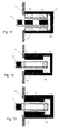
- FIGS 2 to 13 show various examples of the invention applied to components used in an actuator system.
- Figures 2 and 3 show an enclosed actuator system in which the central component comprising the coil 30 moves with respect to the yoke 20 in a direction perpendicular to the plane of the drawing.
- the inner chamber is held in a vacuum and, to reduce outgassing, the coil 30 can be coated with a coating 100 as described above (see Figures 2 and 3).
- the coil 30 in each of these examples is typically glued to its support component using an epoxy-based resin and for this reason, coatings that can be applied and treated using low temperature steps (e.g. less than 200 °C) are preferred.
- the internal parts of the yoke 20 and magnet 10 can also be coated, as shown in Figure 3.
- FIGs 4 to 6 A second type of actuator is shown in Figures 4 to 6.
- the central component is fixed to a chamber wall 40 and the yoke component 20 moves around it in a direction perpendicular to the plane of the drawing.
- Figures 7 and 8 show a similar construction except the presence of two coils 30 and magnets 10 allows relative movement in the left-right direction of the drawing.
- the vacuum is maintained to the right of the chamber wall 40 as it is shown in Figures 4 to 8.
- the coil section 30 is supported by a support 50 in the chamber wall 40 in Figures 4 and 5 whereas the magnet section 10 is supported by the chamber wall 40 in Figures 6, 7 and 8.
- either the coil section 30 can be coated (see Figures 4, 5 and 8) or the magnet section 10 can be coated (see Figures 5, 6, 7 and 8) or both can be coated (see Figures 5 and 8).
- the coating is referenced 100 in each of Figures 2 to 13.
- a third type of actuator is shown in Figures 9 to 13.
- the yoke component 20 is fixed to a chamber wall 40 and the central component moves inside it in a direction perpendicular to the plane of the drawing.
- the yoke component 20 is fixed to a chamber wall 40 and the central component moves inside it in a left-right direction in the plane of the drawing.
- the vacuum is maintained to the left of the chamber wall 40 as it is shown in Figures 9 to 13.
- a yoke section 20, comprising one or more coils 30, is supported by the chamber wall 40 in Figures 9, 10 and 11 whereas a yoke section 20 comprising one or more magnets 10 is shown in Figures 12 and 13.
- either the coil section 30 can be coated (see Figures 10, 11, 12 and 13) or the magnet section 10 can be coated (see Figures 9, 10, 11 and 13) or both can be coated (see Figures 10,11 and 13).
Abstract
A method of preparing components for use in the vacuum chamber of a lithographic
apparatus is disclosed. The method comprises firstly coating the component with a non-metallic,
non-plastics material then treating the coating so as to harden it. The preferred
coating material is a Hydrogen Silsesquioxanc (HSQ) which can be applied using a variety
of methods (spraying, brushing, spinning) and can be treated by either heating or by
irradiation with an electron beam. The resulting components strongly reduce outgassing of
either water or hydrocarbons when subjected to a vacuum environment.
Description
- The present invention relates to a method of preparing components for use in a lithographic projection apparatus comprising:
- a radiation system for supplying a projection beam of radiation;
- a support structure for supporting patterning means, the patterning means serving to pattern the projection beam according to a desired pattern;
- a substrate table for holding a substrate; and
- a projection system for projecting the patterned beam onto a target portion of the substrate.
- The term "patterning means" as here employed should be broadly interpreted as referring to means that can be used to endow an incoming radiation beam with a patterned cross-section, corresponding to a pattern that is to be created in a target portion of the substrate; the term "light valve" can also be used in this context. Generally, the said pattern will correspond to a particular functional layer in a device being created in the target portion, such as an integrated circuit or other device (see below). Examples of such patterning means include:
- A mask. The concept of a mask is well known in lithography, and it includes mask types such as binary, alternating phase-shift, and attenuated phase-shift, as well as various hybrid mask types. Placement of such a mask in the radiation beam causes selective transmission (in the case of a transmissive mask) or reflection (in the case of a reflective mask) of the radiation impinging on the mask, according to the pattern on the mask. In the case of a mask, the support structure will generally be a mask table, which ensures that the mask can be held at a desired position in the incoming radiation beam, and that it can be moved relative to the beam if so desired.
- A programmable mirror array. One example of such a device is a matrix-addressable surface having a viscoelastic control layer and a reflective surface. The basic principle behind such an apparatus is that (for example) addressed areas of the reflective surface reflect incident light as diffracted light, whereas unaddressed areas reflect incident light as undiffracted light. Using an appropriate filter, the said undiffracted light can be filtered out of the reflected beam, leaving only the diffracted light behind; in this manner, the beam becomes patterned according to the addressing pattern of the matrix-addressable surface. An alternative embodiment of a programmable mirror array employs a matrix arrangement of tiny mirrors, each of which can be individually tilted about an axis by applying a suitable localized electric field, or by employing piezoelectric actuation means. Once again, the mirrors are matrix-addressable, such that addressed mirrors will reflect an incoming radiation beam in a different direction to unaddressed mirrors; in this manner, the reflected beam is patterned according to the addressing pattern of the matrix-addressable mirrors. The required matrix addressing can be performed using suitable electronic means. In both of the situations described hereabove, the patterning means can comprise one or more programmable mirror arrays. More information on mirror arrays as here referred to can be gleaned, for example, from United States Patents US 5,296,891 and US 5,523,193, and PCT patent applications WO 98/38597 and WO 98/33096, which are incorporated herein by reference. In the case of a programmable mirror array, the said support structure may be embodied as a frame or table, for example, which may be fixed or movable as required.
- A programmable LCD array. An example of such a construction is given in United States Patent US 5,229,872, which is incorporated herein by reference. As above, the support structure in this case may be embodied as a frame or table, for example, which may be fixed or movable as required.
- Lithographic projection apparatus can be used, for example, in the manufacture of integrated circuits (ICs). In such a case, the patterning means may generate a circuit pattern corresponding to an individual layer of the IC, and this pattern can be imaged onto a target portion (e.g. comprising one or more dies) on a substrate (silicon wafer) that has been coated with a layer of radiation-sensitive material (resist). In general, a single wafer will a whole network of adjacent target portions that are successively irradiated via the projection system, one at a time. In current apparatus, employing patterning by a mask on a mask table, a distinction can be made between two different types of machine. In one type of lithographic projection apparatus, each target portion is irradiated by exposing the entire mask pattern onto the target portion in one go; such an apparatus is commonly referred to as a wafer stepper. In an alternative apparatus ―commonly referred to as a step-and-scan apparatus ― each target portion is irradiated by progressively scanning the mask pattern under the projection beam in a given reference direction (the "scanning" direction) while synchronously scanning the substrate table parallel or anti-parallel to this direction; since, in general, the projection system will have a magnification factor M (generally < 1), the speed V at which the substrate table is scanned will be a factor M times that at which the mask table is scanned. More information with regard to lithographic devices as here described can be gleaned, for example, from US 6,046,792, incorporated herein by reference.
- In a manufacturing process using a lithographic projection apparatus, a pattern (e.g. in a mask) is imaged onto a substrate that is at least partially covered by a layer of radiation-sensitive material (resist). Prior to this imaging step, the substrate may undergo various procedures, such as priming, resist coating and a soft bake. After exposure, the substrate may be subjected to other procedures, such as a post-exposure bake (PEB), development, a hard bake and measurement/inspection of the imaged features. This array of procedures is used as a basis to pattern an individual layer of a device, e.g. an IC. Such a patterned layer may then undergo various processes such as etching, ion-implantation (doping), metallization, oxidation, chemo-mechanical polishing, etc., all intended to finish off an individual layer. If several layers are required, then the whole procedure, or a variant thereof, will have to be repeated for each new layer. Eventually, an array of devices will be present on the substrate (wafer). These devices are then separated from one another by a technique such as dicing or sawing, whence the individual devices can be mounted on a carrier, connected to pins, etc. Further information regarding such processes can be obtained, for example, from the book "Microchip Fabrication: A Practical Guide to Semiconductor Processing", Third Edition, by Peter van Zant, McGraw Hill Publishing Co., 1997, ISBN 0-07-067250-4, incorporated herein by reference.
- For the sake of simplicity, the projection system may hereinafter be referred to as the "lens"; however, this term should be broadly interpreted as encompassing various types of projection system, including refractive optics, reflective optics, and catadioptric systems, for example. The radiation system may also include components operating according to any of these design types for directing, shaping or controlling the projection beam of radiation, and such components may also be referred to below, collectively or singularly, as a "lens". Further, the lithographic apparatus may be of a type having two or more substrate tables (and/or two or more mask tables). In such "multiple stage" devices the additional tables may be used in parallel, or preparatory steps may be carried out on one or more tables while one or more other tables are being used for exposures. Dual stage lithographic apparatus are described, for example, in US 5,969,441 and WO 98/40791, incorporated herein by reference.
- Extreme ultraviolet lithography needs to be carried out in a ultra high vacuum environment because all matter, including atmospheric air, strongly absorbs extreme ultraviolet radiation within a distance ranging from a few millimeters (for gases) to nanometers (for solids). Even for lithography not utilizing extreme ultraviolet radiation, a vacuum or partial vacuum is desirable in order to reduce light absorption. The necessity of a vacuum means that all standard components of the lithographic system, such as stages, optics and sensors are required to operate in a vacuum environment. Each of the components are connected to one another and the external world by a large number of connecting cables and pipes which transport electrical power, electrical signals and cooling water through the system.
- There is therefore a necessity for a vacuum to be maintained in a chamber, which chamber comprises components made from a wide range of materials, ranging from stainless steel to soft plastics. Furthermore, the total surface area of all of the components in the vacuum chamber can be very large due to the fact that many of the components are wires or the like.
- The components in their natural form have a certain surface roughness and surface porosity which allows atoms and molecules to be attached to them under atmospheric conditions during manufacturing. When such components are placed in a vacuum, the atoms and molecules are released thereby reducing the quality of the vacuum and placing an additional burden on the vacuum pump system (e.g. a turbo pump or cryo pump system) that is used to create the vacuum in the vacuum chamber. Furthermore, soft plastics emit plasticizers originating from the bulk of the material. Thus, the components located inside the vacuum chamber can contribute to what is known as "outgassing". Such outgassing results from the fact that the components release molecules into the vacuum from their surfaces. These molecules need to be pumped away by the vacuum pump system in operation. Furthermore, during operation of the lithographic system, the outgassing load on the vacuum pump systems becomes even more onerous due to the contributions from the fresh wafers from the outside world, hydrocarbons emitted from resists before and after radiation and wear and tear of all of the moving parts of the scanner system.
- A similar outgassing problem occurs in lithographic projection apparatus not requiring a vacuum, for example 157 nm machines in which the light transmitting chamber is flushed with Nitrogen. Although no vacuum is present, outgassing still occurs (e.g. by diffusion) and the Nitrogen becomes contaminated which can lead to less reliable exposures.
- It would therefore be desirable to provide a way of reducing the problems associated with outgassing of components in the chamber.
- This and other desires are addressed by the present invention which provides in its first aspect a method of preparing components to reduce outgassing inside a lithographic projection apparatus, said method comprising coating a surface of said components with a non-metallic material.
- The coating of the components with a non-metallic material reduces the contamination originating from the components since any releasable molecules located on the surface of the component are prevented from escaping by the coating layer. Non-metallic materials are used because metallic materials can reduce the efficiency of nearby actuators (e.g. linear motors) and are a source of eddy currents that can damp down actuator signals. Non-plastics materials are preferably used because plastics materials can themselves be a source of outgassing and one aim of invention is to reduce outgassing. Suitable plastics materials (e.g. Teflon) can be used provided they do not themselves introduce an unacceptable outgassing load.
- Preferably, the material is glass or glass-like since such materials are electrical insulators and have been found to be effective in preventing the escape of contaminants from the surface of components. Glass or glass-like coatings can be used to protect polymer components from degradation from direct EUV illumination or electron induced degradation. Without the coating, these two mechanisms can cause a large amount of outgassing. Thus, such coatings are useful in preventing outgassing from components such as cables and connectors. Preferably, the coating is a silica glass although phospate glass and other types of glass can be used if need be.
- Hydrogen silsesquioxane (HSQ) is a particularly preferred precursor material for the coating. It can be applied by spraying, brushing or spinning as a liquid composition and can then be treated so that it becomes hard and glass-like, that is to say, electrically insulating, amorphous and without showing any outgassing of water and/or hydrocarbons by itself after application. Instead of HSQ, a silsesquioxane (SQ) precursor material with one or more hydrocarbon groups attached can be used. Such coatings formed using such precursors are so-called "hybrid coatings", which have partly organic and partly inorganic features.
- Other application techniques, for example PVD techniques such as sputtering or evaporation or CVD techniques can also be used for applying coatings onto the components.
- The treating can include thermal treating or irradiation by electrons. When HSQ is used, the cage-like structure of the liquid composition is broken down into a solid amorphous quartz-like structure that is believed to be particularly effective at preventing outgassing.
- In a second aspect, the invention provides a component for use in a lithographic projection apparatus, said component having a surface coated with 30nm or more of a glass or glass-like material.
- According to a third aspect of the invention, there is provided a lithographic projection apparatus comprising:
- a radiation system for providing a projection beam of radiation;
- a support structure for supporting patterning means, the patterning means serving to pattern the projection beam according to a desired pattern;
- a substrate table for holding a substrate;
- a projection system for projecting the patterned beam onto a target portion of the substrate, characterized in that said apparatus comprises at least one component prepared according the first aspect of the invention or a component according to the second aspect of the invention.
-
- According to a fourth aspect of the invention there is provided a device manufacturing method comprising the steps of:
- providing a substrate that is at least partially covered by a layer of radiation-sensitive material;
- providing a projection beam of radiation using a radiation system;
- using patterning means to endow the projection beam with a pattern in its cross-section;
- projecting the patterned beam of radiation onto a target portion of the layer of radiation-sensitive material,
- Although specific reference may be made in this text to the use of the apparatus according to the invention in the manufacture of ICs, it should be explicitly understood that such an apparatus has many other possible applications. For example, it may be employed in the manufacture of integrated optical systems, guidance and detection patterns for magnetic domain memories, liquid-crystal display panels, thin-film magnetic heads, etc. The skilled artisan will appreciate that, in the context of such alternative applications, any use of the terms "reticle", "wafer" or "die" in this text should be considered as being replaced by the more general terms "mask", "substrate" and "target portion", respectively.
- In the present document, the terms "radiation" and "beam" are used to encompass all types of electromagnetic radiation, including ultraviolet radiation (e.g. with a wavelength of 365, 248, 193, 157 or 126 nm) and EUV (extreme ultra-violet radiation, e.g. having a wavelength in the range 5-20 nm), as well as particle beams, such as ion beams or electron beams.
- Embodiments of the invention will now be described, by way of example only, with reference to the accompanying schematic drawings in which:
- Figure 1 depicts a lithographic projection apparatus according to an embodiment of the invention; and
- Figures 2 to 13 show alternative coating arrangements for the case when the invention is applied to an actuator system in said lithographic projection apparatus.
-
- Figure 1 schematically depicts a lithographic projection apparatus comprising the vacuum chamber using one or more components prepared according to any of the embodiments of the present invention. The apparatus comprises:
- a radiation system Ex, IL, for supplying a projection beam PB of radiation (e.g. EUV radiation), which in this particular case also comprises a radiation source LA;
- a first object table (mask table) MT provided with a mask holder for holding a mask MA (e.g. a reticle), and connected to first positioning means for accurately positioning the mask with respect to item PL;
- a second object table (substrate table) WT provided with a substrate holder for holding a substrate W (e.g. a resist-coated silicon wafer), and connected to second positioning means for accurately positioning the substrate with respect to item PL;
- a projection system ("lens") PL (e.g. mirror group) for imaging an irradiated portion of the mask MA onto a target portion C (e.g. comprising one or more dies) of the substrate W.
- As here depicted, the apparatus is of a reflective type (e.g. has a reflective mask). However, in general, it may also be of a transmissive type, for example (e.g. with a transmissive mask). Alternatively, the apparatus may employ another kind of patterning means, such as a programmable mirror array of a type as referred to above.
- The source LA (e.g. a laser-produced or discharge plasma source) produces a beam of radiation. This beam is fed into an illumination system (illuminator) IL, either directly or after having traversed conditioning means, such as a beam expander Ex, for example. The illuminator IL may comprise adjusting means AM for setting the outer and/or inner radial extent (commonly referred to as σ-outer and σ-inner, respectively) of the intensity distribution in the beam. In addition, it will generally comprise various other components, such as an integrator IN and a condenser CO. In this way, the beam PB impinging on the mask MA has a desired uniformity and intensity distribution in its cross-section.
- It should be noted with regard to Figure 1 that the source LA may be within the housing of the lithographic projection apparatus (as is often the case when the source LA is a mercury lamp, for example), but that it may also be remote from the lithographic projection apparatus, the radiation beam which it produces being led into the apparatus (e.g. with the aid of suitable directing mirrors); this latter scenario is often the case when the source LA is an excimer laser. The current invention and Claims encompass both of these scenarios.
- The beam PB subsequently intercepts the mask MA, which is held on a mask table MT. Having been selectively reflected by the mask MA, the beam PB passes through the lens PL, which focuses the beam PB onto a target portion C of the substrate W. With the aid of the second positioning means (and interferometric measuring means IF), the substrate table WT can be moved accurately, e.g. so as to position different target portions C in the path of the beam PB. Similarly, the first positioning means can be used to accurately position the mask MA with respect to the path of the beam PB, e.g. after mechanical retrieval of the mask MA from a mask library, or during a scan. In general, movement of the object tables MT, WT will be realized with the aid of a long-stroke module (course positioning) and a short-stroke module (fine positioning), which are not explicitly depicted in Figure 1. However, in the case of a wafer stepper (as opposed to a step-and-scan apparatus) the mask table MT may just be connected to a short stroke actuator, or may be fixed.
- The depicted apparatus can be used in two different modes:
- 1. In step mode, the mask table MT is kept essentially stationary, and an entire mask image is projected in one go (i.e. a single "flash") onto a target portion C. The substrate table WT is then shifted in the x and/or y directions so that a different target portion C can be irradiated by the beam PB;
- 2. In scan mode, essentially the same scenario applies, except that a given target portion C is not exposed in a single "flash". Instead, the mask table MT is movable in a given direction (the so-called "scan direction", e.g. the y direction) with a speed v, so that the projection beam PB is caused to scan over a mask image; concurrently, the substrate table WT is simultaneously moved in the same or opposite direction at a speed V= Mv, in which M is the magnification of the lens PL (typically, M= 1/4 or 1/5). In this manner, a relatively large target portion C can be exposed, without having to compromise on resolution.
-
- In a practical embodiment of the lithographic projection apparatus, the spaces through which the EUV radiation beam travels will be evacuated by means of a vacuum pumping system. The chamber in which the vacuum is to be maintained will typically comprise many components made of a variety of materials. For example, wires intended for transmitting electrical currents will often traverse the vacuum chamber and such wires may be manufactured from an inner metal core with a plastics material surround. Soft plastics materials typically used for wires emit molecules over time contributing to the outgassing burden that the vacuum pumping system needs to remove. Also, the coils and magnets of the actuator system used to position the various tables can cause outgassing. The present invention thus comprises a method of preparing components before they are placed in the vacuum environment and after they have been manufactured. The invention can also be used in other situations where outgassing reduction is desirable, for example to coat components used in the Nitrogen flushed chamber of a 157nm wavelength lithographic apparatus. The preferred method has two stages:-
- 1. Coating the component with a non-metallic liquid composition; and
- 2. Treating the coated component to harden the coating layer and to make it effective at preventing outgassing.
-
- The invention is particularly applicable to coat the coils of a linear actuator used for moving the tables of the lithographic apparatus. The coating is preferable to the chamber wall (20) disclosed in US 6,271,606 which, due to its stainless steel material, is susceptible to eddy currents and results in a loss in efficiency of the linear motor. Furthermore, the present invention has an advantage over the metal film disclosed in EP 1,233,501 which also suffers from the problem of eddy currents and is not very efficient at preventing outgassing. Metal coatings are also difficult to apply because it is necessary to carefully control the deposition process to control the crystal structure and avoid pinholes.
- Any non-metallic material can be used. The material is preferably a non-plastics material. Glass or glass-like materials are preferred because they have been found to be particularly effective. Such materials include diamond and a family of materials known under the generic name Silsesquioxane (SQ). These chemicals have the general basic formula RSiO1.5 where substituent R is an atom or molecule that can bond with silicon, for example a polymerizable organic group such as hydrido, glycidyl, methyl, vinyl, propyl, methacrylate, cyclohexenyl, cyclohexenyl epoxide etc. The molecules are usually represented in a cubic structure with a silicon atom at each cube comer. This cubic structure has the basic formula (RSi)8O12 with each silicon atom being bound to three oxygen atoms and the substituent R.
- Hydrogen Silsesquioxane (HSQ) has been used in the past as a resist material for electron beam patterning applications but its use as an outgassing prevention material has not heretofore been suggested. It is particularly suitable because it can be applied to the component using a variety of convenient methods. For example, it can simply be sprayed or brushed onto the component so as to cover all of the potential outgassing surfaces and to clog all outgassing micro-pores with a sufficiently thick layer of material. More preferably, the liquid composition can be applied using a spinning process, for example using a Karl Suss spinner having a lid. Application of the material not only fills in surface micro-pores but also helps to planerise the material by reducing surface roughness. Once treated, the material coating strongly reduces the outgassing of water and hydrocarbons that would otherwise occur from the porous surfaces and plastic surfaces of the components. Any SQ precursor may be used, preferably with one or more hydrocarbon groups attached.
- The method may be applied to any components, so long as it does not hinder the functioning of the component itself. For example, printed circuit boards, electric cables, support surfaces, actuators and the like may all be coated.
- The preferred HSQ material for the coating is available commercially, for example from Dow-Corning under the reference FOX-12. This material initially shows liquid-like properties which enables the coating of the outgassing surfaces and parts, covering the surfaces and filling the micro-pores.
- The coating layer may be applied to any desired thickness, but a thickness of at least 30nm is preferred to ensure good outgassing prevention capability. Thicknesses of between about 100nm and of the order of 1 micron will allow the component to retain some of its inherent flexibility whereas great thicknesses will cause a rigid coating to be prepared on the component. Hybrid coatings may be thicker whilst still retaining flexibility.
- Two methods may be used to treat the coated component so as to harden the coating layer and permanently reduce the outgassing capability of the component.
- The first method is a thermal treatment method whereby the surface of the component is heated up. This changes the chemical structure of the coating layer so as to harden it. It can be achieved by placing the component in an oven at 100 to 500°C, more preferably 200 to 400°C to carry out the desired effect.
- The second method is to irradiate the surface of the component using a wavelength of a radiation that will cause the desired transformation. Infrared radiation may be used to cause heating of the surface and such treatment works in a similar way to the thermal treatment. Alternatively, an electron beam may be used, particularly when a HSQ material is used for the coating material, which exposes the coating material, changing its chemical structure from a cage-like structure to an amorphous quartz-like structure.
- The change in structure leaves a hard surface on the component that strongly reduces outgassing even when the component is placed in a vacuum.
- Once the coating and treating steps have been carried out, the component is available for use in the lithographic projection apparatus. If desired, the coating-developing cycle can be repeated one or more further times to reduce the outgassing potential of the components still further. The components may then be further processed if necessary or be used straight away in the lithographic apparatus.
- Polymer coatings are good at adhering to the component but are less successful at reducing outgassing. Thus, a two or more stage process in which a polymer coating is initially used and is followed by a glass-like top coating allows one to benefit from the advantages of both types of coating whilst maintaining excellent outgassing reduction.
- It is to be understood that the term "vacuum" is used in this description to refer to the degree of vacuum commonly found in lithographic projection devices. It is not to be strictly interpreted as requiring a pure vacuum. A partial vacuum will suffice.
- Figures 2 to 13 show various examples of the invention applied to components used in an actuator system.
- Figures 2 and 3 show an enclosed actuator system in which the central component comprising the
coil 30 moves with respect to theyoke 20 in a direction perpendicular to the plane of the drawing. The inner chamber is held in a vacuum and, to reduce outgassing, thecoil 30 can be coated with acoating 100 as described above (see Figures 2 and 3). Thecoil 30 in each of these examples is typically glued to its support component using an epoxy-based resin and for this reason, coatings that can be applied and treated using low temperature steps (e.g. less than 200 °C) are preferred. The internal parts of theyoke 20 andmagnet 10 can also be coated, as shown in Figure 3. - A second type of actuator is shown in Figures 4 to 6. Here, the central component is fixed to a
chamber wall 40 and theyoke component 20 moves around it in a direction perpendicular to the plane of the drawing. Figures 7 and 8 show a similar construction except the presence of twocoils 30 andmagnets 10 allows relative movement in the left-right direction of the drawing. The vacuum is maintained to the right of thechamber wall 40 as it is shown in Figures 4 to 8. Thecoil section 30 is supported by asupport 50 in thechamber wall 40 in Figures 4 and 5 whereas themagnet section 10 is supported by thechamber wall 40 in Figures 6, 7 and 8. In each case, either thecoil section 30 can be coated (see Figures 4, 5 and 8) or themagnet section 10 can be coated (see Figures 5, 6, 7 and 8) or both can be coated (see Figures 5 and 8). The coating is referenced 100 in each of Figures 2 to 13. - A third type of actuator is shown in Figures 9 to 13. In Figures 10, 12 and 13, the
yoke component 20 is fixed to achamber wall 40 and the central component moves inside it in a direction perpendicular to the plane of the drawing. In Figures 9 and 11, theyoke component 20 is fixed to achamber wall 40 and the central component moves inside it in a left-right direction in the plane of the drawing. In each case, the vacuum is maintained to the left of thechamber wall 40 as it is shown in Figures 9 to 13. Ayoke section 20, comprising one ormore coils 30, is supported by thechamber wall 40 in Figures 9, 10 and 11 whereas ayoke section 20 comprising one ormore magnets 10 is shown in Figures 12 and 13. In each case, either thecoil section 30 can be coated (see Figures 10, 11, 12 and 13) or themagnet section 10 can be coated (see Figures 9, 10, 11 and 13) or both can be coated (see Figures 10,11 and 13). - Whilst specific embodiments of the invention have been described above, it will be appreciated that the invention may be practiced otherwise than as described. The description is not intended to limit the invention.
Claims (21)
- A method of preparing a component to reduce outgassing inside a lithographic projection apparatus, said method comprising:coating a surface of said component with a non-metallic material.
- A method according to claim 1, wherein said material is a non-plastics material.
- A method according to claim 1 or 2, wherein said material is glass or glass-like.
- A method according to claim 3, wherein said material is a silica glass.
- A method according to claim 3, wherein said material is hydrogen silsesquioxane (HSQ) or a silsesquioxane precursor with one or more hydrocarbon groups attached.
- A method according to nay one of claims 1 to 5, wherein said coating step comprises:applying a fluid composition of said material to a surface of said component.
- A method according to claim 6, wherein said coating step comprises:spraying said fluid composition of said material onto a surface of said component.
- A method according to claim 6, wherein said coating step comprises:brushing said fluid composition of said material onto a surface of said component.
- A method according to claim 6, wherein said coating step comprises:spinning said liquid composition of said material onto a surface of said component.
- A method according to any one of claims 6 to 9, further comprising:treating said coated component to harden the coating.
- A method according to claim 10, wherein said treated coating is a hard amorphous layer of electrically insulating material.
- A method according to claim 10 or 11, wherein said treating step comprises:heating the coated surface.
- A method according to claim 12, wherein said heating is carried out at 100°C to 500°C for at least one minute.
- A method according to claim 10 or 11, wherein said treating step comprises:irradiating the coated surface with an electron beam.
- A method according to claim 10 or 11, wherein said treating step comprises:irradiating the coated surface using a wavelength of radiation which will cause the hardening of the coating.
- A method according to claim 15, wherein the radiation is infrared radiation.
- A method according to any one of the preceding claims, wherein said material is coated to a depth of 30nm or more.
- A method according to any one of claims 1 to 17, wherein said component is an actuator comprising at least one coil and at least one magnet.
- A component for use in a lithographic projection apparatus, said component having a surface coated with 30nm or more of a glass or glass-like material.
- A lithographic projection apparatus comprising:characterised in that said apparatus comprises at least one component prepared according to any one of claims 1 to 19 or according to claim 20.a radiation system for providing a projection beam of radiation;a support structure for supporting patterning means, the patterning means serving to pattern the projection beam according to a desired pattern;a substrate table for holding a substrate;a projection system for projecting the patterned beam onto a target portion of the substrate,
- A device manufacturing method comprising the steps of:characterised by using a component prepared according to any one of claims 1 to 19 or according to claim 20.providing a substrate that is at least partially covered by a layer of radiation-sensitive material;providing a projection beam of radiation using a radiation system;using patterning means to endow the projection beam with a pattern in its cross-section;projecting the patterned beam of radiation onto a target portion of the layer of radiation-sensitive material,
Priority Applications (9)
| Application Number | Priority Date | Filing Date | Title |
|---|---|---|---|
| EP03252894A EP1475668A1 (en) | 2003-05-09 | 2003-05-09 | Method of preparing components for a lithographic apparatus |
| SG200402413A SG116541A1 (en) | 2003-05-09 | 2004-05-06 | A method of preparing components, prepared component, lithographic apparatus and device manufacturing method. |
| JP2004166401A JP4178131B2 (en) | 2003-05-09 | 2004-05-07 | Component preparation processing method, preparation processed component, lithographic apparatus, and device manufacturing method |
| DE602004020012T DE602004020012D1 (en) | 2003-05-09 | 2004-05-07 | Process for the preparation of a lithographic apparatus |
| US10/840,508 US8077287B2 (en) | 2003-05-09 | 2004-05-07 | Method of preparing components, prepared component, lithographic apparatus and device manufacturing method |
| KR1020040032143A KR100749950B1 (en) | 2003-05-09 | 2004-05-07 | A method of preparing components, prepared component, lithographic apparatus and device manufacturing method |
| EP04252674A EP1475671B1 (en) | 2003-05-09 | 2004-05-07 | Method of making a lithographic apparatus |
| TW093112968A TW200502712A (en) | 2003-05-09 | 2004-05-07 | A method of preparing components, prepared component, lithographic apparatus and device manufacturing method |
| CNB2004100550277A CN100495211C (en) | 2003-05-09 | 2004-05-08 | Method of preparing components, prepared component, lithographic apparatus and device manufacturing method |
Applications Claiming Priority (1)
| Application Number | Priority Date | Filing Date | Title |
|---|---|---|---|
| EP03252894A EP1475668A1 (en) | 2003-05-09 | 2003-05-09 | Method of preparing components for a lithographic apparatus |
Publications (1)
| Publication Number | Publication Date |
|---|---|
| EP1475668A1 true EP1475668A1 (en) | 2004-11-10 |
Family
ID=32981964
Family Applications (2)
| Application Number | Title | Priority Date | Filing Date |
|---|---|---|---|
| EP03252894A Withdrawn EP1475668A1 (en) | 2003-05-09 | 2003-05-09 | Method of preparing components for a lithographic apparatus |
| EP04252674A Expired - Fee Related EP1475671B1 (en) | 2003-05-09 | 2004-05-07 | Method of making a lithographic apparatus |
Family Applications After (1)
| Application Number | Title | Priority Date | Filing Date |
|---|---|---|---|
| EP04252674A Expired - Fee Related EP1475671B1 (en) | 2003-05-09 | 2004-05-07 | Method of making a lithographic apparatus |
Country Status (8)
| Country | Link |
|---|---|
| US (1) | US8077287B2 (en) |
| EP (2) | EP1475668A1 (en) |
| JP (1) | JP4178131B2 (en) |
| KR (1) | KR100749950B1 (en) |
| CN (1) | CN100495211C (en) |
| DE (1) | DE602004020012D1 (en) |
| SG (1) | SG116541A1 (en) |
| TW (1) | TW200502712A (en) |
Cited By (1)
| Publication number | Priority date | Publication date | Assignee | Title |
|---|---|---|---|---|
| EP1542076A2 (en) * | 2003-12-08 | 2005-06-15 | ASML Netherlands B.V. | Lithographic apparatus and device manufacturing method |
Families Citing this family (8)
| Publication number | Priority date | Publication date | Assignee | Title |
|---|---|---|---|---|
| FR2903823B1 (en) * | 2006-07-12 | 2008-09-05 | Messier Dowty Sa | ELECTROMAGNETIC MACHINE ACTIVE ELEMENT, METHOD OF MANUFACTURING SUCH ACTIVE ELEMENT, AND ELECTROMAGNETIC MACHINE COMPRISING SUCH ACTIVE ELEMENT. |
| KR101437583B1 (en) * | 2007-07-03 | 2014-09-12 | 삼성전자주식회사 | Lithography apparatus and lithography method |
| NL1036543A1 (en) * | 2008-02-20 | 2009-08-24 | Asml Netherlands Bv | Lithographic apparatus including a magnet, method for the protection of a magnet in a lithographic apparatus and device manufacturing method. |
| CN101625522B (en) * | 2008-07-09 | 2012-03-21 | 中国科学院微电子研究所 | Method for preparing dense pattern on thick negative high resolution electron beam resist HSQ |
| DE102009005340A1 (en) * | 2009-01-16 | 2010-07-22 | Carl Zeiss Smt Ag | EUV lithography system and cables for it |
| DE102009008209A1 (en) * | 2009-02-10 | 2010-08-19 | Carl Zeiss Smt Ag | Actuator with at least one magnet for a projection exposure apparatus and projection exposure apparatus with a magnet and manufacturing method thereof |
| TWI422985B (en) * | 2009-03-12 | 2014-01-11 | Raydium Semiconductor Corp | Nano-lithography system and nano-lithography method |
| CN102681335B (en) * | 2011-03-15 | 2013-08-07 | 中国科学院微电子研究所 | Method for preparing phase type diffraction optical element according to wet etching |
Citations (7)
| Publication number | Priority date | Publication date | Assignee | Title |
|---|---|---|---|---|
| WO2000013223A1 (en) * | 1998-08-31 | 2000-03-09 | Alliedsignal Inc. | Nanoporous dielectric thin films |
| JP2001153140A (en) * | 1999-11-26 | 2001-06-08 | Fujitsu Ltd | Gas bearing |
| US6296806B1 (en) * | 1997-02-28 | 2001-10-02 | Extraction Systems, Inc. | Protection of semiconductor fabrication and similar sensitive processes |
| US20020011182A1 (en) * | 1996-06-24 | 2002-01-31 | Masayuki Matsuda | Coating liquid for forming transparent coating, substrate with transparent coating and use thereof |
| EP1204002A2 (en) * | 2000-11-01 | 2002-05-08 | TRW Inc. | EUV lithography system with thin-film coating for protection from laser-produced plasma |
| EP1233501A2 (en) * | 2001-02-16 | 2002-08-21 | Canon Kabushiki Kaisha | Linear motor, stage apparatus, exposure apparatus and device manufacturing method |
| US20020145808A1 (en) * | 2001-02-24 | 2002-10-10 | Carl Zeiss Semiconductor Manufacturing Technologies Ag | Optical beam guidance system and method for preventing contamination of optical components contained therein |
Family Cites Families (24)
| Publication number | Priority date | Publication date | Assignee | Title |
|---|---|---|---|---|
| US4040874A (en) * | 1975-08-04 | 1977-08-09 | General Electric Company | Semiconductor element having a polymeric protective coating and glass coating overlay |
| JPH04239130A (en) * | 1991-01-11 | 1992-08-27 | Kawasaki Steel Corp | Plasma processor and processing method |
| JPH0639959A (en) | 1992-02-03 | 1994-02-15 | Showa Denko Kk | Method for decorating surface of cement-cured product |
| JP3167044B2 (en) * | 1992-02-13 | 2001-05-14 | 日本トムソン株式会社 | DC linear motor and linear motion unit having the same |
| JP3174417B2 (en) * | 1992-12-11 | 2001-06-11 | ダウ・コ−ニング・コ−ポレ−ション | Method for forming silicon oxide film |
| JPH06267486A (en) | 1993-03-17 | 1994-09-22 | Toshiba Corp | Charged electron beam device |
| US5439849A (en) * | 1994-02-02 | 1995-08-08 | At&T Corp. | Encapsulation techniques which include forming a thin glass layer onto a polymer layer |
| US5456952A (en) * | 1994-05-17 | 1995-10-10 | Lsi Logic Corporation | Process of curing hydrogen silsesquioxane coating to form silicon oxide layer |
| US5609925A (en) * | 1995-12-04 | 1997-03-11 | Dow Corning Corporation | Curing hydrogen silsesquioxane resin with an electron beam |
| KR100238252B1 (en) * | 1996-09-13 | 2000-01-15 | 윤종용 | Method for curing sog layer |
| KR100469142B1 (en) * | 1997-12-10 | 2005-06-21 | 주식회사 하이닉스반도체 | Metal contamination prevention method of semiconductor device |
| US5942801A (en) * | 1997-12-18 | 1999-08-24 | Advanced Micro Devices, Inc. | Borderless vias with HSQ gap filled metal patterns having high etching resistance |
| US6031598A (en) * | 1998-09-25 | 2000-02-29 | Euv Llc | Extreme ultraviolet lithography machine |
| US6114781A (en) * | 1999-02-26 | 2000-09-05 | Nikon Corporation | Cooling system for a linear or planar motor |
| US6271606B1 (en) * | 1999-12-23 | 2001-08-07 | Nikon Corporation | Driving motors attached to a stage that are magnetically coupled through a chamber |
| JP4474020B2 (en) * | 2000-06-23 | 2010-06-02 | キヤノン株式会社 | Moving apparatus and exposure apparatus |
| JP4110504B2 (en) * | 2001-03-13 | 2008-07-02 | 株式会社安川電機 | Vacuum motor |
| US6773950B2 (en) * | 2001-05-25 | 2004-08-10 | Cornell Research Foundation, Inc. | Method of forming dual exposure glass layer structures |
| KR20030017753A (en) * | 2001-08-22 | 2003-03-04 | 삼성전자주식회사 | Chamber having a double inner sheild ring |
| US7282821B2 (en) * | 2002-01-28 | 2007-10-16 | Canon Kabushiki Kaisha | Linear motor, stage apparatus, exposure apparatus, and device manufacturing apparatus |
| JP3809381B2 (en) * | 2002-01-28 | 2006-08-16 | キヤノン株式会社 | Linear motor, stage apparatus, exposure apparatus, and device manufacturing method |
| US7579681B2 (en) * | 2002-06-11 | 2009-08-25 | Micron Technology, Inc. | Super high density module with integrated wafer level packages |
| US7183674B2 (en) * | 2003-11-06 | 2007-02-27 | Carl Zeiss Smt Ag | Hermetically sealed elements of an actuator |
| US7184123B2 (en) * | 2004-03-24 | 2007-02-27 | Asml Netherlands B.V. | Lithographic optical system |
-
2003
- 2003-05-09 EP EP03252894A patent/EP1475668A1/en not_active Withdrawn
-
2004
- 2004-05-06 SG SG200402413A patent/SG116541A1/en unknown
- 2004-05-07 JP JP2004166401A patent/JP4178131B2/en not_active Expired - Fee Related
- 2004-05-07 DE DE602004020012T patent/DE602004020012D1/en not_active Expired - Fee Related
- 2004-05-07 US US10/840,508 patent/US8077287B2/en not_active Expired - Fee Related
- 2004-05-07 TW TW093112968A patent/TW200502712A/en unknown
- 2004-05-07 KR KR1020040032143A patent/KR100749950B1/en not_active IP Right Cessation
- 2004-05-07 EP EP04252674A patent/EP1475671B1/en not_active Expired - Fee Related
- 2004-05-08 CN CNB2004100550277A patent/CN100495211C/en not_active Expired - Fee Related
Patent Citations (7)
| Publication number | Priority date | Publication date | Assignee | Title |
|---|---|---|---|---|
| US20020011182A1 (en) * | 1996-06-24 | 2002-01-31 | Masayuki Matsuda | Coating liquid for forming transparent coating, substrate with transparent coating and use thereof |
| US6296806B1 (en) * | 1997-02-28 | 2001-10-02 | Extraction Systems, Inc. | Protection of semiconductor fabrication and similar sensitive processes |
| WO2000013223A1 (en) * | 1998-08-31 | 2000-03-09 | Alliedsignal Inc. | Nanoporous dielectric thin films |
| JP2001153140A (en) * | 1999-11-26 | 2001-06-08 | Fujitsu Ltd | Gas bearing |
| EP1204002A2 (en) * | 2000-11-01 | 2002-05-08 | TRW Inc. | EUV lithography system with thin-film coating for protection from laser-produced plasma |
| EP1233501A2 (en) * | 2001-02-16 | 2002-08-21 | Canon Kabushiki Kaisha | Linear motor, stage apparatus, exposure apparatus and device manufacturing method |
| US20020145808A1 (en) * | 2001-02-24 | 2002-10-10 | Carl Zeiss Semiconductor Manufacturing Technologies Ag | Optical beam guidance system and method for preventing contamination of optical components contained therein |
Non-Patent Citations (1)
| Title |
|---|
| PATENT ABSTRACTS OF JAPAN vol. 2000, no. 23 10 February 2001 (2001-02-10) * |
Cited By (1)
| Publication number | Priority date | Publication date | Assignee | Title |
|---|---|---|---|---|
| EP1542076A2 (en) * | 2003-12-08 | 2005-06-15 | ASML Netherlands B.V. | Lithographic apparatus and device manufacturing method |
Also Published As
| Publication number | Publication date |
|---|---|
| KR20040096772A (en) | 2004-11-17 |
| US20050008978A1 (en) | 2005-01-13 |
| CN1573570A (en) | 2005-02-02 |
| DE602004020012D1 (en) | 2009-04-30 |
| EP1475671B1 (en) | 2009-03-18 |
| EP1475671A1 (en) | 2004-11-10 |
| JP2004343129A (en) | 2004-12-02 |
| KR100749950B1 (en) | 2007-08-16 |
| JP4178131B2 (en) | 2008-11-12 |
| CN100495211C (en) | 2009-06-03 |
| US8077287B2 (en) | 2011-12-13 |
| TW200502712A (en) | 2005-01-16 |
| SG116541A1 (en) | 2005-11-28 |
Similar Documents
| Publication | Publication Date | Title |
|---|---|---|
| KR100713190B1 (en) | Method for coating a substrate for EUV lithography and substrate with photoresist layer | |
| US7106832B2 (en) | Apparatus including a radiation source, a filter system for filtering particles out of radiation emitted by the source, and a processing system for processing the radiation, a lithographic apparatus including such an apparatus, and a method of filtering particles out of radiation emitting and propagating from a radiation source | |
| US7541699B2 (en) | Magnet assembly, linear actuator, planar motor and lithographic apparatus | |
| US7675201B2 (en) | Lithographic apparatus with planar motor driven support | |
| US20050157283A1 (en) | Optical element with a self-assembled monolayer, lithographic projection apparatus including such an optical element, and device manufacturing method | |
| EP1429189B1 (en) | Lithographic apparatus and device manufacturing method | |
| US7274431B2 (en) | Lithographic projection apparatus and device manufacturing method | |
| EP1480078A1 (en) | Method for coating a substrate for EUV lithography and substrate with photoresist layer | |
| EP1475671B1 (en) | Method of making a lithographic apparatus | |
| JP2006339634A (en) | Lithography apparatus, and method of manufacturing device | |
| US7224429B2 (en) | Lithographic apparatus, device manufacturing method and positioning system | |
| US20090268190A1 (en) | Lithographic apparatus and device manufacturing method | |
| CN107850852B (en) | Movable support and lithographic apparatus | |
| US20100103390A1 (en) | Lithographic apparatus and device manufacturing method | |
| US7592760B2 (en) | Lithographic apparatus and device manufacturing method | |
| EP1385051A1 (en) | EUV lithographic projection apparatus comprising an optical element with a self-assembled monolayer, optical element with a self-assembled monolayer, method of applying a self-assembled monolayer and device manufacturing method | |
| US7978307B2 (en) | Gas bearing, and lithographic apparatus provided with such a bearing | |
| US7256863B2 (en) | Sealing assembly, a lithographic projection apparatus, and a device manufacturing method | |
| EP1596421A2 (en) | Lithographic apparatus and device manufacturing method | |
| EP1248148A1 (en) | Lithographic patterning means with protective layer | |
| EP1333329A1 (en) | Lithographic apparatus and device manufacturing method |
Legal Events
| Date | Code | Title | Description |
|---|---|---|---|
| PUAI | Public reference made under article 153(3) epc to a published international application that has entered the european phase |
Free format text: ORIGINAL CODE: 0009012 |
|
| AK | Designated contracting states |
Kind code of ref document: A1 Designated state(s): AT BE BG CH CY CZ DE DK EE ES FI FR GB GR HU IE IT LI LU MC NL PT RO SE SI SK TR |
|
| AX | Request for extension of the european patent |
Extension state: AL LT LV MK |
|
| STAA | Information on the status of an ep patent application or granted ep patent |
Free format text: STATUS: THE APPLICATION IS DEEMED TO BE WITHDRAWN |
|
| 18D | Application deemed to be withdrawn |
Effective date: 20040910 |