EP3203511A1 - Hybrid electronic device protected against moisture and method for protecting a hybrid electronic device against moisture - Google Patents
Hybrid electronic device protected against moisture and method for protecting a hybrid electronic device against moisture Download PDFInfo
- Publication number
- EP3203511A1 EP3203511A1 EP17153660.0A EP17153660A EP3203511A1 EP 3203511 A1 EP3203511 A1 EP 3203511A1 EP 17153660 A EP17153660 A EP 17153660A EP 3203511 A1 EP3203511 A1 EP 3203511A1
- Authority
- EP
- European Patent Office
- Prior art keywords
- layer
- mineral material
- interconnections
- deposition
- nanometers
- Prior art date
- Legal status (The legal status is an assumption and is not a legal conclusion. Google has not performed a legal analysis and makes no representation as to the accuracy of the status listed.)
- Granted
Links
Images

Classifications
-
- H—ELECTRICITY
- H01—ELECTRIC ELEMENTS
- H01L—SEMICONDUCTOR DEVICES NOT COVERED BY CLASS H10
- H01L21/00—Processes or apparatus adapted for the manufacture or treatment of semiconductor or solid state devices or of parts thereof
- H01L21/02—Manufacture or treatment of semiconductor devices or of parts thereof
- H01L21/04—Manufacture or treatment of semiconductor devices or of parts thereof the devices having at least one potential-jump barrier or surface barrier, e.g. PN junction, depletion layer or carrier concentration layer
- H01L21/50—Assembly of semiconductor devices using processes or apparatus not provided for in a single one of the subgroups H01L21/06 - H01L21/326, e.g. sealing of a cap to a base of a container
- H01L21/56—Encapsulations, e.g. encapsulation layers, coatings
- H01L21/563—Encapsulation of active face of flip-chip device, e.g. underfilling or underencapsulation of flip-chip, encapsulation preform on chip or mounting substrate
-
- H—ELECTRICITY
- H01—ELECTRIC ELEMENTS
- H01L—SEMICONDUCTOR DEVICES NOT COVERED BY CLASS H10
- H01L23/00—Details of semiconductor or other solid state devices
- H01L23/16—Fillings or auxiliary members in containers or encapsulations, e.g. centering rings
- H01L23/18—Fillings characterised by the material, its physical or chemical properties, or its arrangement within the complete device
- H01L23/26—Fillings characterised by the material, its physical or chemical properties, or its arrangement within the complete device including materials for absorbing or reacting with moisture or other undesired substances, e.g. getters
-
- H—ELECTRICITY
- H01—ELECTRIC ELEMENTS
- H01L—SEMICONDUCTOR DEVICES NOT COVERED BY CLASS H10
- H01L23/00—Details of semiconductor or other solid state devices
- H01L23/28—Encapsulations, e.g. encapsulating layers, coatings, e.g. for protection
- H01L23/29—Encapsulations, e.g. encapsulating layers, coatings, e.g. for protection characterised by the material, e.g. carbon
- H01L23/291—Oxides or nitrides or carbides, e.g. ceramics, glass
-
- H—ELECTRICITY
- H01—ELECTRIC ELEMENTS
- H01L—SEMICONDUCTOR DEVICES NOT COVERED BY CLASS H10
- H01L23/00—Details of semiconductor or other solid state devices
- H01L23/28—Encapsulations, e.g. encapsulating layers, coatings, e.g. for protection
- H01L23/31—Encapsulations, e.g. encapsulating layers, coatings, e.g. for protection characterised by the arrangement or shape
- H01L23/3157—Partial encapsulation or coating
- H01L23/3171—Partial encapsulation or coating the coating being directly applied to the semiconductor body, e.g. passivation layer
-
- H—ELECTRICITY
- H01—ELECTRIC ELEMENTS
- H01L—SEMICONDUCTOR DEVICES NOT COVERED BY CLASS H10
- H01L23/00—Details of semiconductor or other solid state devices
- H01L23/28—Encapsulations, e.g. encapsulating layers, coatings, e.g. for protection
- H01L23/31—Encapsulations, e.g. encapsulating layers, coatings, e.g. for protection characterised by the arrangement or shape
- H01L23/3157—Partial encapsulation or coating
- H01L23/3178—Coating or filling in grooves made in the semiconductor body
-
- H—ELECTRICITY
- H01—ELECTRIC ELEMENTS
- H01L—SEMICONDUCTOR DEVICES NOT COVERED BY CLASS H10
- H01L23/00—Details of semiconductor or other solid state devices
- H01L23/28—Encapsulations, e.g. encapsulating layers, coatings, e.g. for protection
- H01L23/31—Encapsulations, e.g. encapsulating layers, coatings, e.g. for protection characterised by the arrangement or shape
- H01L23/3157—Partial encapsulation or coating
- H01L23/3185—Partial encapsulation or coating the coating covering also the sidewalls of the semiconductor body
-
- H—ELECTRICITY
- H01—ELECTRIC ELEMENTS
- H01L—SEMICONDUCTOR DEVICES NOT COVERED BY CLASS H10
- H01L24/00—Arrangements for connecting or disconnecting semiconductor or solid-state bodies; Methods or apparatus related thereto
- H01L24/01—Means for bonding being attached to, or being formed on, the surface to be connected, e.g. chip-to-package, die-attach, "first-level" interconnects; Manufacturing methods related thereto
- H01L24/10—Bump connectors ; Manufacturing methods related thereto
- H01L24/11—Manufacturing methods
-
- H—ELECTRICITY
- H01—ELECTRIC ELEMENTS
- H01L—SEMICONDUCTOR DEVICES NOT COVERED BY CLASS H10
- H01L24/00—Arrangements for connecting or disconnecting semiconductor or solid-state bodies; Methods or apparatus related thereto
- H01L24/01—Means for bonding being attached to, or being formed on, the surface to be connected, e.g. chip-to-package, die-attach, "first-level" interconnects; Manufacturing methods related thereto
- H01L24/10—Bump connectors ; Manufacturing methods related thereto
- H01L24/15—Structure, shape, material or disposition of the bump connectors after the connecting process
-
- H—ELECTRICITY
- H01—ELECTRIC ELEMENTS
- H01L—SEMICONDUCTOR DEVICES NOT COVERED BY CLASS H10
- H01L24/00—Arrangements for connecting or disconnecting semiconductor or solid-state bodies; Methods or apparatus related thereto
- H01L24/80—Methods for connecting semiconductor or other solid state bodies using means for bonding being attached to, or being formed on, the surface to be connected
- H01L24/81—Methods for connecting semiconductor or other solid state bodies using means for bonding being attached to, or being formed on, the surface to be connected using a bump connector
-
- H—ELECTRICITY
- H01—ELECTRIC ELEMENTS
- H01L—SEMICONDUCTOR DEVICES NOT COVERED BY CLASS H10
- H01L25/00—Assemblies consisting of a plurality of individual semiconductor or other solid state devices ; Multistep manufacturing processes thereof
- H01L25/03—Assemblies consisting of a plurality of individual semiconductor or other solid state devices ; Multistep manufacturing processes thereof all the devices being of a type provided for in the same subgroup of groups H01L27/00 - H01L33/00, or in a single subclass of H10K, H10N, e.g. assemblies of rectifier diodes
- H01L25/04—Assemblies consisting of a plurality of individual semiconductor or other solid state devices ; Multistep manufacturing processes thereof all the devices being of a type provided for in the same subgroup of groups H01L27/00 - H01L33/00, or in a single subclass of H10K, H10N, e.g. assemblies of rectifier diodes the devices not having separate containers
- H01L25/065—Assemblies consisting of a plurality of individual semiconductor or other solid state devices ; Multistep manufacturing processes thereof all the devices being of a type provided for in the same subgroup of groups H01L27/00 - H01L33/00, or in a single subclass of H10K, H10N, e.g. assemblies of rectifier diodes the devices not having separate containers the devices being of a type provided for in group H01L27/00
- H01L25/0657—Stacked arrangements of devices
-
- H—ELECTRICITY
- H01—ELECTRIC ELEMENTS
- H01L—SEMICONDUCTOR DEVICES NOT COVERED BY CLASS H10
- H01L25/00—Assemblies consisting of a plurality of individual semiconductor or other solid state devices ; Multistep manufacturing processes thereof
- H01L25/50—Multistep manufacturing processes of assemblies consisting of devices, each device being of a type provided for in group H01L27/00 or H01L29/00
-
- H—ELECTRICITY
- H01—ELECTRIC ELEMENTS
- H01L—SEMICONDUCTOR DEVICES NOT COVERED BY CLASS H10
- H01L2224/00—Indexing scheme for arrangements for connecting or disconnecting semiconductor or solid-state bodies and methods related thereto as covered by H01L24/00
- H01L2224/01—Means for bonding being attached to, or being formed on, the surface to be connected, e.g. chip-to-package, die-attach, "first-level" interconnects; Manufacturing methods related thereto
- H01L2224/10—Bump connectors; Manufacturing methods related thereto
- H01L2224/12—Structure, shape, material or disposition of the bump connectors prior to the connecting process
- H01L2224/13—Structure, shape, material or disposition of the bump connectors prior to the connecting process of an individual bump connector
- H01L2224/13001—Core members of the bump connector
- H01L2224/13099—Material
- H01L2224/131—Material with a principal constituent of the material being a metal or a metalloid, e.g. boron [B], silicon [Si], germanium [Ge], arsenic [As], antimony [Sb], tellurium [Te] and polonium [Po], and alloys thereof
-
- H—ELECTRICITY
- H01—ELECTRIC ELEMENTS
- H01L—SEMICONDUCTOR DEVICES NOT COVERED BY CLASS H10
- H01L2224/00—Indexing scheme for arrangements for connecting or disconnecting semiconductor or solid-state bodies and methods related thereto as covered by H01L24/00
- H01L2224/01—Means for bonding being attached to, or being formed on, the surface to be connected, e.g. chip-to-package, die-attach, "first-level" interconnects; Manufacturing methods related thereto
- H01L2224/10—Bump connectors; Manufacturing methods related thereto
- H01L2224/15—Structure, shape, material or disposition of the bump connectors after the connecting process
- H01L2224/16—Structure, shape, material or disposition of the bump connectors after the connecting process of an individual bump connector
- H01L2224/1605—Shape
- H01L2224/16057—Shape in side view
- H01L2224/16058—Shape in side view being non uniform along the bump connector
-
- H—ELECTRICITY
- H01—ELECTRIC ELEMENTS
- H01L—SEMICONDUCTOR DEVICES NOT COVERED BY CLASS H10
- H01L2224/00—Indexing scheme for arrangements for connecting or disconnecting semiconductor or solid-state bodies and methods related thereto as covered by H01L24/00
- H01L2224/01—Means for bonding being attached to, or being formed on, the surface to be connected, e.g. chip-to-package, die-attach, "first-level" interconnects; Manufacturing methods related thereto
- H01L2224/10—Bump connectors; Manufacturing methods related thereto
- H01L2224/15—Structure, shape, material or disposition of the bump connectors after the connecting process
- H01L2224/16—Structure, shape, material or disposition of the bump connectors after the connecting process of an individual bump connector
- H01L2224/161—Disposition
- H01L2224/16151—Disposition the bump connector connecting between a semiconductor or solid-state body and an item not being a semiconductor or solid-state body, e.g. chip-to-substrate, chip-to-passive
- H01L2224/16221—Disposition the bump connector connecting between a semiconductor or solid-state body and an item not being a semiconductor or solid-state body, e.g. chip-to-substrate, chip-to-passive the body and the item being stacked
- H01L2224/16225—Disposition the bump connector connecting between a semiconductor or solid-state body and an item not being a semiconductor or solid-state body, e.g. chip-to-substrate, chip-to-passive the body and the item being stacked the item being non-metallic, e.g. insulating substrate with or without metallisation
- H01L2224/16238—Disposition the bump connector connecting between a semiconductor or solid-state body and an item not being a semiconductor or solid-state body, e.g. chip-to-substrate, chip-to-passive the body and the item being stacked the item being non-metallic, e.g. insulating substrate with or without metallisation the bump connector connecting to a bonding area protruding from the surface of the item
-
- H—ELECTRICITY
- H01—ELECTRIC ELEMENTS
- H01L—SEMICONDUCTOR DEVICES NOT COVERED BY CLASS H10
- H01L2224/00—Indexing scheme for arrangements for connecting or disconnecting semiconductor or solid-state bodies and methods related thereto as covered by H01L24/00
- H01L2224/80—Methods for connecting semiconductor or other solid state bodies using means for bonding being attached to, or being formed on, the surface to be connected
- H01L2224/81—Methods for connecting semiconductor or other solid state bodies using means for bonding being attached to, or being formed on, the surface to be connected using a bump connector
- H01L2224/8119—Arrangement of the bump connectors prior to mounting
- H01L2224/81193—Arrangement of the bump connectors prior to mounting wherein the bump connectors are disposed on both the semiconductor or solid-state body and another item or body to be connected to the semiconductor or solid-state body
-
- H—ELECTRICITY
- H01—ELECTRIC ELEMENTS
- H01L—SEMICONDUCTOR DEVICES NOT COVERED BY CLASS H10
- H01L2224/00—Indexing scheme for arrangements for connecting or disconnecting semiconductor or solid-state bodies and methods related thereto as covered by H01L24/00
- H01L2224/80—Methods for connecting semiconductor or other solid state bodies using means for bonding being attached to, or being formed on, the surface to be connected
- H01L2224/81—Methods for connecting semiconductor or other solid state bodies using means for bonding being attached to, or being formed on, the surface to be connected using a bump connector
- H01L2224/818—Bonding techniques
- H01L2224/81801—Soldering or alloying
- H01L2224/81815—Reflow soldering
-
- H—ELECTRICITY
- H01—ELECTRIC ELEMENTS
- H01L—SEMICONDUCTOR DEVICES NOT COVERED BY CLASS H10
- H01L2224/00—Indexing scheme for arrangements for connecting or disconnecting semiconductor or solid-state bodies and methods related thereto as covered by H01L24/00
- H01L2224/80—Methods for connecting semiconductor or other solid state bodies using means for bonding being attached to, or being formed on, the surface to be connected
- H01L2224/81—Methods for connecting semiconductor or other solid state bodies using means for bonding being attached to, or being formed on, the surface to be connected using a bump connector
- H01L2224/81909—Post-treatment of the bump connector or bonding area
- H01L2224/8192—Applying permanent coating, e.g. protective coating
-
- H—ELECTRICITY
- H01—ELECTRIC ELEMENTS
- H01L—SEMICONDUCTOR DEVICES NOT COVERED BY CLASS H10
- H01L2225/00—Details relating to assemblies covered by the group H01L25/00 but not provided for in its subgroups
- H01L2225/03—All the devices being of a type provided for in the same subgroup of groups H01L27/00 - H01L33/648 and H10K99/00
- H01L2225/04—All the devices being of a type provided for in the same subgroup of groups H01L27/00 - H01L33/648 and H10K99/00 the devices not having separate containers
- H01L2225/065—All the devices being of a type provided for in the same subgroup of groups H01L27/00 - H01L33/648 and H10K99/00 the devices not having separate containers the devices being of a type provided for in group H01L27/00
- H01L2225/06503—Stacked arrangements of devices
- H01L2225/06513—Bump or bump-like direct electrical connections between devices, e.g. flip-chip connection, solder bumps
Definitions
- the present invention relates to the reliability of connections between two assembled components.
- the invention is more particularly applicable in the assembly of two electronic components according to the so-called “face-to-face” technique, better known by the Anglo-Saxon " flip chip ", which provides vertical interconnections between the two components.
- the invention thus finds particular application in assemblies known as “chip on chip”, “chip on wafer” and “wafer on wafer”.
- the invention is advantageously applicable to devices requiring interconnections of metal units with very small steps, in particular for the production of imagers of very large dimensions and with very small steps, such as, for example, large heterogeneous detection matrices comprising a a large number of connections, temperature-sensitive and cold-hybridized detection matrices, or detection matrices sensitive to mechanical stresses.
- the invention also advantageously applies to so-called "3D" structures, which comprise a stack of circuits made of different materials and therefore sensitive to thermal stresses.
- the invention is also particularly applicable to high sensitivity detectors capable of detecting a limited number of photons, in particular a single photon.
- the invention is also applicable to the cold hybridization of components.
- the assembly of two electronic components by the so-called " flip chip” technique usually consists of forming electrically conductive solder balls on one face of a first electronic component and on one side of a second component according to a predetermined connection pattern.
- the first component is then transferred to the second component so as to match the respective solder balls thereof, then the assembly is pressed and heated.
- the contacted beads deform and melt to form electrical interconnections perpendicular to the main plane of the electronic components, usually in the form of a wafer.
- a device comprising two electronic components separated by a distance of between 1 micrometer and 10 micrometers, the facing area of which is greater than 100 mm 2 (for example two square surfaces of 10 millimeters on the side opposite the one of the other).
- the surface density of interconnections is between 10 10 / m 2 and 10 12 / m 2 .
- a problem with this type of assembly is that the vertical interconnections obtained by the hybridization are sensitive to thermal stresses, especially since the first and second components consist of different materials. Indeed, the components most often have different coefficients of thermal expansion, so that under the effect of a temperature variation, the interconnections are subjected to a shear which weakens them and breaks them.
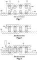
- a first electronic component 10a provided with solder balls 12a on one of its faces 14a is aligned with a second electronic component 10b , also provided with solder balls 12b on one of its faces 14b.
- Pressure is then exerted on the second component according to the illustrated arrows further raising the temperature of the assembly to a temperature greater than or equal to the melting temperature of the constituent metal of the balls 12a, 12b.
- the balls 12a, 12b then solidify with each other by thermocompression to form interconnections 16 ( figure 2 ).
- an electrically insulating liquid resin 18 is deposited using a distributor 20 on the face 14a of the first component 10a.
- the resin 18 migrates by capillarity into the volume 20 between the facing surfaces of the faces 14a, 14b parallel and eventually completely fill the volume 20, thus embedding the electrical interconnects 16 ( figure 4 ).
- the resin 18 is then solidified, usually by applying a heat treatment, or " curing ".
- a last step of connecting the hybridized device with external elements is then implemented ( figure 5 ), for example by connecting connection pads 22, provided for this purpose on the first component 10a, by son 24 (connections called " wire-bonding ").
- the resin is a mixture of a glue as a main component, for example an epoxy glue, and a solvent which makes it possible to adjust the viscosity of the resin and which is evaporated during the heat treatment. of the resin.
- the mixture may also comprise curing agents, especially polymerization agents, for example a catalyst, a photoinitiator or a thermo-initiator, and / or surfactants, for example silane, which increases the adhesion and the wettability of the resin on the surfaces of the components with which it comes into contact, and / or particles to adjust the coefficient of thermal expansion of the resin, usually referred to as " fillers " .
- the first problem posed by the "flip chip coated” technique is that of the presence of a polymer in the filler resin.
- polymers are inherently “non-hermetic", that is to say that they can not constitute in the long term a barrier against moisture.
- their effectiveness against moisture greatly degrades when the device undergoes significant thermal excursions. More particularly, corrosion of the interconnections 16 is observed in the presence of adsorbed moisture.
- the interconnections consist generally of a complex stack of metallic materials (welds, intermetallics, bonding metals, barrier metals to the diffusion of the welds, etc ...), so that these structures have chemical potentials conducive to accelerated corrosion in the presence of moisture.
- the moisture involves the swelling of the coating resins after absorption of moisture, which induces mechanical forces tending to separate the components and leading to the premature rupture of the interconnections 16.
- the only coating material of the state of the art does not allow good resistance to climatic stresses.
- the object of the present invention is to provide increased moisture resistance interconnections connecting two components reported on one another, particularly in the context of a hybridization type "flip-chip".
- the method comprises applying a deposit of atomic thin layers to the device so as to form a layer of mineral material covering at least said interconnection elements, the layer of mineral material having a vapor permeability less than or equal to 10 -3 g / m 2 / day.
- inorganic material is understood to mean inorganic or ceramic materials having ionic bonds and / or covalent bonds, in particular inorganic materials characterized by their mechanical and thermal resistance (eg refractory materials) and their good barrier quality. water vapor.
- mineral materials used as waterproofing electrical interconnections include oxides and / or dielectric nitride, including those of formulas TiO 2 , ZrO 2 , SiO x , SiN x , SiO x N y , ZnSe, ZnO, Sb 2 O 3 , aluminum oxides (eg Al 2 O 3 ), and transparent conductive oxides (or "OTCs", eg indium tin oxide (“ITO”) or zinc oxide doped with aluminum (“AZO”)).
- oxides and / or dielectric nitride including those of formulas TiO 2 , ZrO 2 , SiO x , SiN x , SiO x N y , ZnSe, ZnO, Sb 2 O 3 , aluminum oxides (eg Al 2 O 3 ), and transparent conductive oxides (or "OTCs", eg indium tin oxide (“ITO”) or zinc oxide doped with aluminum (“AZO”)).
- ITO indium t
- the invention consists in waterproofing the interconnections of two components, for example assembled according to a "flip-chip” technique, this waterproofing occurring after the hybridization but before coating with the resin.
- the surface of the interconnections is thus covered with a mineral material, and therefore a material which is both non-corrodible by water and which forms an effective barrier to water.
- the waterproofing material has a form of adhesion with metals.
- interconnections that are located in a volume having a very large aspect ratio.
- the interconnections have such a high surface density that there is no "direct" path from the edge of the hybrid device, ie the point of entry of the vapor into the volume between the two components, and the interconnections housed in the heart of the device.
- the coating is always made in the liquid phase, using the capillarity for its progression between the two components.
- the inventors have succeeded in depositing a layer of mineral material on interconnections housed in a volume of aspect ratio greater than or equal to 10 3 (this value corresponding, for example, to facing surfaces which are square with one side of 10 millimeters and spaced 10 microns apart) with surface densities of interconnections greater than 10 10 / m 2 .
- the layer of mineral material material has a thickness of between 10 nanometers and 100 nanometers, in particular for a mineral material consisting of alumina (Al 2 O 3 ).
- a thickness of 10 nanometers allows a good waterproofing of the interconnections. It is further noted that beyond 100 nm no significant gain in terms of impermeability is obtained.
- the enclosure is not traversed by a continuous flow of the precursors used by the ALD deposit, as is conventionally the case of an ALD deposit.
- the species may not have time to diffuse everywhere in the asperities that represent the inter-component volume and interconnections.
- there may also exist gas flows disturbed by these asperities vortex generation for example), giving rise to a non-homogeneous deposited layer, or even to uncovered portions.
- the species By stopping the pumping, the species have time to diffuse without producing gas disturbance.
- the method comprises the deposition of a filling material completely filling the empty space of material separating the facing surfaces of the two components, the deposition of the filling material being carried out after the deposition of the coating layer. mineral material on the interconnecting elements.
- this device comprises a layer of mineral material covering at least said interconnection elements, the layer of mineral material having a permeability to water vapor less than or equal to 10 -3 g / m 2 / day.
- Such a device is much more reliable against corrosion of these interconnections and thus has a longer life.
- the inorganic material is chosen from the group consisting of compounds of formula SiO x , SiN x , SiO x N y , ZnSe, ZnO, Sb 2 O 3 , aluminum oxides and transparent conductive oxides ( OTC).
- the layer of mineral material has a thickness of between 10 nanometers and 100 nanometers.
- the device comprises a filling material completely filling the space separating the facing surfaces of the two components.
- a method of manufacturing a device 30 comprising two electronic components 10a, 10b , hybridized and having electrical interconnections 16, starts in a manner similar to the state of the art, such as for example described in connection with the Figures 1 and 2 .
- This device comprises two electronic components, for example separated by a distance of between 1 micrometer and 10 micrometers, whose facing area is greater than 100 mm 2 (for example two square surfaces of 10 mm side opposite one on the other), and whose surface density of interconnections is between 10 10 / m 2 and 10 12 / m 2 .
- the device 30 is placed in the chamber, in particular on a support 32, and the injection of the precursors is carried out without pumping, so that the precursors bathe the device 30 and diffuse integrally in the volume 20 between the components 10a, 10b without causing gas disturbance.
- the layer of mineral material deposited by ALD is advantageously an electrically insulating layer, in particular a layer of material of formula TiO 2 , ZrO 2 , SiO x , SiN x , SiO x N y , ZnSe, ZnO, Sb 2 O 3 , the oxides of aluminum (eg Al 2 O 3 ) and transparent conductive oxides (or "OTC", eg indium tin oxide (“ITO”) or zinc oxide doped with aluminum (“AZO" )), especially with a thickness of between 10 nanometers and 100 nanometers. It is thus obtained a layer whose permeability to water vapor is less than or equal to 10 -3 g / m 2 / day.
- a layer of Al 2 O 3 , TiO 2 or ZrO 2 is deposited.
- These materials in addition to their waterproofing property, have good wettability with the resins usually used for filling, and thus help the progression by capillarity of the resin.
- the layer 34 consists of a single material.
- the layer 34 is a multilayer of different mineral materials, called nano-laminates, which makes it possible to combine different properties of permeability, or to block paths of diffusion of the gases in a layer by the deposition of a layer of different material.
- the layer 34 is an Al 2 O 3 / TiO 2 bilayer or an Al 2 O 3 / ZrO 2 bilayer.
- a bilayer makes it possible to passivate the layer in contact with the interconnections (eg Al 2 O 3 ) with a material that is stable to humidity.
- connection pads 22 of the device are not accessible to an electrical connection, in particular by wire-bonding.
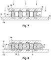
- the method is therefore continued by the release of at least one of these connection pads 22, advantageously by the implementation of an isotropic attack, of normal direction to the main plane of the device, as illustrated by the arrows of the figure 7 .
- This isotropic etching has the effect of removing the portions of impermeable layers on the upper face of the second component 10b and the impervious layer portions 34 of the first component 10a which are not facing the second component 10b , and consequently the portions of layer 34 covering the connection pads 22.
- the isotropic etching is for example an ionic machining (unidirectional ion bombardment), an isotropic plasma etching, etc. If necessary, the lateral edges 36 of the device are also released, for example by tilting the device 30 during the isotropic attack, while preventing the attack from reaching the interconnections 16.
- the manufacturing process continues in the conventional manner by filling the inter-component volume 20 by resin 18 and connecting pads 22, for example as described in relation to Figures 3 to 5 .
- the interconnections of which are encapsulated by an impermeable layer 34 and whose volume 20 between the electronic components 10a and 10b is filled with resin 18 ( figure 8 ).
- the waterproofing process was tested on the display of a projector comprising a matrix of 1746 ⁇ 1000 pixels (and therefore as many interconnections) at a pitch of 10 micrometers, hybridized on a matrix of CMOS control provided with micro-tubes coated with a gold layer and respectively inserted into the indium balls of the matrix of pixels, the interconnections thus being constituted by micro-tubes inserted into balls.
- the size of the active matrix is thus 17.46 mm by 10 mm and the matrix of pixels is spaced from the control matrix by a distance of 5 micrometers.
- Such hybridization is described for example in the documents WO 2009/115686 and US 2011/0094789 .
- a layer of 25 nanometers of Al 2 O 3 was deposited by ALD on each of the interconnections, the process ending in the coating by capillarity using a resin for example of the "Epotek 353ND” ⁇ from Epoxy Technology Inc., USA.
- the invention applies to any type of hybridization "flip-chip” (thermocompression of balls, insertion of male elements in female elements, insertion of solid or hollow elements in balls of lower ductility, insertion at ambient temperature or not, etc ).
- the invention applies to any device having two components facing each other and connected by interconnections, electrical or otherwise, the device was obtained by hybridization "flip-chip" or not.
- the invention also covers devices which do not have such a coating.
Abstract
Ce procédé concerne la protection contre l'humidité d'un dispositif comportant un premier et un second composants électroniques (10a, 10b) présentant respectivement deux surfaces en regard, lesdites surfaces :
- étant séparées par une distance non nulle et inférieure à 10 micromètres ;
- ayant une aire supérieure à 100 mm2 ;
- étant connectées par un ensemble d'éléments d'interconnexion électriques (16) espacés les uns des autres par un espace vide de matière,This method relates to the protection against moisture of a device comprising a first and a second electronic component (10a, 10b) respectively having two facing surfaces, said surfaces:
- being separated by a non-zero distance and less than 10 micrometers;
- having an area greater than 100 mm 2 ;
- being connected by a set of electrical interconnection elements (16) spaced apart from one another by an empty space of material,
Ce procédé comporte l'application d'un dépôt de couches minces atomiques au dispositif de manière à former une couche (34) de matériau minéral recouvrant au moins lesdits éléments d'interconnexion, la couche de matériau minéral ayant une perméabilité à la vapeur d'eau inférieure ou égale à 10-3 g/m2/jour.

Description
La présente invention a trait à la fiabilisation de connexions entre deux composants assemblés.The present invention relates to the reliability of connections between two assembled components.
L'invention trouve plus particulièrement application dans l'assemblage de deux composants électroniques selon la technique dite « face contre face », mieux connue sous l'expression anglo-saxonne « flip chip », qui réalise des interconnexions verticales entre les deux composants. L'invention trouve ainsi particulièrement application dans les assemblages dits « puce sur puce », « puce sur wafer » et « wafer sur wafer ».The invention is more particularly applicable in the assembly of two electronic components according to the so-called "face-to-face" technique, better known by the Anglo-Saxon " flip chip ", which provides vertical interconnections between the two components. The invention thus finds particular application in assemblies known as "chip on chip", "chip on wafer" and "wafer on wafer".
L'invention s'applique avantageusement aux dispositifs requérant des interconnexions de motifs métalliques à très petits pas, notamment pour la fabrication d'imageurs de très grandes dimensions et à très petits pas, comme par exemple les matrices de détection hétérogènes de grande taille comprenant un grand nombre de connexions, des matrices de détection sensibles à la température et hybridées à froid, ou encore des matrices de détection sensibles aux contraintes mécaniques. L'invention s'applique également avantageusement aux structures dites « 3D », qui comprennent un empilement de circuits constitués de matériaux différents et par conséquent sensibles aux contraintes thermiques. L'invention s'applique également particulièrement aux détecteurs à forte sensibilité, capables de détecter un nombre restreint de photons, notamment un photon unique.The invention is advantageously applicable to devices requiring interconnections of metal units with very small steps, in particular for the production of imagers of very large dimensions and with very small steps, such as, for example, large heterogeneous detection matrices comprising a a large number of connections, temperature-sensitive and cold-hybridized detection matrices, or detection matrices sensitive to mechanical stresses. The invention also advantageously applies to so-called "3D" structures, which comprise a stack of circuits made of different materials and therefore sensitive to thermal stresses. The invention is also particularly applicable to high sensitivity detectors capable of detecting a limited number of photons, in particular a single photon.
L'invention s'applique également à l'hybridation à froid de composants.The invention is also applicable to the cold hybridization of components.
L'assemblage de deux composants électroniques par la technique dite « flip chip », par exemple par thermocompression, consiste usuellement à former des billes de soudure électriquement conductrices sur une face d'un premier composant électronique et sur une face d'un second composant selon un motif de connexion prédéterminé. Le premier composant est alors reporté sur le second composant de manière à mettre en correspondance les billes respectives de soudure de ceux-ci, puis l'ensemble est pressé et chauffé. Les billes mises en contact se déforment et fondent pour former des interconnexions électriques perpendiculaires au plan principal des composants électroniques, généralement sous la forme d'une tranche.The assembly of two electronic components by the so-called " flip chip " technique, for example by thermocompression, usually consists of forming electrically conductive solder balls on one face of a first electronic component and on one side of a second component according to a predetermined connection pattern. The first component is then transferred to the second component so as to match the respective solder balls thereof, then the assembly is pressed and heated. The contacted beads deform and melt to form electrical interconnections perpendicular to the main plane of the electronic components, usually in the form of a wafer.
Il est ainsi généralement obtenu un dispositif comportant deux composants électroniques séparés d'une distance comprise entre 1 micromètre et 10 micromètres, dont l'aire en regard est supérieure à 100 mm2 (par exemple deux surfaces carrées de 10 millimètres de coté en regard l'une de l'autre). Usuellement, la densité surfacique d'interconnexions est comprise entre 1010/m2 et 1012/m2.It is thus generally obtained a device comprising two electronic components separated by a distance of between 1 micrometer and 10 micrometers, the facing area of which is greater than 100 mm 2 (for example two square surfaces of 10 millimeters on the side opposite the one of the other). Usually, the surface density of interconnections is between 10 10 / m 2 and 10 12 / m 2 .
Un problème avec ce type d'assemblage est que les interconnexions verticales obtenues par l'hybridation sont sensibles aux contraintes thermiques, et ce d'autant plus que les premier et second composants sont constitués de matériaux différents. En effet, les composants présentent le plus souvent des coefficients d'expansion thermique différents, de sorte que sous l'effet d'une variation de température, les interconnexions sont soumises à un cisaillement qui les fragilise et les casse.A problem with this type of assembly is that the vertical interconnections obtained by the hybridization are sensitive to thermal stresses, especially since the first and second components consist of different materials. Indeed, the components most often have different coefficients of thermal expansion, so that under the effect of a temperature variation, the interconnections are subjected to a shear which weakens them and breaks them.
Afin d'accroître la fiabilité thermo-mécanique d'un ensemble hybridé et de fournir une protection des interconnexions contre l'environnement, il est généralement prévu de remplir l'espace séparant les deux composants par une couche de résine, connue sous le nom de résine « d'enrobage » ou d'« underfill », l'action de remplir cet espace étant connue sous le nom d « underfilling ». Les forces de cisaillement sont ainsi réparties sur l'ensemble de la couche séparant les deux composants hybridés, et non plus uniquement sur les interconnexions, ces dernières étant donc protégées de manière efficace. On parle alors de « flip-chip enrobé ». On pourra par exemple se référer au document
On connait deux techniques de remplissage du volume séparant les deux composants hybridés par des billes de soudure : la première est connue sous l'expression de « fast flow », et la seconde est connue sous l'expression de « no-flow ». Ces techniques sont par exemple décrites dans le document
Un assemblage « flip-chip » suivi d'un enrobage selon la technique « fast flow » est à présent décrit en relation avec les
Dans une première étape (
Comme cela est connu en soi, la résine est un mélange d'une colle en tant que composant principal, par exemple une colle époxy, et d'un solvant qui permet de régler la viscosité de la résine et qui est évaporé lors du traitement thermique de la résine. Le mélange peut également comporter des agents durcisseur, notamment de polymérisation, par exemple un catalyseur, un photo-initiateur ou un thermo-initiateur, et/ou des agents de surface, par exemple du silane, qui augmente l'adhésion et la mouillabilité de la résine sur les surfaces des composants avec lesquelles elle rentre en contact, et/ou des particules pour régler le coefficient d'expansion thermique de la résine, usuellement désignées sous le terme de « fillers ». As is known per se, the resin is a mixture of a glue as a main component, for example an epoxy glue, and a solvent which makes it possible to adjust the viscosity of the resin and which is evaporated during the heat treatment. of the resin. The mixture may also comprise curing agents, especially polymerization agents, for example a catalyst, a photoinitiator or a thermo-initiator, and / or surfactants, for example silane, which increases the adhesion and the wettability of the resin on the surfaces of the components with which it comes into contact, and / or particles to adjust the coefficient of thermal expansion of the resin, usually referred to as " fillers " .
Le premier problème posé par la technique « flip chip enrobée » est celui de la présence d'un polymère dans la résine de remplissage. Or, les polymères sont par nature « non hermétiques », c'est-à-dire qu'ils ne peuvent pas constituer sur le long terme une barrière contre l'humidité. En outre, leur efficacité contre l'humidité se dégrade fortement lorsque le dispositif subit des excursions thermiques importantes. Plus particulièrement, on observe une corrosion des interconnexions 16 en présence de l'humidité adsorbée. En effet, les interconnexions sont constituées en général d'un empilement complexe de matériaux métalliques (soudures, intermétalliques, métaux d'accroche, métaux barrière à la diffusion des soudures, etc...), de sorte que ces structures présentent des potentiels chimiques propices à une corrosion accélérée en présence d'humidité.The first problem posed by the "flip chip coated" technique is that of the presence of a polymer in the filler resin. However, polymers are inherently "non-hermetic", that is to say that they can not constitute in the long term a barrier against moisture. In addition, their effectiveness against moisture greatly degrades when the device undergoes significant thermal excursions. More particularly, corrosion of the
Par ailleurs, l'humidité implique le gonflement des résines d'enrobage après absorption d'humidité, ce qui induit des efforts mécaniques tendant à séparer les composants et conduisant à la rupture prématurée des interconnexions 16. Furthermore, the moisture involves the swelling of the coating resins after absorption of moisture, which induces mechanical forces tending to separate the components and leading to the premature rupture of the
Ainsi, le seul matériau d'enrobage de l'état de la technique ne permet pas une bonne résistance à des stress climatiques.Thus, the only coating material of the state of the art does not allow good resistance to climatic stresses.
Le but de la présente invention est de proposer une résistance à l'humidité accrue des interconnexions reliant deux composants reportés l'un sur l'autre, notamment dans le cadre d'une hybridation de type « flip-chip ».The object of the present invention is to provide increased moisture resistance interconnections connecting two components reported on one another, particularly in the context of a hybridization type "flip-chip".
A cet effet, l'invention a pour objet un procédé de protection contre l'humidité d'un dispositif comportant un premier et un second composants électroniques présentant respectivement deux surfaces en regard, lesdites surfaces :
- étant séparées par une distance non nulle et inférieure à 10 micromètres ;
- ayant une aire supérieure à 100 mm2; et
- étant connectées par un ensemble d'éléments d'interconnexion électriques espacés les uns des autres par un espace vide de matière.
- being separated by a non-zero distance and less than 10 micrometers;
- having an area greater than 100 mm 2 ; and
- being connected by a set of electrical interconnection elements spaced from each other by an empty space of material.
Selon l'invention, le procédé comporte l'application d'un dépôt de couches minces atomiques au dispositif de manière à former une couche de matériau minéral recouvrant au moins lesdits éléments d'interconnexion, la couche de matériau minéral ayant une perméabilité à la vapeur d'eau inférieure ou égale à 10-3 g/m2/jour.According to the invention, the method comprises applying a deposit of atomic thin layers to the device so as to form a layer of mineral material covering at least said interconnection elements, the layer of mineral material having a vapor permeability less than or equal to 10 -3 g / m 2 / day.
Par matériau minéral, on entend au sens de l'invention les matériaux minéraux ou céramiques présentant des liaisons ioniques et ou des liaisons covalentes, notamment des matériaux inorganiques caractérisés par leur résistance mécanique et thermique (e.g. matériaux réfractaires) et leur bonne qualité de barrière à la vapeur d'eau. Parmi les matériaux minéraux utilisés comme imperméabilisant des interconnexions électriques, on peut citer les oxydes et/ou nitrure diélectrique, notamment ceux de formules TiO2, ZrO2, SiOx, SiNx, SiOxNy, ZnSe, ZnO, Sb2O3, les oxydes d'aluminium (e.g. Al2O3), et les oxydes transparents conducteurs (ou « OTC », e.g. l'oxyde d'indium-étain (« ITO ») ou l'oxyde de zinc dopés à l'aluminium (« AZO »)).For the purposes of the invention, inorganic material is understood to mean inorganic or ceramic materials having ionic bonds and / or covalent bonds, in particular inorganic materials characterized by their mechanical and thermal resistance (eg refractory materials) and their good barrier quality. water vapor. Among the mineral materials used as waterproofing electrical interconnections include oxides and / or dielectric nitride, including those of formulas TiO 2 , ZrO 2 , SiO x , SiN x , SiO x N y , ZnSe, ZnO, Sb 2 O 3 , aluminum oxides (eg Al 2 O 3 ), and transparent conductive oxides (or "OTCs", eg indium tin oxide ("ITO") or zinc oxide doped with aluminum ("AZO")).
En d'autres termes, l'invention consiste à imperméabiliser les interconnexions de deux composants, par exemple assemblés selon une technique « flip-chip », cette imperméabilisation intervenant après l'hybridation mais avant l'enrobage par la résine. La surface des interconnexions est ainsi recouverte d'un matériau minéral, et par conséquent un matériau qui est à la fois non corrodable par l'eau et qui forme une barrière efficace à l'eau. En outre, le matériau imperméabilisant présente une formte adhérence avec les métaux. Enfin, les interconnexions n'étant pas corrodées, elles résistent donc mieux au gonflement résine induite par l'humidité.In other words, the invention consists in waterproofing the interconnections of two components, for example assembled according to a "flip-chip" technique, this waterproofing occurring after the hybridization but before coating with the resin. The surface of the interconnections is thus covered with a mineral material, and therefore a material which is both non-corrodible by water and which forms an effective barrier to water. In addition, the waterproofing material has a form of adhesion with metals. Finally, since the interconnections are not corroded, they are therefore more resistant to humidity-induced resin swelling.
En outre, il est considéré que les techniques classiques de dépôt en phase vapeur (e.g. PVD, CVD, mais également ALD) ne sont pas adaptées pour revêtir les interconnexions qui sont localisées dans un volume présentant un très grand rapport d'aspect. En effet, les interconnexions ont une densité surfacique si élevée qu'il n'existe pas de chemin « direct » depuis le bord du dispositif hybridé, i.e. le point d'entrée de la vapeur dans le volume entre les deux composants, et les interconnexions logées au coeur du dispositif. Notamment, pour chacune de ces interconnexions, il existe une multitude d'interconnexions qui la masquent de la phase vapeur. On note d'ailleurs que l'enrobage est toujours réalisé en phase liquide, utilisant la capillarité pour sa progression entre les deux composants. Notamment, il n'a pas été proposé dans l'état de la technique d'utiliser des techniques de dépôt en phase vapeur pour l'enrobage, alors même que ces techniques sont capables de déposer des épaisseurs de matériau de plusieurs dizaines de micromètres, et donc des épaisseurs bien supérieure à la distance usuelle entre les deux composants hybridés (de 1µm à 10 µm). Ceci signifie notamment qu'il est considéré que le volume entre les deux composants entrecoupés d'une multitudes d'interconnexions n'est accessible que par capillarité, les dépôts en phase vapeur étant au contraire utilisés pour déposer ou remplir des cavités vides de toute matière qui offrent des chemins directs à leurs parois pour la phase vapeur.In addition, it is considered that conventional vapor deposition techniques (e.g. PVD, CVD, but also ALD) are not suitable for coating interconnections that are located in a volume having a very large aspect ratio. In fact, the interconnections have such a high surface density that there is no "direct" path from the edge of the hybrid device, ie the point of entry of the vapor into the volume between the two components, and the interconnections housed in the heart of the device. In particular, for each of these interconnections, there is a multitude of interconnections that mask the vapor phase. It should also be noted that the coating is always made in the liquid phase, using the capillarity for its progression between the two components. In particular, it has not been proposed in the state of the art to use vapor deposition techniques for coating, even though these techniques are capable of depositing material thicknesses of several tens of micrometers, and therefore much greater thicknesses than the usual distance between the two hybridized components (from 1 .mu.m to 10 .mu.m). This means that it is considered that the volume between the two components interspersed with a multitude of interconnections is accessible only by capillarity, the vapor phase deposits being instead used to deposit or fill empty cavities of any material which offer direct paths to their walls for the vapor phase.
Or, les inventeurs sont parvenus à déposer une couche de matériau minéral sur des interconnexions logées dans un volume de rapport d'aspect supérieur ou égal à 103 (cette valeur correspondant par exemple à des surfaces en regard qui sont carrées avec un côté de 10 millimètres et qui sont espacées de 10 micromètres) avec des densités surfaciques d'interconnexions supérieures à 1010/m2.However, the inventors have succeeded in depositing a layer of mineral material on interconnections housed in a volume of aspect ratio greater than or equal to 10 3 (this value corresponding, for example, to facing surfaces which are square with one side of 10 millimeters and spaced 10 microns apart) with surface densities of interconnections greater than 10 10 / m 2 .
Selon un mode de réalisation particulier, la couche de matériau de matériau minéral a une épaisseur comprise entre 10 nanomètres et 100 nanomètres, en particulier pour un matériau minéral constitué d'alumine (Al2O3). Une épaisseur de 10 nanomètre permet une bonne imperméabilisation des interconnexions. On constate en outre qu'au-delà de 100 nanomètre aucun gain notable en termes d'imperméabilité n'est obtenu.According to a particular embodiment, the layer of mineral material material has a thickness of between 10 nanometers and 100 nanometers, in particular for a mineral material consisting of alumina (Al 2 O 3 ). A thickness of 10 nanometers allows a good waterproofing of the interconnections. It is further noted that beyond 100 nm no significant gain in terms of impermeability is obtained.
Selon un mode de réalisation :
- l'application du dépôt de couches minces atomiques comprend le placement de la structure dans une enceinte et l'injection dans ladite enceinte de gaz réactifs pour la formation de la couche de matériau minéral ;
- et l'injection des gaz réactifs est réalisée sans pompage de l'enceinte.
- the application of the atomic thin film deposition comprises the placement of the structure in a chamber and the injection into said chamber of reactive gases for the formation of the layer of mineral material;
- and the injection of the reactive gases is carried out without pumping the enclosure.
En d'autres termes, lors du dépôt, l'enceinte n'est pas parcourue par un écoulement continu des précurseurs utilisés par le dépôt ALD, comme cela est classiquement le cas d'un dépôt ALD. En effet, dans ce mode de fonctionnement classique avec pompage, les espèces peuvent ne pas avoir le temps de diffuser partout dans les aspérités que représentent le volume inter-composants et les interconnexions. En outre, il peut également exister des écoulements de gaz perturbés par ces aspérités (génération de vortex par exemple), donnant naissance à une couche déposée non homogène, voire même à des portions non recouvertes. En stoppant le pompage, les espèces ont donc le temps de diffuser sans produire de perturbation gazeuse.In other words, during the deposition, the enclosure is not traversed by a continuous flow of the precursors used by the ALD deposit, as is conventionally the case of an ALD deposit. Indeed, in this conventional mode of operation with pumping, the species may not have time to diffuse everywhere in the asperities that represent the inter-component volume and interconnections. In addition, there may also exist gas flows disturbed by these asperities (vortex generation for example), giving rise to a non-homogeneous deposited layer, or even to uncovered portions. By stopping the pumping, the species have time to diffuse without producing gas disturbance.
Selon un mode de réalisation optionnel, le procédé comprend le dépôt d'un matériau de remplissage remplissant complètement l'espace vide de matière séparant les surfaces en regard des deux composants, le dépôt du matériau de remplissage étant réalisé après le dépôt de la couche de matériau minéral sur les éléments d'interconnexion.According to an optional embodiment, the method comprises the deposition of a filling material completely filling the empty space of material separating the facing surfaces of the two components, the deposition of the filling material being carried out after the deposition of the coating layer. mineral material on the interconnecting elements.
L'invention a également pour objet un dispositif comportant un premier et un second composants électroniques présentant respectivement deux surfaces en regard, lesdites surfaces :
- étant séparées par une distance non nulle et inférieure à 10 micromètres ;
- ayant une aire supérieure à 100 mm2;
- étant connectées par un ensemble d'éléments d'interconnexion électriques distincts.
- being separated by a non-zero distance and less than 10 micrometers;
- having an area greater than 100 mm 2 ;
- being connected by a set of separate electrical interconnection elements.
Selon l'invention, ce dispositif comporte une couche de matériau minéral recouvrant au moins lesdits éléments d'interconnexion, la couche de matériau minéral ayant une perméabilité à la vapeur d'eau inférieure ou égale à 10-3 g/m2/jour.According to the invention, this device comprises a layer of mineral material covering at least said interconnection elements, the layer of mineral material having a permeability to water vapor less than or equal to 10 -3 g / m 2 / day.
Un tel dispositif est beaucoup plus fiable contre la corrosion de ces interconnexions et présente ainsi une durée de vie accrue.Such a device is much more reliable against corrosion of these interconnections and thus has a longer life.
Selon un mode de réalisation, le matériau minéral est choisi dans le groupe constitué par les composés de formule SiOx, SiNx, SiOxNy, ZnSe, ZnO, Sb2O3, les oxydes d'aluminium et les oxydes transparents conducteurs (OTC).According to one embodiment, the inorganic material is chosen from the group consisting of compounds of formula SiO x , SiN x , SiO x N y , ZnSe, ZnO, Sb 2 O 3 , aluminum oxides and transparent conductive oxides ( OTC).
Selon un mode de réalisation, la couche de matériau minéral a une épaisseur comprise entre 10 nanomètres et 100 nanomètres.According to one embodiment, the layer of mineral material has a thickness of between 10 nanometers and 100 nanometers.
Selon un mode de réalisation, le dispositif comprend un matériau de remplissage remplissant complètement l'espace séparant les surfaces en regard des deux composants.According to one embodiment, the device comprises a filling material completely filling the space separating the facing surfaces of the two components.
La présente invention sera mieux comprise à la lecture de la description qui va suivre, donnée uniquement à titre d'exemple, et réalisée en relation avec les dessins annexés, dans lesquels des références identiques désignent des éléments identiques, et dans lesquels :
- les
figures 1 à 5 sont des vues schématiques en coupe illustrant un procédé de fabrication d'un dispositif hybridé par une technique « flip-chip » selon l'état de la technique, tel que discuté ci-avant ; et - les
figures 6 à 8 sont des vues schématiques en coupe illustrant un procédé de fabrication d'un dispositif hybridé par une technique « flip-chip » selon l'invention, comprenant une étape d'imperméabilisation des interconnexions électriques.
- the
Figures 1 to 5 are diagrammatic sectional views illustrating a method of manufacturing a hybridized device by a "flip-chip" technique according to the state of the art, as discussed above; and - the
Figures 6 to 8 are schematic sectional views illustrating a method of manufacturing a hybridized device by a "flip-chip" technique according to the invention, comprising a step of waterproofing the electrical interconnections.
En se référant aux
Une fois l'hybridation terminée, et avant l'application d'un matériau d'enrobage 18, une étape d'imperméabilisation des interconnexions électriques 16 par une couche minérale est mise en oeuvre au moyen d'un dépôt « ALD ».Once the hybridization is complete, and before the application of a
Comme cela est connu en soi, l'ALD est une technique de dépôt de couches atomiques qui consiste à exposer successivement une surface placée dans une enceinte, ou « chambre à réaction », à différents précurseurs chimiques, afin d'obtenir des couches ultra minces. Le dépôt d'une couche atomique se déroule usuellement en 4 étapes :
- a) injection dans la chambre d'un premier précurseur gazeux entrainant la formation sur la surface d'une monocouche constituée d'espèces chimisorbées et d'autres physisorbées ;
- b) purge de la chambre de réaction, par exemple au moyen d'un balayage par de l'azote ultra pur pour éliminer toutes espèces n'ayant pas réagi ainsi que d'éventuels sous-produits de réaction ;
- c) injection dans la chambre d'un second précurseur gazeux entrainant la formation de la couche de matériau souhaité sur la surface ;
- d) purge de la chambre pour éliminer les espèces n'ayant pas réagi et les éventuels sous-produits de réaction. Classiquement, un pompage de l'enceinte est mis en oeuvre pendant l'injection des précurseurs afin de produire un écoulement de ces derniers dans l'enceinte.
- a) injection into the chamber of a first gaseous precursor resulting in the formation on the surface of a monolayer consisting of chemisorbed species and other physisorbed species;
- b) purge the reaction chamber, for example by means of a purge with ultra pure nitrogen to remove all unreacted species and any reaction by-products;
- c) injecting into the chamber a second gaseous precursor causing the formation of the desired layer of material on the surface;
- d) purging the chamber to remove unreacted species and any reaction by-products. Conventionally, a pumping of the chamber is implemented during the injection of the precursors to produce a flow of the latter in the enclosure.
De manière avantageuse, le dispositif 30 est placé dans l'enceinte, notamment sur un support 32, et l'injection des précurseurs est réalisée sans pompage, de sorte que les précurseurs baignent le dispositif 30 et diffusent intégralement dans le volume 20 entre les composants 10a, 10b sans provoquer de perturbation gazeuse. Il est ainsi obtenu une couche 34 déposée sur l'intégralité de la surface exposée du dispositif 30, et donc sur les interconnexions 16 (
La couche de matériau minéral déposée par ALD est avantageusement une couche électriquement isolante, notamment une couche de matériau de formule TiO2, ZrO2, SiOx, SiNx, SiOxNy, ZnSe, ZnO, Sb2O3, les oxydes d'aluminium (e.g. Al2O3) et les oxydes transparents conducteurs (ou « OTC », e.g. l'oxyde d'indium-étain (« ITO ») ou l'oxyde de zinc dopés à l'aluminium (« AZO »)), notamment d'une épaisseur comprise entre 10 nanomètres et 100 nanomètres. Il est ainsi obtenu une couche dont la perméabilité à la vapeur d'eau inférieure ou égale à 10-3 g/m2/jour.The layer of mineral material deposited by ALD is advantageously an electrically insulating layer, in particular a layer of material of formula TiO 2 , ZrO 2 , SiO x , SiN x , SiO x N y , ZnSe, ZnO, Sb 2 O 3 , the oxides of aluminum (eg Al 2 O 3 ) and transparent conductive oxides (or "OTC", eg indium tin oxide ("ITO") or zinc oxide doped with aluminum ("AZO" )), especially with a thickness of between 10 nanometers and 100 nanometers. It is thus obtained a layer whose permeability to water vapor is less than or equal to 10 -3 g / m 2 / day.
De manière avantageuse, une couche d'Al2O3, de TiO2 ou de ZrO2 est déposée. Ces matériaux, outre leur propriété imperméabilisante, présente une bonne mouillabilité avec les résines usuellement utilisées pour le remplissage, et aide donc à la progression par capillarité de la résine..Advantageously, a layer of Al 2 O 3 , TiO 2 or ZrO 2 is deposited. These materials, in addition to their waterproofing property, have good wettability with the resins usually used for filling, and thus help the progression by capillarity of the resin.
Dans une première variante, la couche 34 est constituée d'un unique matériau.In a first variant, the
Dans une seconde variante, la couche 34 est un multicouches de matériaux minéraux différents, appelés nano laminés, ce qui permet de combiner différentes propriétés de perméabilité, ou de boucher des chemins de diffusion des gaz dans une couche par le dépôt d'une couche de matériau différent. Avantageusement, la couche 34 est un bicouche Al2O3/TiO2 ou un bicouche Al2O3/ZrO2. Une bicouche permet notamment de passiver la couche au contact des interconnexions (e.g. Al2O3) par un matériau stable à l'humidité.In a second variant, the
En raison du caractère isolant de la couche imperméable 34, les plages de connexion 22 du dispositif ne sont pas accessibles à une connexion électrique, notamment par wire-bonding. Le procédé se poursuit donc par la libération d'au moins l'une de ces plages de connexion 22, avantageusement par la mise en oeuvre d'une attaque isotrope, de direction normale au plan principal du dispositif, tel qu'illustré par les flèches de la
Une fois l'imperméabilisation des interconnexions 16 réalisée, le procédé de fabrication se poursuit de manière classique par le remplissage du volume 20 inter-composant par de la résine 18 et la connexion des plages 22, par exemple tel que décrit en relation avec les
A titre d'exemple numérique, le procédé d'imperméabilisation a été testé sur l'afficheur d'un projecteur comportant une matrice de 1746×1000 pixels (et donc autant d'interconnexions) au pas de 10 micromètres, hybridée sur une matrice de commande CMOS munie de micro-tubes enrobés d'une couche d'or et respectivement insérés dans les billes d'indium de la matrice de pixels, les interconnexions étant donc constituées de micro-tubes insérés dans des billes. La taille de la matrice active est ainsi de 17,46 mm par 10 mm et la matrice de pixels est espacée de la matrice de commande par une distance de 5 micromètres. Une telle hybridation est décrite par exemple dans les documents
A la vue de ce qui précède, on comprend que l'invention s'applique à tout type d'hybridation « flip-chip » (thermocompression de billes, insertion d'éléments mâles dans des éléments femelles, insertion d'éléments pleins ou creux dans des billes de plus faible ductilité, insertion à température ambiante ou non, etc...).In view of the foregoing, it is understood that the invention applies to any type of hybridization "flip-chip" (thermocompression of balls, insertion of male elements in female elements, insertion of solid or hollow elements in balls of lower ductility, insertion at ambient temperature or not, etc ...).
De même, l'invention s'applique à tout dispositif comportant deux composants en regard et reliés par des interconnexions, électriques ou non, que le dispositif ait été obtenu par hybridation « flip-chip » ou non.Similarly, the invention applies to any device having two components facing each other and connected by interconnections, electrical or otherwise, the device was obtained by hybridization "flip-chip" or not.
De même, bien qu'il ait été décrit une étape finale de remplissage (« underfilling »), l'invention couvre également les dispositifs qui ne sont pas pourvus d'un tel enrobage.Likewise, although a final underfilling step has been described, the invention also covers devices which do not have such a coating.
Claims (9)
Applications Claiming Priority (1)
| Application Number | Priority Date | Filing Date | Title |
|---|---|---|---|
| FR1650873A FR3047604B1 (en) | 2016-02-04 | 2016-02-04 | HUMIDITY PROTECTED HYBRID ELECTRONIC DEVICE AND HUMIDITY PROTECTION METHOD OF HYBRID ELECTRONIC DEVICE |
Publications (2)
| Publication Number | Publication Date |
|---|---|
| EP3203511A1 true EP3203511A1 (en) | 2017-08-09 |
| EP3203511B1 EP3203511B1 (en) | 2020-01-29 |
Family
ID=55759811
Family Applications (1)
| Application Number | Title | Priority Date | Filing Date |
|---|---|---|---|
| EP17153660.0A Active EP3203511B1 (en) | 2016-02-04 | 2017-01-30 | Method for protecting a hybrid electronic device against moisture |
Country Status (5)
| Country | Link |
|---|---|
| US (1) | US9793141B2 (en) |
| EP (1) | EP3203511B1 (en) |
| JP (1) | JP7160518B2 (en) |
| KR (1) | KR102608794B1 (en) |
| FR (1) | FR3047604B1 (en) |
Cited By (1)
| Publication number | Priority date | Publication date | Assignee | Title |
|---|---|---|---|---|
| WO2020193903A1 (en) * | 2019-03-25 | 2020-10-01 | Commissariat A L'energie Atomique Et Aux Energies Alternatives | Method of manufacturing a structure |
Families Citing this family (4)
| Publication number | Priority date | Publication date | Assignee | Title |
|---|---|---|---|---|
| US10957672B2 (en) * | 2017-11-13 | 2021-03-23 | Taiwan Semiconductor Manufacturing Company, Ltd. | Package structure and method of manufacturing the same |
| WO2021151684A1 (en) * | 2020-01-28 | 2021-08-05 | Tdk Electronics Ag | Method of manufacturing and passivating a die |
| US20230084360A1 (en) * | 2021-09-10 | 2023-03-16 | Innolux Corporation | Electronic device and manufacturing method thereof |
| EP4213199A1 (en) * | 2022-01-14 | 2023-07-19 | Nexperia B.V. | Chip-scale packaged vertical semiconductor device |
Citations (6)
| Publication number | Priority date | Publication date | Assignee | Title |
|---|---|---|---|---|
| US20050103264A1 (en) * | 2003-11-13 | 2005-05-19 | Frank Jansen | Atomic layer deposition process and apparatus |
| US20090001487A1 (en) * | 2007-06-29 | 2009-01-01 | Fujitsu Limited | Packaged device and method of manufacturing the same |
| US20090065932A1 (en) * | 2007-09-11 | 2009-03-12 | Sandeep Sane | Methods of forming nano-coatings for improved adhesion between first level interconnects and epoxy under-fills in microelectronic packages and structures formed thereby |
| WO2009115686A2 (en) | 2008-02-22 | 2009-09-24 | Commissariat A L'energie Atomique | Connection component with hollow inserts and method for making same |
| EP2476784A1 (en) * | 2011-01-18 | 2012-07-18 | Nederlandse Organisatie voor toegepast -natuurwetenschappelijk onderzoek TNO | Method for manufacturing an electronic device by electrodeposition from an ionic liquid |
| US20160020160A1 (en) * | 2014-07-16 | 2016-01-21 | International Business Machines Corporation | Devices employing semiconductor die having hydrophobic coatings, and related cooling methods |
Family Cites Families (12)
| Publication number | Priority date | Publication date | Assignee | Title |
|---|---|---|---|---|
| US5956605A (en) * | 1996-09-20 | 1999-09-21 | Micron Technology, Inc. | Use of nitrides for flip-chip encapsulation |
| US7164520B2 (en) * | 2004-05-12 | 2007-01-16 | Idc, Llc | Packaging for an interferometric modulator |
| US7972669B2 (en) * | 2005-11-04 | 2011-07-05 | Unitika Ltd. | Biodegradable resin foam sheet, biodegradable resin foam article and biodegradable resin molded container |
| JP4997757B2 (en) * | 2005-12-20 | 2012-08-08 | 富士通株式会社 | Thin film capacitor and method for manufacturing the same, electronic device and circuit board |
| JP2007250572A (en) * | 2006-03-13 | 2007-09-27 | Seiko Epson Corp | Piezoelectric element |
| JP4182996B2 (en) * | 2006-08-10 | 2008-11-19 | ソニー株式会社 | Electronic device and manufacturing method thereof |
| WO2008114413A1 (en) * | 2007-03-20 | 2008-09-25 | Fujitsu Microelectronics Limited | Process for producing semiconductor device |
| JP5239294B2 (en) * | 2007-10-31 | 2013-07-17 | 富士通セミコンダクター株式会社 | Manufacturing method of semiconductor device |
| JP2008113045A (en) * | 2008-02-04 | 2008-05-15 | Texas Instr Japan Ltd | Method for manufacturing semiconductor device |
| JP5210663B2 (en) * | 2008-02-29 | 2013-06-12 | 旭化成株式会社 | Organic EL device |
| JP5250524B2 (en) * | 2009-10-14 | 2013-07-31 | ルネサスエレクトロニクス株式会社 | Semiconductor device and manufacturing method thereof |
| JP5938912B2 (en) * | 2012-01-13 | 2016-06-22 | 日亜化学工業株式会社 | Light emitting device and lighting device |
-
2016
- 2016-02-04 FR FR1650873A patent/FR3047604B1/en not_active Expired - Fee Related
-
2017
- 2017-01-30 JP JP2017013825A patent/JP7160518B2/en active Active
- 2017-01-30 US US15/419,576 patent/US9793141B2/en active Active
- 2017-01-30 EP EP17153660.0A patent/EP3203511B1/en active Active
- 2017-01-31 KR KR1020170013682A patent/KR102608794B1/en active IP Right Grant
Patent Citations (7)
| Publication number | Priority date | Publication date | Assignee | Title |
|---|---|---|---|---|
| US20050103264A1 (en) * | 2003-11-13 | 2005-05-19 | Frank Jansen | Atomic layer deposition process and apparatus |
| US20090001487A1 (en) * | 2007-06-29 | 2009-01-01 | Fujitsu Limited | Packaged device and method of manufacturing the same |
| US20090065932A1 (en) * | 2007-09-11 | 2009-03-12 | Sandeep Sane | Methods of forming nano-coatings for improved adhesion between first level interconnects and epoxy under-fills in microelectronic packages and structures formed thereby |
| WO2009115686A2 (en) | 2008-02-22 | 2009-09-24 | Commissariat A L'energie Atomique | Connection component with hollow inserts and method for making same |
| US20110094789A1 (en) | 2008-02-22 | 2011-04-28 | Commissariat A. L'Energie Atomique et Aux Energies Alternatives | Connection component with hollow inserts and method for making same |
| EP2476784A1 (en) * | 2011-01-18 | 2012-07-18 | Nederlandse Organisatie voor toegepast -natuurwetenschappelijk onderzoek TNO | Method for manufacturing an electronic device by electrodeposition from an ionic liquid |
| US20160020160A1 (en) * | 2014-07-16 | 2016-01-21 | International Business Machines Corporation | Devices employing semiconductor die having hydrophobic coatings, and related cooling methods |
Non-Patent Citations (2)
| Title |
|---|
| C.P. WONG ET AL.: "Characterization of a No-Flow Underfill Encapsulant During the Solder Reflow Process", PROCEEDINGS OF THE ELECTRONIC COMPONENTS AND TECHNOLOY CONFÉRENCE, 1998, pages 1253 - 1259, XP000803705 |
| TONY MAINDRON ET AL: "Investigation of Al2O3 barrier film properties made by atomic layer deposition onto fluorescent tris-(8-hydroxyquinoline) aluminium molecular films", THIN SOLID FILMS, vol. 548, 1 December 2013 (2013-12-01), CH, pages 517 - 525, XP055294322, ISSN: 0040-6090, DOI: 10.1016/j.tsf.2013.08.092 * |
Cited By (2)
| Publication number | Priority date | Publication date | Assignee | Title |
|---|---|---|---|---|
| WO2020193903A1 (en) * | 2019-03-25 | 2020-10-01 | Commissariat A L'energie Atomique Et Aux Energies Alternatives | Method of manufacturing a structure |
| FR3094561A1 (en) * | 2019-03-25 | 2020-10-02 | Commissariat A L'energie Atomique Et Aux Energies Alternatives | Manufacturing process of a structure |
Also Published As
| Publication number | Publication date |
|---|---|
| FR3047604B1 (en) | 2018-02-02 |
| FR3047604A1 (en) | 2017-08-11 |
| JP2017139461A (en) | 2017-08-10 |
| US9793141B2 (en) | 2017-10-17 |
| JP7160518B2 (en) | 2022-10-25 |
| EP3203511B1 (en) | 2020-01-29 |
| US20170229321A1 (en) | 2017-08-10 |
| KR20170093069A (en) | 2017-08-14 |
| KR102608794B1 (en) | 2023-12-01 |
Similar Documents
| Publication | Publication Date | Title |
|---|---|---|
| EP3203511B1 (en) | Method for protecting a hybrid electronic device against moisture | |
| EP0638933B1 (en) | Interconnection process of stacked semi-conductors chips and devices | |
| EP2308797B1 (en) | Structure with a cavity comprising a bonding interface made from a getter material | |
| EP3169625B1 (en) | Method for manufacturing a device comprising a hermetically sealed vacuum housing and getter | |
| EP3613074B1 (en) | Method for joining a microelectronic chip to a wire element | |
| WO1992003902A1 (en) | Method and device for hermetic encapsulation of electronic components | |
| EP3154082B1 (en) | Improved dbc structure provided with a mounting including a phase-change material | |
| EP2829511B1 (en) | Device comprising a fluid channel having at least one micro or nanoelectronic system and method for producing such a device | |
| EP3115129B1 (en) | Assembly comprising an element capable of transmitting heat, highly heat conductive polymer film and electrical insulator, sintered seal and radiator, and method of manufacturing same | |
| FR3007403A1 (en) | METHOD FOR PRODUCING A MECHANICALLY AUTONOMOUS MICROELECTRONIC DEVICE | |
| EP2976784A1 (en) | Flip-chip assembly process comprising pre-coating interconnect elements | |
| EP2171752B1 (en) | Method for coating two elements hybridized by means of a soldering material | |
| FR3055166A1 (en) | INTERCOMPOSING CONNECTION METHOD WITH OPTIMIZED DENSITY | |
| EP2791969B1 (en) | Forming a via electrical connection | |
| EP3165502B1 (en) | Microelectronic device | |
| FR2976719A1 (en) | METHOD FOR PRODUCING A BILAMIC CURVED MICROELECTRONIC COMPONENT, AND MICROELECTRONIC COMPONENT THUS OBTAINED | |
| EP3031775B1 (en) | Method for producing an electrical connection in a blind via | |
| EP3637071A1 (en) | Method for manufacturing an electromagnetic-radiation detection device with improved encapsulation structure | |
| FR3098997A1 (en) | Light emitting device | |
| FR3106695A1 (en) | Process for sealing a microelectronic device | |
| EP4354491A1 (en) | Sip-type electronic device and method for making same | |
| FR2941563A1 (en) | SEALED BARRIER FOR MICROCOMPONENT AND METHOD FOR MANUFACTURING SUCH BARRIER. | |
| FR2848339A1 (en) | Adhesion of two elements comprises nickel-silicon welding at low temperature, for encapsulation of components in integrated circuits and microelectromechanical systems | |
| WO2010037925A2 (en) | Method for encapsulating an organic optoelectronic device |
Legal Events
| Date | Code | Title | Description |
|---|---|---|---|
| PUAI | Public reference made under article 153(3) epc to a published international application that has entered the european phase |
Free format text: ORIGINAL CODE: 0009012 |
|
| STAA | Information on the status of an ep patent application or granted ep patent |
Free format text: STATUS: THE APPLICATION HAS BEEN PUBLISHED |
|
| AK | Designated contracting states |
Kind code of ref document: A1 Designated state(s): AL AT BE BG CH CY CZ DE DK EE ES FI FR GB GR HR HU IE IS IT LI LT LU LV MC MK MT NL NO PL PT RO RS SE SI SK SM TR |
|
| AX | Request for extension of the european patent |
Extension state: BA ME |
|
| STAA | Information on the status of an ep patent application or granted ep patent |
Free format text: STATUS: REQUEST FOR EXAMINATION WAS MADE |
|
| 17P | Request for examination filed |
Effective date: 20171222 |
|
| RBV | Designated contracting states (corrected) |
Designated state(s): AL AT BE BG CH CY CZ DE DK EE ES FI FR GB GR HR HU IE IS IT LI LT LU LV MC MK MT NL NO PL PT RO RS SE SI SK SM TR |
|
| STAA | Information on the status of an ep patent application or granted ep patent |
Free format text: STATUS: EXAMINATION IS IN PROGRESS |
|
| 17Q | First examination report despatched |
Effective date: 20190603 |
|
| GRAP | Despatch of communication of intention to grant a patent |
Free format text: ORIGINAL CODE: EPIDOSNIGR1 |
|
| STAA | Information on the status of an ep patent application or granted ep patent |
Free format text: STATUS: GRANT OF PATENT IS INTENDED |
|
| RIC1 | Information provided on ipc code assigned before grant |
Ipc: H01L 23/31 20060101ALI20190919BHEP Ipc: H01L 23/29 20060101AFI20190919BHEP Ipc: H01L 25/065 20060101ALN20190919BHEP Ipc: H01L 25/00 20060101ALI20190919BHEP |
|
| INTG | Intention to grant announced |
Effective date: 20191004 |
|
| GRAS | Grant fee paid |
Free format text: ORIGINAL CODE: EPIDOSNIGR3 |
|
| GRAA | (expected) grant |
Free format text: ORIGINAL CODE: 0009210 |
|
| STAA | Information on the status of an ep patent application or granted ep patent |
Free format text: STATUS: THE PATENT HAS BEEN GRANTED |
|
| AK | Designated contracting states |
Kind code of ref document: B1 Designated state(s): AL AT BE BG CH CY CZ DE DK EE ES FI FR GB GR HR HU IE IS IT LI LT LU LV MC MK MT NL NO PL PT RO RS SE SI SK SM TR |
|
| REG | Reference to a national code |
Ref country code: GB Ref legal event code: FG4D Free format text: NOT ENGLISH |
|
| REG | Reference to a national code |
Ref country code: CH Ref legal event code: EP |
|
| REG | Reference to a national code |
Ref country code: AT Ref legal event code: REF Ref document number: 1229047 Country of ref document: AT Kind code of ref document: T Effective date: 20200215 |
|
| REG | Reference to a national code |
Ref country code: IE Ref legal event code: FG4D Free format text: LANGUAGE OF EP DOCUMENT: FRENCH |
|
| REG | Reference to a national code |
Ref country code: DE Ref legal event code: R096 Ref document number: 602017011043 Country of ref document: DE |
|
| REG | Reference to a national code |
Ref country code: NL Ref legal event code: MP Effective date: 20200129 |
|
| PG25 | Lapsed in a contracting state [announced via postgrant information from national office to epo] |
Ref country code: PT Free format text: LAPSE BECAUSE OF FAILURE TO SUBMIT A TRANSLATION OF THE DESCRIPTION OR TO PAY THE FEE WITHIN THE PRESCRIBED TIME-LIMIT Effective date: 20200621 Ref country code: NO Free format text: LAPSE BECAUSE OF FAILURE TO SUBMIT A TRANSLATION OF THE DESCRIPTION OR TO PAY THE FEE WITHIN THE PRESCRIBED TIME-LIMIT Effective date: 20200429 Ref country code: FI Free format text: LAPSE BECAUSE OF FAILURE TO SUBMIT A TRANSLATION OF THE DESCRIPTION OR TO PAY THE FEE WITHIN THE PRESCRIBED TIME-LIMIT Effective date: 20200129 Ref country code: RS Free format text: LAPSE BECAUSE OF FAILURE TO SUBMIT A TRANSLATION OF THE DESCRIPTION OR TO PAY THE FEE WITHIN THE PRESCRIBED TIME-LIMIT Effective date: 20200129 |
|
| REG | Reference to a national code |
Ref country code: LT Ref legal event code: MG4D |
|
| PG25 | Lapsed in a contracting state [announced via postgrant information from national office to epo] |
Ref country code: IS Free format text: LAPSE BECAUSE OF FAILURE TO SUBMIT A TRANSLATION OF THE DESCRIPTION OR TO PAY THE FEE WITHIN THE PRESCRIBED TIME-LIMIT Effective date: 20200529 Ref country code: SE Free format text: LAPSE BECAUSE OF FAILURE TO SUBMIT A TRANSLATION OF THE DESCRIPTION OR TO PAY THE FEE WITHIN THE PRESCRIBED TIME-LIMIT Effective date: 20200129 Ref country code: LV Free format text: LAPSE BECAUSE OF FAILURE TO SUBMIT A TRANSLATION OF THE DESCRIPTION OR TO PAY THE FEE WITHIN THE PRESCRIBED TIME-LIMIT Effective date: 20200129 Ref country code: HR Free format text: LAPSE BECAUSE OF FAILURE TO SUBMIT A TRANSLATION OF THE DESCRIPTION OR TO PAY THE FEE WITHIN THE PRESCRIBED TIME-LIMIT Effective date: 20200129 Ref country code: BG Free format text: LAPSE BECAUSE OF FAILURE TO SUBMIT A TRANSLATION OF THE DESCRIPTION OR TO PAY THE FEE WITHIN THE PRESCRIBED TIME-LIMIT Effective date: 20200429 Ref country code: GR Free format text: LAPSE BECAUSE OF FAILURE TO SUBMIT A TRANSLATION OF THE DESCRIPTION OR TO PAY THE FEE WITHIN THE PRESCRIBED TIME-LIMIT Effective date: 20200430 |
|
| REG | Reference to a national code |
Ref country code: CH Ref legal event code: PL |
|
| PG25 | Lapsed in a contracting state [announced via postgrant information from national office to epo] |
Ref country code: NL Free format text: LAPSE BECAUSE OF FAILURE TO SUBMIT A TRANSLATION OF THE DESCRIPTION OR TO PAY THE FEE WITHIN THE PRESCRIBED TIME-LIMIT Effective date: 20200129 |
|
| REG | Reference to a national code |
Ref country code: BE Ref legal event code: MM Effective date: 20200131 |
|
| PG25 | Lapsed in a contracting state [announced via postgrant information from national office to epo] |
Ref country code: SM Free format text: LAPSE BECAUSE OF FAILURE TO SUBMIT A TRANSLATION OF THE DESCRIPTION OR TO PAY THE FEE WITHIN THE PRESCRIBED TIME-LIMIT Effective date: 20200129 Ref country code: EE Free format text: LAPSE BECAUSE OF FAILURE TO SUBMIT A TRANSLATION OF THE DESCRIPTION OR TO PAY THE FEE WITHIN THE PRESCRIBED TIME-LIMIT Effective date: 20200129 Ref country code: SK Free format text: LAPSE BECAUSE OF FAILURE TO SUBMIT A TRANSLATION OF THE DESCRIPTION OR TO PAY THE FEE WITHIN THE PRESCRIBED TIME-LIMIT Effective date: 20200129 Ref country code: CZ Free format text: LAPSE BECAUSE OF FAILURE TO SUBMIT A TRANSLATION OF THE DESCRIPTION OR TO PAY THE FEE WITHIN THE PRESCRIBED TIME-LIMIT Effective date: 20200129 Ref country code: RO Free format text: LAPSE BECAUSE OF FAILURE TO SUBMIT A TRANSLATION OF THE DESCRIPTION OR TO PAY THE FEE WITHIN THE PRESCRIBED TIME-LIMIT Effective date: 20200129 Ref country code: LT Free format text: LAPSE BECAUSE OF FAILURE TO SUBMIT A TRANSLATION OF THE DESCRIPTION OR TO PAY THE FEE WITHIN THE PRESCRIBED TIME-LIMIT Effective date: 20200129 Ref country code: ES Free format text: LAPSE BECAUSE OF FAILURE TO SUBMIT A TRANSLATION OF THE DESCRIPTION OR TO PAY THE FEE WITHIN THE PRESCRIBED TIME-LIMIT Effective date: 20200129 Ref country code: MC Free format text: LAPSE BECAUSE OF FAILURE TO SUBMIT A TRANSLATION OF THE DESCRIPTION OR TO PAY THE FEE WITHIN THE PRESCRIBED TIME-LIMIT Effective date: 20200129 Ref country code: DK Free format text: LAPSE BECAUSE OF FAILURE TO SUBMIT A TRANSLATION OF THE DESCRIPTION OR TO PAY THE FEE WITHIN THE PRESCRIBED TIME-LIMIT Effective date: 20200129 Ref country code: LU Free format text: LAPSE BECAUSE OF NON-PAYMENT OF DUE FEES Effective date: 20200130 |
|
| REG | Reference to a national code |
Ref country code: DE Ref legal event code: R097 Ref document number: 602017011043 Country of ref document: DE |
|
| REG | Reference to a national code |
Ref country code: AT Ref legal event code: MK05 Ref document number: 1229047 Country of ref document: AT Kind code of ref document: T Effective date: 20200129 |
|
| PG25 | Lapsed in a contracting state [announced via postgrant information from national office to epo] |
Ref country code: CH Free format text: LAPSE BECAUSE OF NON-PAYMENT OF DUE FEES Effective date: 20200131 Ref country code: LI Free format text: LAPSE BECAUSE OF NON-PAYMENT OF DUE FEES Effective date: 20200131 Ref country code: BE Free format text: LAPSE BECAUSE OF NON-PAYMENT OF DUE FEES Effective date: 20200131 |
|
| PLBE | No opposition filed within time limit |
Free format text: ORIGINAL CODE: 0009261 |
|
| STAA | Information on the status of an ep patent application or granted ep patent |
Free format text: STATUS: NO OPPOSITION FILED WITHIN TIME LIMIT |
|
| 26N | No opposition filed |
Effective date: 20201030 |
|
| PG25 | Lapsed in a contracting state [announced via postgrant information from national office to epo] |
Ref country code: IE Free format text: LAPSE BECAUSE OF NON-PAYMENT OF DUE FEES Effective date: 20200130 Ref country code: AT Free format text: LAPSE BECAUSE OF FAILURE TO SUBMIT A TRANSLATION OF THE DESCRIPTION OR TO PAY THE FEE WITHIN THE PRESCRIBED TIME-LIMIT Effective date: 20200129 Ref country code: IT Free format text: LAPSE BECAUSE OF FAILURE TO SUBMIT A TRANSLATION OF THE DESCRIPTION OR TO PAY THE FEE WITHIN THE PRESCRIBED TIME-LIMIT Effective date: 20200129 |
|
| PG25 | Lapsed in a contracting state [announced via postgrant information from national office to epo] |
Ref country code: SI Free format text: LAPSE BECAUSE OF FAILURE TO SUBMIT A TRANSLATION OF THE DESCRIPTION OR TO PAY THE FEE WITHIN THE PRESCRIBED TIME-LIMIT Effective date: 20200129 Ref country code: PL Free format text: LAPSE BECAUSE OF FAILURE TO SUBMIT A TRANSLATION OF THE DESCRIPTION OR TO PAY THE FEE WITHIN THE PRESCRIBED TIME-LIMIT Effective date: 20200129 |
|
| PG25 | Lapsed in a contracting state [announced via postgrant information from national office to epo] |
Ref country code: TR Free format text: LAPSE BECAUSE OF FAILURE TO SUBMIT A TRANSLATION OF THE DESCRIPTION OR TO PAY THE FEE WITHIN THE PRESCRIBED TIME-LIMIT Effective date: 20200129 Ref country code: MT Free format text: LAPSE BECAUSE OF FAILURE TO SUBMIT A TRANSLATION OF THE DESCRIPTION OR TO PAY THE FEE WITHIN THE PRESCRIBED TIME-LIMIT Effective date: 20200129 Ref country code: CY Free format text: LAPSE BECAUSE OF FAILURE TO SUBMIT A TRANSLATION OF THE DESCRIPTION OR TO PAY THE FEE WITHIN THE PRESCRIBED TIME-LIMIT Effective date: 20200129 |
|
| PG25 | Lapsed in a contracting state [announced via postgrant information from national office to epo] |
Ref country code: MK Free format text: LAPSE BECAUSE OF FAILURE TO SUBMIT A TRANSLATION OF THE DESCRIPTION OR TO PAY THE FEE WITHIN THE PRESCRIBED TIME-LIMIT Effective date: 20200129 Ref country code: AL Free format text: LAPSE BECAUSE OF FAILURE TO SUBMIT A TRANSLATION OF THE DESCRIPTION OR TO PAY THE FEE WITHIN THE PRESCRIBED TIME-LIMIT Effective date: 20200129 |
|
| PGFP | Annual fee paid to national office [announced via postgrant information from national office to epo] |
Ref country code: FR Payment date: 20230123 Year of fee payment: 7 |
|
| PGFP | Annual fee paid to national office [announced via postgrant information from national office to epo] |
Ref country code: GB Payment date: 20230124 Year of fee payment: 7 Ref country code: DE Payment date: 20230119 Year of fee payment: 7 |