US4673474A - Molecular controlled structure and method of producing the same - Google Patents
Molecular controlled structure and method of producing the same Download PDFInfo
- Publication number
- US4673474A US4673474A US06/787,368 US78736885A US4673474A US 4673474 A US4673474 A US 4673474A US 78736885 A US78736885 A US 78736885A US 4673474 A US4673474 A US 4673474A
- Authority
- US
- United States
- Prior art keywords
- layer
- group
- responsive
- groups
- energy
- Prior art date
- Legal status (The legal status is an assumption and is not a legal conclusion. Google has not performed a legal analysis and makes no representation as to the accuracy of the status listed.)
- Expired - Lifetime
Links
Images


Classifications
-
- B—PERFORMING OPERATIONS; TRANSPORTING
- B82—NANOTECHNOLOGY
- B82Y—SPECIFIC USES OR APPLICATIONS OF NANOSTRUCTURES; MEASUREMENT OR ANALYSIS OF NANOSTRUCTURES; MANUFACTURE OR TREATMENT OF NANOSTRUCTURES
- B82Y30/00—Nanotechnology for materials or surface science, e.g. nanocomposites
-
- B—PERFORMING OPERATIONS; TRANSPORTING
- B05—SPRAYING OR ATOMISING IN GENERAL; APPLYING FLUENT MATERIALS TO SURFACES, IN GENERAL
- B05D—PROCESSES FOR APPLYING FLUENT MATERIALS TO SURFACES, IN GENERAL
- B05D1/00—Processes for applying liquids or other fluent materials
- B05D1/18—Processes for applying liquids or other fluent materials performed by dipping
- B05D1/185—Processes for applying liquids or other fluent materials performed by dipping applying monomolecular layers
-
- B—PERFORMING OPERATIONS; TRANSPORTING
- B82—NANOTECHNOLOGY
- B82Y—SPECIFIC USES OR APPLICATIONS OF NANOSTRUCTURES; MEASUREMENT OR ANALYSIS OF NANOSTRUCTURES; MANUFACTURE OR TREATMENT OF NANOSTRUCTURES
- B82Y40/00—Manufacture or treatment of nanostructures
-
- Y—GENERAL TAGGING OF NEW TECHNOLOGICAL DEVELOPMENTS; GENERAL TAGGING OF CROSS-SECTIONAL TECHNOLOGIES SPANNING OVER SEVERAL SECTIONS OF THE IPC; TECHNICAL SUBJECTS COVERED BY FORMER USPC CROSS-REFERENCE ART COLLECTIONS [XRACs] AND DIGESTS
- Y10—TECHNICAL SUBJECTS COVERED BY FORMER USPC
- Y10S—TECHNICAL SUBJECTS COVERED BY FORMER USPC CROSS-REFERENCE ART COLLECTIONS [XRACs] AND DIGESTS
- Y10S428/00—Stock material or miscellaneous articles
- Y10S428/91—Product with molecular orientation
Definitions
- This invention relates to a molecular controlled structure in which functional molecules are disposed regularly in a three dimensional manner and method of producing the same, and more particularly to a molecular controlled structure which may be used for molecular devices etc.
- the LB technique is shown and described in detail in G. L. Grains, Jr. "Insoluble Molecular at Liquid-Gas Interface", Interscience, New York, (1966).
- the CA technique is shown and described in A. T. DiBenedetto, D. A. Scole. J. Colloid Interface Sci., 64, 480 (1978): H. Ishida, S. Naviroj, J. L. Koenig, "Physico Chemical Aspects of Polymer Surface” Vol. 1, p. 91, Ed. K. L. Mittal, Plenum, N.Y. (1983): H. Ishida, J. L. Koenig, J. Polymer Sci., 17, 1807 (1979); L. Netzer, J. Sagiv, J. Am. Chem. Soc., 105, 674 (1983).
- the LB and CA techniques are methods for producing monomolecular films or monomolecular built-up films.
- a molecular controlled structure which has regularity to some degree in a direction perpendicular to the surface of a built-up or stacked film, can be obtained by changing the kinds of molecules, but is almost impossible to have the molecular controlled structure include regularity in a direction of the surface of the film by changing the kinds of molecules on the film surface.
- the conventional LB and CA techniques are methods capable of producing a molcular controlled structure which is controlled only in a two-dimensional direction, but it is impossible to produce a molecular controlled structure which is controlled in a three-dimensional direction.
- a principal object of the invention is to provide a molecular controlled structure which has three-dimensional structure and is used for molecular devices, as a molecular memory device etc in biocomputers and a method of producing the molecular controlled structure.
- a molecular controlled structure which comprises a plurality of normal chain hydrocarbon molecules, each having at one end thereof a energy responsive group and having at the other end thereof a reaction group which reacts with the responsive group or an induced group from the responsive group. At least some of the molecules have functional groups which responds to light, electron beams, X-rays, r-rays, heat, electrons, or ions. The molecules are connected in a three dimensional configuration.
- the energy responsive group includes double bonding of the C ⁇ C or carbon atoms
- the reaction group includes a Si.
- the functional group includes conjugated double bonding or a group which forms a conjugated double bonding in the course of producing the molecular controlled structure.
- This invention also relates to a method of producing a molecular controlled structure which comprises the steps of forming a thin film which includes a responsive group producing a chemical reaction due to irradiation of an energy beam on a substrate, selectively activating the responsive group by irradiating energy beams with a thin film in a pattern in a gaseous atmosphere or in a liquid, and selectively bonding a chemical substance on said activated portion.
- a molecule having reaction group to be reacted with the responsive group activated at one end and having another responsive group which functions in the same manner as the responsive group at the other end is used.
- a molecular thin film is formed by a Langmuir Brodgett technique or an absorptiion technique in such a manner that responsive groups are exposed and juxtaposed on the surface of a substrate in the step of forming the thin film.
- the chemical substance or reagent includes a Si and a vinyl group.
- the chemical substance or reagent includes an --NH 2 group, a --SH group, and a --C.tbd.CH group.
- This invention has various advantages, among which are as follows. By use of this invention, it becomes possible to form a functional molecule which is needed at a desired position on a substrate. This is advantageous in the production of molecular devices etc. Further, a molecular wiring technique according to this invention may be utilized in the production of bio-computers etc.
- FIGS. 1(a) ⁇ (c) are representations explaining a technique for producing a molecular controlled structure according to the invention
- FIGS. 2(a) ⁇ (e) are representations explaining a technique for forming molecular wirings by use of the FIG. 1 technique.
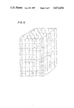
- FIG. 3 shows the configuration of a molecular controlled structure according to the invention.
- a first embodiment of this invention is described with reference to FIG. 1.
- a Si substrate 10 formed with SiO 2 there is formed by a chemical adsorption process, a monomolecular film 12 of ##STR1## through hydrolysis and dessication, and the reaction with the surface of a silane surface active agent, e.g., CH 2 ⁇ CH--(CH 2 ) n --SiCl 3 (n represents an integer, preferably being 10 ⁇ 20).
- a silane surface active agent e.g., CH 2 ⁇ CH--(CH 2 ) n --SiCl 3 (n represents an integer, preferably being 10 ⁇ 20).
- the treated substrate is dipped in a solution of this surfactant at its concentration of 2.0 ⁇ 10 -3 -5.0 ⁇ 10 31 2 mol/l in 80% n-hexane, 12% tetrachlorocarbon and 8% chloroform, to form a bonding 14 of ##STR2## at the SiO 2 surface [FIG. 1(a)].
- a silane surface active agent (CH 2 ⁇ CH--(CH 2 ) n --SiCl 3 ) 22 is added to active group portion which has an --OH group 20 by use of the similar technique to that above stated, so that a bonding 24 of ##STR3## is formed [FIG. 1(c)].
- a molecular film 26 of ##STR4## is selectively formed at a desired area. Further, on the surface of the molecules added, vinyl groups 28 are juxtaposed and form a film.
- a molecular controlled structure is produced in such a manner that molecules are juxtaposed regularly in a three dimensional direction.
- normal chain type hydrocarbons which have CH 2 ⁇ CH-- groups at one end of the molecules and have --SiCl 3 groups at the other end of molecules (silane surface active agent) are used. If functional groups, for example, diacetylene, pyrrole, chenylene, phenylene etc. are inserted between the --CH 2 --CH 2 -- bondings of normal chain type hydrocarbons or added instead of H, conjugated double bondings which show electric conductivity at the molecular level can be formed and it is possible to control the forming of wiring of organic molecules which are necessary for the production of molecular devices at the molecular level.
- functional groups for example, diacetylene, pyrrole, chenylene, phenylene etc.
- diacetylene group 30 is inserted between --CH 2 --CH 2 -- groups.
- a deep UV irradiation is effected so that molecular wiring of the poly-diacetylene 32 [FIG. 2(b)] can be formed in a direction which is desired in the same plane.
- molecules 34 including a phenyl group 36 instead of the abovestated diacetylene group can be added by the irradiation of electron beams 18 at the side position of the poly-diacetylene forming layer 40, whereby molecules having a phenyl group are regularly formed as a layer 42, in adjacent to the layer 40 of molecules having diacetylene group.
- cyanobromide (CNBr) is added to the --OH group 6 as shown in the following formula (3) to be thereby cyanized. ##STR5## Thereafter, an amino group is reacted therewith so that a monomolecule can be selectively added. [cyanobromide technique].
- the diameter of the electron beam is made smaller (e.g., about 5 ⁇ ), it becomes possible to produce a molecular controlled structure by controlling each molecule one by one.
- A, B, C represent different functional groups, respectively.
- the molecules having 3 kinds of functional groups are formed regularly in 3 (i.e., vertical, horizontal, hight) directions.
Abstract
Description
Claims (7)
Applications Claiming Priority (2)
| Application Number | Priority Date | Filing Date | Title |
|---|---|---|---|
| JP59216649A JPS6194042A (en) | 1984-10-16 | 1984-10-16 | Molecular construction and its manufacture |
| JP59-216649 | 1984-10-16 |
Publications (1)
| Publication Number | Publication Date |
|---|---|
| US4673474A true US4673474A (en) | 1987-06-16 |
Family
ID=16691752
Family Applications (1)
| Application Number | Title | Priority Date | Filing Date |
|---|---|---|---|
| US06/787,368 Expired - Lifetime US4673474A (en) | 1984-10-16 | 1985-10-15 | Molecular controlled structure and method of producing the same |
Country Status (4)
| Country | Link |
|---|---|
| US (1) | US4673474A (en) |
| EP (1) | EP0178606B1 (en) |
| JP (1) | JPS6194042A (en) |
| DE (1) | DE3585198D1 (en) |
Cited By (50)
| Publication number | Priority date | Publication date | Assignee | Title |
|---|---|---|---|---|
| US5035782A (en) * | 1988-06-28 | 1991-07-30 | Matsushita Electric Industrial Co., Ltd. | Method for the formation of monomolecular adsorption films or built-up films of monomolecular layers using silane compounds having an acetylene or diacetylene bond |
| US5196227A (en) * | 1988-08-05 | 1993-03-23 | Matsushita Electric Industrial Co., Ltd. | Method for making optical recording mediums |
| US5238746A (en) * | 1990-11-06 | 1993-08-24 | Matsushita Electric Industrial Co., Ltd. | Fluorocarbon-based polymer lamination coating film and method of manufacturing the same |
| US5240774A (en) * | 1990-10-25 | 1993-08-31 | Matsushita Electric Industrial Co., Ltd. | Fluorocarbon-based coating film and method of manufacturing the same |
| US5264731A (en) * | 1987-06-25 | 1993-11-23 | Matsushita Electric Industrial Co., Ltd. | Method for fabricating semiconductor device |
| US5372888A (en) * | 1991-02-06 | 1994-12-13 | Matsushita Electric Industrial Co., Ltd. | Chemically adsorbed film and method of manufacturing the same |
| US5380585A (en) * | 1990-10-25 | 1995-01-10 | Matsushita Electric Industrial Co., Ltd. | Chemically adsorbed monomolecular lamination film |
| US5474839A (en) * | 1991-03-14 | 1995-12-12 | Matsushita Electric Industrial Co., Ltd. | Surface-treated apparel material |
| US5652059A (en) * | 1991-11-20 | 1997-07-29 | Bar Ilan University | Method for attaching microspheres to a substrate |
| US5747158A (en) * | 1992-07-29 | 1998-05-05 | Matsushita Electric Industrial Co., Ltd. | Chemically adsorbed multilayer film |
| EP0511650B1 (en) * | 1991-04-30 | 1998-11-11 | Matsushita Electric Industrial Co., Ltd. | Antistatic film and method of manufacturing the same |
| US6099958A (en) * | 1992-07-29 | 2000-08-08 | Matsushita Electric Industrial Co., Ltd. | Lubricating film comprising a covalently bonded, chemically adsorbed film and a physically adsorbed organic compound formed thereon |
| USRE37698E1 (en) * | 1990-10-25 | 2002-05-14 | Matsushita Electric Industrial Co. | Method of manufacturing a fluorocarbon-based coating film |
| US20020117659A1 (en) * | 2000-12-11 | 2002-08-29 | Lieber Charles M. | Nanosensors |
| US6503567B2 (en) | 1990-12-25 | 2003-01-07 | Matsushita Electric Industrial Co., Ltd. | Transparent substrate and method of manufacturing the same |
| US6521334B1 (en) | 1990-12-25 | 2003-02-18 | Matsushita Electric Industrial Co., Ltd. | Transparent substrate and method of manufacturing the same |
| US6574130B2 (en) | 2001-07-25 | 2003-06-03 | Nantero, Inc. | Hybrid circuit having nanotube electromechanical memory |
| US20030199172A1 (en) * | 2001-07-25 | 2003-10-23 | Thomas Rueckes | Methods of nanotube films and articles |
| US6643165B2 (en) | 2001-07-25 | 2003-11-04 | Nantero, Inc. | Electromechanical memory having cell selection circuitry constructed with nanotube technology |
| US6706402B2 (en) | 2001-07-25 | 2004-03-16 | Nantero, Inc. | Nanotube films and articles |
| US6781166B2 (en) | 1999-07-02 | 2004-08-24 | President & Fellows Of Harvard College | Nanoscopic wire-based devices and arrays |
| US20040164289A1 (en) * | 2001-12-28 | 2004-08-26 | Nantero, Inc. | Electromechanical three-trace junction devices |
| US6784028B2 (en) | 2001-12-28 | 2004-08-31 | Nantero, Inc. | Methods of making electromechanical three-trace junction devices |
| US20040214366A1 (en) * | 2001-07-25 | 2004-10-28 | Nantero, Inc. | Electromechanical memory array using nanotube ribbons and method for making same |
| US20050129926A1 (en) * | 2003-12-12 | 2005-06-16 | Grant Kloster | Sealing porous dielectric materials |
| US6911682B2 (en) | 2001-12-28 | 2005-06-28 | Nantero, Inc. | Electromechanical three-trace junction devices |
| US20050164432A1 (en) * | 2000-08-22 | 2005-07-28 | President And Fellows Of Harvard College | Doped elongated semiconductors, growing such semiconductors, devices including such semiconductors and fabricating such devices |
| US20060175601A1 (en) * | 2000-08-22 | 2006-08-10 | President And Fellows Of Harvard College | Nanoscale wires and related devices |
| US7254151B2 (en) | 2002-07-19 | 2007-08-07 | President & Fellows Of Harvard College | Nanoscale coherent optical components |
| US7274078B2 (en) | 2001-07-25 | 2007-09-25 | Nantero, Inc. | Devices having vertically-disposed nanofabric articles and methods of making the same |
| US20070264623A1 (en) * | 2004-06-15 | 2007-11-15 | President And Fellows Of Harvard College | Nanosensors |
| US7301199B2 (en) | 2000-08-22 | 2007-11-27 | President And Fellows Of Harvard College | Nanoscale wires and related devices |
| US7304357B2 (en) | 2001-07-25 | 2007-12-04 | Nantero, Inc. | Devices having horizontally-disposed nanofabric articles and methods of making the same |
| US7335395B2 (en) | 2002-04-23 | 2008-02-26 | Nantero, Inc. | Methods of using pre-formed nanotubes to make carbon nanotube films, layers, fabrics, ribbons, elements and articles |
| US20080191196A1 (en) * | 2005-06-06 | 2008-08-14 | Wei Lu | Nanowire heterostructures |
| US20090004852A1 (en) * | 2004-02-13 | 2009-01-01 | President And Fellows Of Havard College | Nanostructures Containing Metal Semiconductor Compounds |
| US20090095950A1 (en) * | 2004-12-06 | 2009-04-16 | President And Fellows Of Harvard College | Nanoscale Wire-Based Data Storage |
| US20090124025A1 (en) * | 2003-06-03 | 2009-05-14 | Nanosys, Inc. | Nanowire-based sensor configurations |
| US7560136B2 (en) | 2003-01-13 | 2009-07-14 | Nantero, Inc. | Methods of using thin metal layers to make carbon nanotube films, layers, fabrics, ribbons, elements and articles |
| US7566478B2 (en) | 2001-07-25 | 2009-07-28 | Nantero, Inc. | Methods of making carbon nanotube films, layers, fabrics, ribbons, elements and articles |
| US20100087013A1 (en) * | 2006-06-12 | 2010-04-08 | President And Fellows Of Harvard College | Nanosensors and related technologies |
| US20100152057A1 (en) * | 2006-11-22 | 2010-06-17 | President And Fellows Of Havard College | High-sensitivity nanoscale wire sensors |
| US20100227382A1 (en) * | 2005-05-25 | 2010-09-09 | President And Fellows Of Harvard College | Nanoscale sensors |
| US20110151263A1 (en) * | 2009-11-10 | 2011-06-23 | Linford Matthew R | Multilayer growth by gas phase deposition |
| US7968474B2 (en) | 2006-11-09 | 2011-06-28 | Nanosys, Inc. | Methods for nanowire alignment and deposition |
| US20110165337A1 (en) * | 2007-05-07 | 2011-07-07 | Nanosys, Inc. | Method and system for printing aligned nanowires and other electrical devices |
| US8058640B2 (en) | 2006-09-11 | 2011-11-15 | President And Fellows Of Harvard College | Branched nanoscale wires |
| US9297796B2 (en) | 2009-09-24 | 2016-03-29 | President And Fellows Of Harvard College | Bent nanowires and related probing of species |
| US9390951B2 (en) | 2009-05-26 | 2016-07-12 | Sharp Kabushiki Kaisha | Methods and systems for electric field deposition of nanowires and other devices |
| US11377740B2 (en) | 2015-09-11 | 2022-07-05 | Fei Company | Nanofabrication using a new class of electron beam induced surface processing techniques |
Families Citing this family (12)
| Publication number | Priority date | Publication date | Assignee | Title |
|---|---|---|---|---|
| JPS6221151A (en) * | 1985-07-19 | 1987-01-29 | Matsushita Electric Ind Co Ltd | Formation of pattern |
| JPS62293242A (en) * | 1986-06-12 | 1987-12-19 | Matsushita Electric Ind Co Ltd | Method and material for forming pattern |
| JPS6396655A (en) * | 1986-10-14 | 1988-04-27 | Matsushita Electric Ind Co Ltd | Pattern forming method |
| JPS63237293A (en) * | 1987-03-24 | 1988-10-03 | Matsushita Electric Ind Co Ltd | Modulatable molecular element |
| JPH0774894B2 (en) * | 1987-05-25 | 1995-08-09 | コニカ株式会社 | Silver halide photographic light-sensitive material with improved sharpness |
| DE3723540A1 (en) * | 1987-07-16 | 1989-01-26 | Basf Ag | METHOD FOR MODIFYING AND ADDRESSING ORGANIC FILMS IN THE MOLECULAR AREA |
| US4968524A (en) * | 1987-10-16 | 1990-11-06 | Matsushita Electric Industrial Co., Ltd. | Process for producing a polyacetylene |
| JPH07103190B2 (en) * | 1989-02-15 | 1995-11-08 | 松下電器産業株式会社 | Organic conductive thin film and manufacturing method thereof |
| US5260115A (en) * | 1989-02-15 | 1993-11-09 | Matsushita Electric Industrial Co., Ltd. | Organic electro-conductive thin films and process for production thereof |
| JP2500824B2 (en) * | 1990-10-25 | 1996-05-29 | 松下電器産業株式会社 | Fluorocarbon coating film and method for producing the same |
| JP2622316B2 (en) * | 1991-06-04 | 1997-06-18 | 松下電器産業株式会社 | Water / oil repellent film and method for producing the same |
| JP2009158691A (en) * | 2007-12-26 | 2009-07-16 | Sharp Corp | Organic device and manufacturing method thereof |
Citations (5)
| Publication number | Priority date | Publication date | Assignee | Title |
|---|---|---|---|---|
| US2959569A (en) * | 1956-07-05 | 1960-11-08 | Dow Corning | Method of preparing organosilicon graft polymers |
| US3305524A (en) * | 1962-11-27 | 1967-02-21 | Gen Electric | Polysiloxanes |
| US3573334A (en) * | 1964-04-02 | 1971-03-30 | Union Carbide Corp | Olefinic silicone-organic polymer graft copolymers |
| US4188273A (en) * | 1973-11-22 | 1980-02-12 | Sumitomo Chemical Company, Limited | Process for preparing novel thin films |
| US4597999A (en) * | 1984-10-04 | 1986-07-01 | The Hospital For Sick Children | Method for coupling a hydrocarbon containing molecular species |
Family Cites Families (5)
| Publication number | Priority date | Publication date | Assignee | Title |
|---|---|---|---|---|
| JPS6056285B2 (en) * | 1977-04-28 | 1985-12-09 | 凸版印刷株式会社 | How to create a resist film |
| JPS5642229A (en) * | 1979-06-25 | 1981-04-20 | University Patents Inc | New photooresist composition |
| JPS58111029A (en) * | 1981-12-24 | 1983-07-01 | Kureha Chem Ind Co Ltd | Manufacture of built-up film of diacetylene compound |
| JPS58112078A (en) * | 1981-12-26 | 1983-07-04 | Daikin Ind Ltd | Method of forming film of fluoroalkyl acrylate polymer on surface of base body |
| JPS59148335A (en) * | 1983-02-14 | 1984-08-25 | Nippon Telegr & Teleph Corp <Ntt> | Forming method of minute pattern |
-
1984
- 1984-10-16 JP JP59216649A patent/JPS6194042A/en not_active Expired - Lifetime
-
1985
- 1985-10-11 DE DE8585112928T patent/DE3585198D1/en not_active Expired - Lifetime
- 1985-10-11 EP EP85112928A patent/EP0178606B1/en not_active Expired
- 1985-10-15 US US06/787,368 patent/US4673474A/en not_active Expired - Lifetime
Patent Citations (5)
| Publication number | Priority date | Publication date | Assignee | Title |
|---|---|---|---|---|
| US2959569A (en) * | 1956-07-05 | 1960-11-08 | Dow Corning | Method of preparing organosilicon graft polymers |
| US3305524A (en) * | 1962-11-27 | 1967-02-21 | Gen Electric | Polysiloxanes |
| US3573334A (en) * | 1964-04-02 | 1971-03-30 | Union Carbide Corp | Olefinic silicone-organic polymer graft copolymers |
| US4188273A (en) * | 1973-11-22 | 1980-02-12 | Sumitomo Chemical Company, Limited | Process for preparing novel thin films |
| US4597999A (en) * | 1984-10-04 | 1986-07-01 | The Hospital For Sick Children | Method for coupling a hydrocarbon containing molecular species |
Non-Patent Citations (8)
| Title |
|---|
| Anthony DiBenedetto et al., "Characterization of S-Glass/Polymer Interfaces Using Ion Scattering Spectroscopy and Scattered Ion Mass Spectroscopy", Journal of Colloid and Interface Science, vol. 64, No. 3, May 1978, pp. 480-500. |
| Anthony DiBenedetto et al., Characterization of S Glass/Polymer Interfaces Using Ion Scattering Spectroscopy and Scattered Ion Mass Spectroscopy , Journal of Colloid and Interface Science, vol. 64, No. 3, May 1978, pp. 480 500. * |
| Hatsuo Ishida et al., "Molecular Organization of the Coupling Agent Interphase of Fiber-Glass Reinforced Plastics", Journal of Polymer Science, Polymer Physics Edition, vol. 17, 1807-1813, (1979), pp. 1806-1813. |
| Hatsuo Ishida et al., Molecular Organization of the Coupling Agent Interphase of Fiber Glass Reinforced Plastics , Journal of Polymer Science, Polymer Physics Edition, vol. 17, 1807 1813, (1979), pp. 1806 1813. * |
| Netzer et al, J. Amer. Chem. Soc., (1983), vol. 105, pp. 674 676. * |
| Netzer et al, J. Amer. Chem. Soc., (1983), vol. 105, pp. 674-676. |
| Yoshio Okahata et al., "A Large Nylon Capsule Coated with a Synthetic Bilayer Membrane. Permeability Control of NaCl by Phase Transition of the Dialkylammonium Bilayer Coating", Journal of the Americal Chemical Society, vol. 105, No. 15, Jul. 27, 1983. |
| Yoshio Okahata et al., A Large Nylon Capsule Coated with a Synthetic Bilayer Membrane. Permeability Control of NaCl by Phase Transition of the Dialkylammonium Bilayer Coating , Journal of the Americal Chemical Society, vol. 105, No. 15, Jul. 27, 1983. * |
Cited By (125)
| Publication number | Priority date | Publication date | Assignee | Title |
|---|---|---|---|---|
| US5264731A (en) * | 1987-06-25 | 1993-11-23 | Matsushita Electric Industrial Co., Ltd. | Method for fabricating semiconductor device |
| US5035782A (en) * | 1988-06-28 | 1991-07-30 | Matsushita Electric Industrial Co., Ltd. | Method for the formation of monomolecular adsorption films or built-up films of monomolecular layers using silane compounds having an acetylene or diacetylene bond |
| US5196227A (en) * | 1988-08-05 | 1993-03-23 | Matsushita Electric Industrial Co., Ltd. | Method for making optical recording mediums |
| US5324548A (en) * | 1988-08-05 | 1994-06-28 | Matsushita Electric Industrial Co., Ltd. | Method for making optical recording mediums |
| USRE37698E1 (en) * | 1990-10-25 | 2002-05-14 | Matsushita Electric Industrial Co. | Method of manufacturing a fluorocarbon-based coating film |
| US5538762A (en) * | 1990-10-25 | 1996-07-23 | Matsushita Electric Industrial Co., Ltd. | Method of manufacturing a fluorocarbon-based coating film |
| USRE38752E1 (en) * | 1990-10-25 | 2005-07-05 | Matsushita Electric Industrial Co., Ltd | Method of manufacturing a fluorocarbon-based coating film |
| US5380585A (en) * | 1990-10-25 | 1995-01-10 | Matsushita Electric Industrial Co., Ltd. | Chemically adsorbed monomolecular lamination film |
| US5466486A (en) * | 1990-10-25 | 1995-11-14 | Matsushita Electric Industrial Co., Ltd. | Chemically adsorbed monomolecular lamination film |
| USRE39045E1 (en) * | 1990-10-25 | 2006-03-28 | Matsushita Electric Industrial Co., Ltd. | Method of manufacturing a fluorocarbon-based coating film |
| US5240774A (en) * | 1990-10-25 | 1993-08-31 | Matsushita Electric Industrial Co., Ltd. | Fluorocarbon-based coating film and method of manufacturing the same |
| US5238746A (en) * | 1990-11-06 | 1993-08-24 | Matsushita Electric Industrial Co., Ltd. | Fluorocarbon-based polymer lamination coating film and method of manufacturing the same |
| US6503567B2 (en) | 1990-12-25 | 2003-01-07 | Matsushita Electric Industrial Co., Ltd. | Transparent substrate and method of manufacturing the same |
| US6521334B1 (en) | 1990-12-25 | 2003-02-18 | Matsushita Electric Industrial Co., Ltd. | Transparent substrate and method of manufacturing the same |
| US5500250A (en) * | 1991-02-06 | 1996-03-19 | Matsushita Electric Industrial Co., Ltd. | Chemically adsorbed film and method of manufacturing the same |
| US5372888A (en) * | 1991-02-06 | 1994-12-13 | Matsushita Electric Industrial Co., Ltd. | Chemically adsorbed film and method of manufacturing the same |
| US5474839A (en) * | 1991-03-14 | 1995-12-12 | Matsushita Electric Industrial Co., Ltd. | Surface-treated apparel material |
| EP0511650B1 (en) * | 1991-04-30 | 1998-11-11 | Matsushita Electric Industrial Co., Ltd. | Antistatic film and method of manufacturing the same |
| US5652059A (en) * | 1991-11-20 | 1997-07-29 | Bar Ilan University | Method for attaching microspheres to a substrate |
| US6099958A (en) * | 1992-07-29 | 2000-08-08 | Matsushita Electric Industrial Co., Ltd. | Lubricating film comprising a covalently bonded, chemically adsorbed film and a physically adsorbed organic compound formed thereon |
| US5747158A (en) * | 1992-07-29 | 1998-05-05 | Matsushita Electric Industrial Co., Ltd. | Chemically adsorbed multilayer film |
| US20080116491A1 (en) * | 1999-07-02 | 2008-05-22 | President And Fellows Of Harvard College | Nanoscopic wire-based devices and arrays |
| US7172953B2 (en) | 1999-07-02 | 2007-02-06 | President And Fellows Of Harvard College | Methods of forming nanoscopic wire-based devices and arrays |
| US20070161237A1 (en) * | 1999-07-02 | 2007-07-12 | President And Fellows Of Harvard College | Nanoscopic wired-based devices and arrays |
| US20110174619A1 (en) * | 1999-07-02 | 2011-07-21 | President And Fellows Of Harvard College | Nonoscopic wired-based devices and arrays |
| US20070045667A1 (en) * | 1999-07-02 | 2007-03-01 | President And Fellows Of Harvard College | Nanoscopic wired-based devices and arrays |
| US6781166B2 (en) | 1999-07-02 | 2004-08-24 | President & Fellows Of Harvard College | Nanoscopic wire-based devices and arrays |
| US20070272951A1 (en) * | 1999-07-02 | 2007-11-29 | President And Fellows Of Harvard College | Nanoscopic wire-based devices and arrays |
| US8178907B2 (en) | 1999-07-02 | 2012-05-15 | President And Fellows Of Harvard College | Nanoscopic wire-based electrical crossbar memory-devices and arrays |
| US20040188721A1 (en) * | 1999-07-02 | 2004-09-30 | President And Fellows Of Harvard University | Nanoscopic wired-based devices and arrays |
| US20060237749A1 (en) * | 1999-07-02 | 2006-10-26 | President And Fellows Of Harvard College | Nanoscopic wire-based devices and arrays |
| US20060220067A1 (en) * | 1999-07-02 | 2006-10-05 | President And Fellows Of Harvard College | Nanoscopic wire-based devices and arrays |
| US7399691B2 (en) | 1999-07-02 | 2008-07-15 | President And Fellows Of Harvard College | Methods of forming nanoscopic wire-based devices and arrays |
| US8471298B2 (en) | 1999-07-02 | 2013-06-25 | President And Fellows Of Harvard College | Nanoscopic wire-based devices and arrays |
| US20050117441A1 (en) * | 1999-07-02 | 2005-06-02 | President And Fellows Of Harvard College | Nanoscopic wire-based devices and arrays |
| US7666708B2 (en) | 2000-08-22 | 2010-02-23 | President And Fellows Of Harvard College | Doped elongated semiconductors, growing such semiconductors, devices including such semiconductors, and fabricating such devices |
| US7301199B2 (en) | 2000-08-22 | 2007-11-27 | President And Fellows Of Harvard College | Nanoscale wires and related devices |
| US8153470B2 (en) | 2000-08-22 | 2012-04-10 | President And Fellows Of Harvard College | Doped elongated semiconductors, growing such semiconductors, devices including such semiconductors, and fabricating such devices |
| US20090057650A1 (en) * | 2000-08-22 | 2009-03-05 | President And Fellows Of Harvard College | Nanoscale wires and related devices |
| US20050164432A1 (en) * | 2000-08-22 | 2005-07-28 | President And Fellows Of Harvard College | Doped elongated semiconductors, growing such semiconductors, devices including such semiconductors and fabricating such devices |
| US7476596B2 (en) | 2000-08-22 | 2009-01-13 | President And Fellows Of Harvard College | Doped elongated semiconductors, growing such semiconductors, devices including such semiconductors, and fabricating such devices |
| US7211464B2 (en) | 2000-08-22 | 2007-05-01 | President & Fellows Of Harvard College | Doped elongated semiconductors, growing such semiconductors, devices including such semiconductors and fabricating such devices |
| US20070048492A1 (en) * | 2000-08-22 | 2007-03-01 | President And Fellows Of Harvard College | Doped elongated semiconductors, growing such semiconductors, devices including such semiconductors, and fabricating such devices |
| US7595260B2 (en) | 2000-08-22 | 2009-09-29 | President And Fellows Of Harvard College | Doped elongated semiconductors, growing such semiconductors, devices including such semiconductors, and fabricating such devices |
| US20070032052A1 (en) * | 2000-08-22 | 2007-02-08 | President And Fellows Of Harvard College | Doped elongated semiconductors, growing such semiconductors, devices including such semiconductors, and fabricating such devices |
| US20060175601A1 (en) * | 2000-08-22 | 2006-08-10 | President And Fellows Of Harvard College | Nanoscale wires and related devices |
| US20100093158A1 (en) * | 2000-08-22 | 2010-04-15 | President And Fellows Of Harvard College | Doped elongated semiconductors, growing such semiconductors, devices including such semiconductors and fabricating such devices |
| US7915151B2 (en) | 2000-08-22 | 2011-03-29 | President And Fellows Of Harvard College | Doped elongated semiconductors, growing such semiconductors, devices including such semiconductors and fabricating such devices |
| US20100155698A1 (en) * | 2000-08-22 | 2010-06-24 | President And Fellows Of Harvard College | Nanoscale wires and related devices |
| US20070032023A1 (en) * | 2000-08-22 | 2007-02-08 | President And Fellows Of Harvard College | Doped elongated semiconductors, growing such semiconductors, devices including such semiconductors, and fabricating such devices |
| US20070026645A1 (en) * | 2000-08-22 | 2007-02-01 | President And Fellows Of Harvard College | Doped elongated semiconductors, growing such semiconductors, devices including such semiconductors, and fabricating such devices |
| US20070032051A1 (en) * | 2000-08-22 | 2007-02-08 | President And Fellows Of Harvard College | Doped elongated semiconductors, growing such semiconductors, devices including such semiconductors, and fabricating such devices |
| US20100022012A1 (en) * | 2000-12-11 | 2010-01-28 | President And Fellows Of Harvard College | Nanosensors |
| US7911009B2 (en) | 2000-12-11 | 2011-03-22 | President And Fellows Of Harvard College | Nanosensors |
| US7129554B2 (en) | 2000-12-11 | 2006-10-31 | President & Fellows Of Harvard College | Nanosensors |
| US7385267B2 (en) | 2000-12-11 | 2008-06-10 | President And Fellows Of Harvard College | Nanosensors |
| US20060054936A1 (en) * | 2000-12-11 | 2006-03-16 | President And Fellows Of Harvard College | Nanosensors |
| US7956427B2 (en) | 2000-12-11 | 2011-06-07 | President And Fellows Of Harvard College | Nanosensors |
| US20080211040A1 (en) * | 2000-12-11 | 2008-09-04 | President And Fellows Of Harvard College | Nanosensors |
| US20070158766A1 (en) * | 2000-12-11 | 2007-07-12 | President And Fellows Of Harvard College | Nanosensors |
| US7619290B2 (en) | 2000-12-11 | 2009-11-17 | President And Fellows Of Harvard College | Nanosensors |
| US8399339B2 (en) | 2000-12-11 | 2013-03-19 | President And Fellows Of Harvard College | Nanosensors |
| US7256466B2 (en) | 2000-12-11 | 2007-08-14 | President & Fellows Of Harvard College | Nanosensors |
| US20020117659A1 (en) * | 2000-12-11 | 2002-08-29 | Lieber Charles M. | Nanosensors |
| US7264990B2 (en) | 2001-07-25 | 2007-09-04 | Nantero, Inc. | Methods of nanotubes films and articles |
| US7745810B2 (en) | 2001-07-25 | 2010-06-29 | Nantero, Inc. | Nanotube films and articles |
| US7298016B2 (en) | 2001-07-25 | 2007-11-20 | Nantero, Inc. | Electromechanical memory array using nanotube ribbons and method for making same |
| US7274078B2 (en) | 2001-07-25 | 2007-09-25 | Nantero, Inc. | Devices having vertically-disposed nanofabric articles and methods of making the same |
| US6574130B2 (en) | 2001-07-25 | 2003-06-03 | Nantero, Inc. | Hybrid circuit having nanotube electromechanical memory |
| US7304357B2 (en) | 2001-07-25 | 2007-12-04 | Nantero, Inc. | Devices having horizontally-disposed nanofabric articles and methods of making the same |
| US20030165074A1 (en) * | 2001-07-25 | 2003-09-04 | Nantero, Inc. | Hybrid circuit having nanotube electromechanical memory |
| US7335528B2 (en) | 2001-07-25 | 2008-02-26 | Nantero, Inc. | Methods of nanotube films and articles |
| US7342818B2 (en) | 2001-07-25 | 2008-03-11 | Nantero, Inc. | Hybrid circuit having nanotube electromechanical memory |
| US20030199172A1 (en) * | 2001-07-25 | 2003-10-23 | Thomas Rueckes | Methods of nanotube films and articles |
| US7120047B2 (en) | 2001-07-25 | 2006-10-10 | Segal Brent M | Device selection circuitry constructed with nanotube technology |
| US7056758B2 (en) | 2001-07-25 | 2006-06-06 | Nantero, Inc. | Electromechanical memory array using nanotube ribbons and method for making same |
| US6643165B2 (en) | 2001-07-25 | 2003-11-04 | Nantero, Inc. | Electromechanical memory having cell selection circuitry constructed with nanotube technology |
| US8101976B2 (en) | 2001-07-25 | 2012-01-24 | Nantero Inc. | Device selection circuitry constructed with nanotube ribbon technology |
| US6706402B2 (en) | 2001-07-25 | 2004-03-16 | Nantero, Inc. | Nanotube films and articles |
| US6942921B2 (en) | 2001-07-25 | 2005-09-13 | Nantero, Inc. | Nanotube films and articles |
| US6919592B2 (en) | 2001-07-25 | 2005-07-19 | Nantero, Inc. | Electromechanical memory array using nanotube ribbons and method for making same |
| US20040085805A1 (en) * | 2001-07-25 | 2004-05-06 | Nantero, Inc. | Device selection circuitry constructed with nanotube technology |
| US20040214366A1 (en) * | 2001-07-25 | 2004-10-28 | Nantero, Inc. | Electromechanical memory array using nanotube ribbons and method for making same |
| US6836424B2 (en) | 2001-07-25 | 2004-12-28 | Nantero, Inc. | Hybrid circuit having nanotube electromechanical memory |
| US6835591B2 (en) | 2001-07-25 | 2004-12-28 | Nantero, Inc. | Methods of nanotube films and articles |
| US7566478B2 (en) | 2001-07-25 | 2009-07-28 | Nantero, Inc. | Methods of making carbon nanotube films, layers, fabrics, ribbons, elements and articles |
| US20050063210A1 (en) * | 2001-07-25 | 2005-03-24 | Nantero, Inc. | Hybrid circuit having nanotube electromechanical memory |
| US6784028B2 (en) | 2001-12-28 | 2004-08-31 | Nantero, Inc. | Methods of making electromechanical three-trace junction devices |
| US7176505B2 (en) | 2001-12-28 | 2007-02-13 | Nantero, Inc. | Electromechanical three-trace junction devices |
| US6979590B2 (en) | 2001-12-28 | 2005-12-27 | Nantero, Inc. | Methods of making electromechanical three-trace junction devices |
| US6911682B2 (en) | 2001-12-28 | 2005-06-28 | Nantero, Inc. | Electromechanical three-trace junction devices |
| US20040164289A1 (en) * | 2001-12-28 | 2004-08-26 | Nantero, Inc. | Electromechanical three-trace junction devices |
| US7521736B2 (en) | 2001-12-28 | 2009-04-21 | Nantero, Inc. | Electromechanical three-trace junction devices |
| US7915066B2 (en) | 2001-12-28 | 2011-03-29 | Nantero, Inc. | Methods of making electromechanical three-trace junction devices |
| US7335395B2 (en) | 2002-04-23 | 2008-02-26 | Nantero, Inc. | Methods of using pre-formed nanotubes to make carbon nanotube films, layers, fabrics, ribbons, elements and articles |
| US7254151B2 (en) | 2002-07-19 | 2007-08-07 | President & Fellows Of Harvard College | Nanoscale coherent optical components |
| US7560136B2 (en) | 2003-01-13 | 2009-07-14 | Nantero, Inc. | Methods of using thin metal layers to make carbon nanotube films, layers, fabrics, ribbons, elements and articles |
| US20090124025A1 (en) * | 2003-06-03 | 2009-05-14 | Nanosys, Inc. | Nanowire-based sensor configurations |
| US7910064B2 (en) | 2003-06-03 | 2011-03-22 | Nanosys, Inc. | Nanowire-based sensor configurations |
| US20050129926A1 (en) * | 2003-12-12 | 2005-06-16 | Grant Kloster | Sealing porous dielectric materials |
| US7658975B2 (en) * | 2003-12-12 | 2010-02-09 | Intel Corporation | Sealing porous dielectric materials |
| US20090227107A9 (en) * | 2004-02-13 | 2009-09-10 | President And Fellows Of Havard College | Nanostructures Containing Metal Semiconductor Compounds |
| US20090004852A1 (en) * | 2004-02-13 | 2009-01-01 | President And Fellows Of Havard College | Nanostructures Containing Metal Semiconductor Compounds |
| US20070264623A1 (en) * | 2004-06-15 | 2007-11-15 | President And Fellows Of Harvard College | Nanosensors |
| US20090095950A1 (en) * | 2004-12-06 | 2009-04-16 | President And Fellows Of Harvard College | Nanoscale Wire-Based Data Storage |
| US8154002B2 (en) | 2004-12-06 | 2012-04-10 | President And Fellows Of Harvard College | Nanoscale wire-based data storage |
| US20100227382A1 (en) * | 2005-05-25 | 2010-09-09 | President And Fellows Of Harvard College | Nanoscale sensors |
| US8232584B2 (en) | 2005-05-25 | 2012-07-31 | President And Fellows Of Harvard College | Nanoscale sensors |
| US20080191196A1 (en) * | 2005-06-06 | 2008-08-14 | Wei Lu | Nanowire heterostructures |
| US7858965B2 (en) | 2005-06-06 | 2010-12-28 | President And Fellows Of Harvard College | Nanowire heterostructures |
| US20100087013A1 (en) * | 2006-06-12 | 2010-04-08 | President And Fellows Of Harvard College | Nanosensors and related technologies |
| US9102521B2 (en) | 2006-06-12 | 2015-08-11 | President And Fellows Of Harvard College | Nanosensors and related technologies |
| US9903862B2 (en) | 2006-06-12 | 2018-02-27 | President And Fellows Of Harvard College | Nanosensors and related technologies |
| US8058640B2 (en) | 2006-09-11 | 2011-11-15 | President And Fellows Of Harvard College | Branched nanoscale wires |
| US7968474B2 (en) | 2006-11-09 | 2011-06-28 | Nanosys, Inc. | Methods for nanowire alignment and deposition |
| US8252164B2 (en) | 2006-11-09 | 2012-08-28 | Nanosys, Inc. | Methods for nanowire alignment and deposition |
| US8575663B2 (en) | 2006-11-22 | 2013-11-05 | President And Fellows Of Harvard College | High-sensitivity nanoscale wire sensors |
| US9535063B2 (en) | 2006-11-22 | 2017-01-03 | President And Fellows Of Harvard College | High-sensitivity nanoscale wire sensors |
| US20100152057A1 (en) * | 2006-11-22 | 2010-06-17 | President And Fellows Of Havard College | High-sensitivity nanoscale wire sensors |
| US20110165337A1 (en) * | 2007-05-07 | 2011-07-07 | Nanosys, Inc. | Method and system for printing aligned nanowires and other electrical devices |
| US9390951B2 (en) | 2009-05-26 | 2016-07-12 | Sharp Kabushiki Kaisha | Methods and systems for electric field deposition of nanowires and other devices |
| US9297796B2 (en) | 2009-09-24 | 2016-03-29 | President And Fellows Of Harvard College | Bent nanowires and related probing of species |
| CN102695817A (en) * | 2009-11-10 | 2012-09-26 | 布莱阿姆青年大学 | Multilayer growth by gas phase deposition |
| US20110151263A1 (en) * | 2009-11-10 | 2011-06-23 | Linford Matthew R | Multilayer growth by gas phase deposition |
| US11377740B2 (en) | 2015-09-11 | 2022-07-05 | Fei Company | Nanofabrication using a new class of electron beam induced surface processing techniques |
Also Published As
| Publication number | Publication date |
|---|---|
| EP0178606B1 (en) | 1992-01-15 |
| EP0178606A3 (en) | 1987-09-02 |
| DE3585198D1 (en) | 1992-02-27 |
| EP0178606A2 (en) | 1986-04-23 |
| JPS6194042A (en) | 1986-05-12 |
Similar Documents
| Publication | Publication Date | Title |
|---|---|---|
| US4673474A (en) | Molecular controlled structure and method of producing the same | |
| US5017975A (en) | Organic electronic device with a monomolecular layer or multi-monomolecular layer having electroconductive conjugated bonds | |
| US5057339A (en) | Metallized polyacetylene-type or polyacene-type ultralong conjugated polymers and process for producing the same | |
| Bertilsson et al. | Infrared study of thiol monolayer assemblies on gold: preparation, characterization, and functionalization of mixed monolayers | |
| US4560599A (en) | Assembling multilayers of polymerizable surfactant on a surface of a solid material | |
| US5011518A (en) | Permselective membrane and process for producing the same | |
| US5102798A (en) | Surface functionalized Langmuir-Blodgett films for immobilization of active moieties | |
| EP1551066A1 (en) | Material with pattern surface for use as template and process for producing the same | |
| US4908299A (en) | Pattern forming method | |
| EP1016458A3 (en) | Photocatalyst comprising organic-inorganic hybrid materials, and processes for preparing the same | |
| CN100377795C (en) | Conjugated molecular assembly, method of fabricating the assembly and device including the assembly | |
| US5093154A (en) | Process for preparing a monomolecular built-up film | |
| US5681442A (en) | Method of producing an organic device | |
| Che et al. | Molecular recognition based on (3-mercaptopropyl) trimethoxysilane modified gold electrodes | |
| US5536982A (en) | Ultra thin polymer film electret | |
| US4996075A (en) | Method for producing ultrathin metal film and ultrathin-thin metal pattern | |
| US5277980A (en) | Mass of fine particles of inorganic material and a film of the fine inorganic particles | |
| US4968524A (en) | Process for producing a polyacetylene | |
| Mao et al. | Polymer immobilization to alkylchlorosilane organic monolayer films using sequential derivatization reactions | |
| US5019303A (en) | Process for producing polyacetylene | |
| US5304582A (en) | Process for producing polyacetylene or polyacene type long conjugated polymers | |
| US5304583A (en) | Process for producing polyacetylene or polyacene type long conjugated polymers | |
| US5248526A (en) | Process for producing polyacetylene or polyacene type long conjugated polymers | |
| JPH0290679A (en) | Very thin metal film and manufacture thereof | |
| US5302416A (en) | Process for producing polyacetylene or polyacene type long conjugated polymers |
Legal Events
| Date | Code | Title | Description |
|---|---|---|---|
| AS | Assignment |
Owner name: MATSUSHITA ELECTRIC INDUSTRIAL CO., LTD., 1006, OA Free format text: ASSIGNMENT OF ASSIGNORS INTEREST.;ASSIGNOR:OGAWA, KAZUFUMI;REEL/FRAME:004470/0320 Effective date: 19851004 |
|
| STCF | Information on status: patent grant |
Free format text: PATENTED CASE |
|
| FEPP | Fee payment procedure |
Free format text: PAYOR NUMBER ASSIGNED (ORIGINAL EVENT CODE: ASPN); ENTITY STATUS OF PATENT OWNER: LARGE ENTITY |
|
| FPAY | Fee payment |
Year of fee payment: 4 |
|
| FEPP | Fee payment procedure |
Free format text: PAYER NUMBER DE-ASSIGNED (ORIGINAL EVENT CODE: RMPN); ENTITY STATUS OF PATENT OWNER: LARGE ENTITY Free format text: PAYOR NUMBER ASSIGNED (ORIGINAL EVENT CODE: ASPN); ENTITY STATUS OF PATENT OWNER: LARGE ENTITY |
|
| FPAY | Fee payment |
Year of fee payment: 8 |
|
| FPAY | Fee payment |
Year of fee payment: 12 |