US5886414A - Removal of extended bond pads using intermetallics - Google Patents
Removal of extended bond pads using intermetallics Download PDFInfo
- Publication number
- US5886414A US5886414A US08/717,411 US71741196A US5886414A US 5886414 A US5886414 A US 5886414A US 71741196 A US71741196 A US 71741196A US 5886414 A US5886414 A US 5886414A
- Authority
- US
- United States
- Prior art keywords
- metal
- extension area
- wire bond
- area
- bond pad
- Prior art date
- Legal status (The legal status is an assumption and is not a legal conclusion. Google has not performed a legal analysis and makes no representation as to the accuracy of the status listed.)
- Expired - Lifetime
Links
Images


Classifications
-
- H—ELECTRICITY
- H01—ELECTRIC ELEMENTS
- H01L—SEMICONDUCTOR DEVICES NOT COVERED BY CLASS H10
- H01L22/00—Testing or measuring during manufacture or treatment; Reliability measurements, i.e. testing of parts without further processing to modify the parts as such; Structural arrangements therefor
- H01L22/30—Structural arrangements specially adapted for testing or measuring during manufacture or treatment, or specially adapted for reliability measurements
- H01L22/32—Additional lead-in metallisation on a device or substrate, e.g. additional pads or pad portions, lines in the scribe line, sacrificed conductors
-
- H—ELECTRICITY
- H01—ELECTRIC ELEMENTS
- H01L—SEMICONDUCTOR DEVICES NOT COVERED BY CLASS H10
- H01L24/00—Arrangements for connecting or disconnecting semiconductor or solid-state bodies; Methods or apparatus related thereto
- H01L24/01—Means for bonding being attached to, or being formed on, the surface to be connected, e.g. chip-to-package, die-attach, "first-level" interconnects; Manufacturing methods related thereto
- H01L24/02—Bonding areas ; Manufacturing methods related thereto
- H01L24/04—Structure, shape, material or disposition of the bonding areas prior to the connecting process
- H01L24/05—Structure, shape, material or disposition of the bonding areas prior to the connecting process of an individual bonding area
-
- H—ELECTRICITY
- H01—ELECTRIC ELEMENTS
- H01L—SEMICONDUCTOR DEVICES NOT COVERED BY CLASS H10
- H01L2224/00—Indexing scheme for arrangements for connecting or disconnecting semiconductor or solid-state bodies and methods related thereto as covered by H01L24/00
- H01L2224/01—Means for bonding being attached to, or being formed on, the surface to be connected, e.g. chip-to-package, die-attach, "first-level" interconnects; Manufacturing methods related thereto
- H01L2224/02—Bonding areas; Manufacturing methods related thereto
- H01L2224/0212—Auxiliary members for bonding areas, e.g. spacers
- H01L2224/02122—Auxiliary members for bonding areas, e.g. spacers being formed on the semiconductor or solid-state body
-
- H—ELECTRICITY
- H01—ELECTRIC ELEMENTS
- H01L—SEMICONDUCTOR DEVICES NOT COVERED BY CLASS H10
- H01L2224/00—Indexing scheme for arrangements for connecting or disconnecting semiconductor or solid-state bodies and methods related thereto as covered by H01L24/00
- H01L2224/01—Means for bonding being attached to, or being formed on, the surface to be connected, e.g. chip-to-package, die-attach, "first-level" interconnects; Manufacturing methods related thereto
- H01L2224/02—Bonding areas; Manufacturing methods related thereto
- H01L2224/04—Structure, shape, material or disposition of the bonding areas prior to the connecting process
- H01L2224/0401—Bonding areas specifically adapted for bump connectors, e.g. under bump metallisation [UBM]
-
- H—ELECTRICITY
- H01—ELECTRIC ELEMENTS
- H01L—SEMICONDUCTOR DEVICES NOT COVERED BY CLASS H10
- H01L2224/00—Indexing scheme for arrangements for connecting or disconnecting semiconductor or solid-state bodies and methods related thereto as covered by H01L24/00
- H01L2224/01—Means for bonding being attached to, or being formed on, the surface to be connected, e.g. chip-to-package, die-attach, "first-level" interconnects; Manufacturing methods related thereto
- H01L2224/02—Bonding areas; Manufacturing methods related thereto
- H01L2224/04—Structure, shape, material or disposition of the bonding areas prior to the connecting process
- H01L2224/04042—Bonding areas specifically adapted for wire connectors, e.g. wirebond pads
-
- H—ELECTRICITY
- H01—ELECTRIC ELEMENTS
- H01L—SEMICONDUCTOR DEVICES NOT COVERED BY CLASS H10
- H01L2224/00—Indexing scheme for arrangements for connecting or disconnecting semiconductor or solid-state bodies and methods related thereto as covered by H01L24/00
- H01L2224/01—Means for bonding being attached to, or being formed on, the surface to be connected, e.g. chip-to-package, die-attach, "first-level" interconnects; Manufacturing methods related thereto
- H01L2224/02—Bonding areas; Manufacturing methods related thereto
- H01L2224/04—Structure, shape, material or disposition of the bonding areas prior to the connecting process
- H01L2224/05—Structure, shape, material or disposition of the bonding areas prior to the connecting process of an individual bonding area
- H01L2224/05001—Internal layers
-
- H—ELECTRICITY
- H01—ELECTRIC ELEMENTS
- H01L—SEMICONDUCTOR DEVICES NOT COVERED BY CLASS H10
- H01L2224/00—Indexing scheme for arrangements for connecting or disconnecting semiconductor or solid-state bodies and methods related thereto as covered by H01L24/00
- H01L2224/01—Means for bonding being attached to, or being formed on, the surface to be connected, e.g. chip-to-package, die-attach, "first-level" interconnects; Manufacturing methods related thereto
- H01L2224/02—Bonding areas; Manufacturing methods related thereto
- H01L2224/04—Structure, shape, material or disposition of the bonding areas prior to the connecting process
- H01L2224/05—Structure, shape, material or disposition of the bonding areas prior to the connecting process of an individual bonding area
- H01L2224/0554—External layer
- H01L2224/0555—Shape
- H01L2224/05552—Shape in top view
-
- H—ELECTRICITY
- H01—ELECTRIC ELEMENTS
- H01L—SEMICONDUCTOR DEVICES NOT COVERED BY CLASS H10
- H01L2224/00—Indexing scheme for arrangements for connecting or disconnecting semiconductor or solid-state bodies and methods related thereto as covered by H01L24/00
- H01L2224/01—Means for bonding being attached to, or being formed on, the surface to be connected, e.g. chip-to-package, die-attach, "first-level" interconnects; Manufacturing methods related thereto
- H01L2224/42—Wire connectors; Manufacturing methods related thereto
- H01L2224/47—Structure, shape, material or disposition of the wire connectors after the connecting process
- H01L2224/48—Structure, shape, material or disposition of the wire connectors after the connecting process of an individual wire connector
- H01L2224/484—Connecting portions
- H01L2224/48463—Connecting portions the connecting portion on the bonding area of the semiconductor or solid-state body being a ball bond
-
- H—ELECTRICITY
- H01—ELECTRIC ELEMENTS
- H01L—SEMICONDUCTOR DEVICES NOT COVERED BY CLASS H10
- H01L2924/00—Indexing scheme for arrangements or methods for connecting or disconnecting semiconductor or solid-state bodies as covered by H01L24/00
- H01L2924/01—Chemical elements
- H01L2924/01006—Carbon [C]
-
- H—ELECTRICITY
- H01—ELECTRIC ELEMENTS
- H01L—SEMICONDUCTOR DEVICES NOT COVERED BY CLASS H10
- H01L2924/00—Indexing scheme for arrangements or methods for connecting or disconnecting semiconductor or solid-state bodies as covered by H01L24/00
- H01L2924/01—Chemical elements
- H01L2924/01013—Aluminum [Al]
-
- H—ELECTRICITY
- H01—ELECTRIC ELEMENTS
- H01L—SEMICONDUCTOR DEVICES NOT COVERED BY CLASS H10
- H01L2924/00—Indexing scheme for arrangements or methods for connecting or disconnecting semiconductor or solid-state bodies as covered by H01L24/00
- H01L2924/01—Chemical elements
- H01L2924/01029—Copper [Cu]
-
- H—ELECTRICITY
- H01—ELECTRIC ELEMENTS
- H01L—SEMICONDUCTOR DEVICES NOT COVERED BY CLASS H10
- H01L2924/00—Indexing scheme for arrangements or methods for connecting or disconnecting semiconductor or solid-state bodies as covered by H01L24/00
- H01L2924/01—Chemical elements
- H01L2924/01074—Tungsten [W]
-
- H—ELECTRICITY
- H01—ELECTRIC ELEMENTS
- H01L—SEMICONDUCTOR DEVICES NOT COVERED BY CLASS H10
- H01L2924/00—Indexing scheme for arrangements or methods for connecting or disconnecting semiconductor or solid-state bodies as covered by H01L24/00
- H01L2924/01—Chemical elements
- H01L2924/01075—Rhenium [Re]
-
- H—ELECTRICITY
- H01—ELECTRIC ELEMENTS
- H01L—SEMICONDUCTOR DEVICES NOT COVERED BY CLASS H10
- H01L2924/00—Indexing scheme for arrangements or methods for connecting or disconnecting semiconductor or solid-state bodies as covered by H01L24/00
- H01L2924/01—Chemical elements
- H01L2924/01079—Gold [Au]
-
- H—ELECTRICITY
- H01—ELECTRIC ELEMENTS
- H01L—SEMICONDUCTOR DEVICES NOT COVERED BY CLASS H10
- H01L2924/00—Indexing scheme for arrangements or methods for connecting or disconnecting semiconductor or solid-state bodies as covered by H01L24/00
- H01L2924/013—Alloys
- H01L2924/0132—Binary Alloys
- H01L2924/01327—Intermediate phases, i.e. intermetallics compounds
-
- H—ELECTRICITY
- H01—ELECTRIC ELEMENTS
- H01L—SEMICONDUCTOR DEVICES NOT COVERED BY CLASS H10
- H01L2924/00—Indexing scheme for arrangements or methods for connecting or disconnecting semiconductor or solid-state bodies as covered by H01L24/00
- H01L2924/013—Alloys
- H01L2924/014—Solder alloys
Definitions
- This invention relates to a method and apparatus for packaging a semiconductor die.
- Burn-in testing is used to force infant mortality and cause latently defective chips to fail early in the manufacturing process. By forcing chip failure, the chip manufacturer can avoid unnecessary expenditure of time and money on latently defective or "bad" chips. Another valuable aspect of burn-in testing is that it provides an ongoing evaluation of the fabrication process.
- the burn-in testing can be static or dynamic. Static testing typically supplies power and ground to a chip which is cycled through different temperature ranges. In dynamic burn-in testing, test signals are also applied to the chips to exercise specific chip functions.
- the burn-in testing requires electrical connections to the circuit. Electrical connections to the chip for burn-in testing can be made with probe cards or with wire bond connections. Probe cards use a large number of thin electrical probes which must make electrical contact with each input pad on the chip to supply the excitation signal to the particular circuitry associated with that pad. The probe card contacts can damage the input pads.
- wire bond connections can be used. Dies can be packaged, burn-in tested, and then removed from the package. The electrical connections used for burn-in testing can sometimes damage a contact area or wire bond pad of the die. In some cases, this damage can prevent a tested die from being re-packaged and/or used.
- the present invention uses extension areas electrically connected to but extending beyond the original wire bond pads.
- the extension areas allow for an electrical connection with the original wire bond pad for burn-in testing. These testing connections can be removed without damaging regions on the die used for the final packaging connections.
- the extension areas preferably extend over a passivation layer so that the addition of the extension areas does not require a modification of the basic die design. That is, the same basic die design can be used either with the extension areas or without the extension areas. An expensive die redesign is not required.
- the extension areas are preferably part of a metal layer.
- a barrier layer is placed between this metal layer and the original die bond pad.
- the extension areas can optionally be removed along with the testing connections following burn-in testing in several different ways.
- One way is to form perforations in the metal layer.
- the perforations are openings created when the metal layer is formed and are preferably oval or circular shaped. These openings reduce the amount of metal along the perforation line, and thus facilitate removal of the extension areas.
- the barrier layer need not be placed underneath the metal layer at the extension areas.
- an underlayer that provides a weak contact with the metal layer i.e., an epoxy or polyimide, could be used.
- an underlayer that weakens a portion of the metal layer can be used. For example, if the metal layer includes gold, an underlayer of aluminum will cause an intermetallic interaction that can weaken the metal layer.
- the metal layer allows for a contact region away from the metal bump. In this way, the metal bump is not damaged as a result of the testing connections.
- FIG. 1 is a cross-sectional view of the structure of the present invention showing extension areas of a metal layer extending over the passivation layer.
- FIG. 2 is a cross-sectional view of the structure of the present invention showing perforations used to aid in the removal of the extension area.
- FIG. 3 is a cross-sectional view of the structure of the present invention wherein no barrier layer is placed under portions of the extension area.
- FIG. 4 is a cross-sectional view showing the structure of the present invention with a metallic underlayer which aids in the removal of the extension areas.
- FIG. 5 is a cross-sectional view of the structure of the present invention showing an underlayer that provides a weak contact with the metal layer to aid in the removal of the extension areas.
- FIGS. 6A-6C are top views of metal layers showing different designs of the extension areas.
- FIG. 7 is a top view of a metal layer showing an extension area which includes perforations to aid in its removal.
- FIG. 8A is a cross-sectional view showing a structure of the present invention with a wire bond connecting to the extension region.
- FIG. 8B is a cross-sectional view showing a structure of the present invention with the extension region being removed along with the wire bond.
- FIG. 9 is a flow chart showing the method of the present invention.
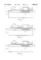
- FIG. 1 is a cross-sectional view of the structure 10 of the present invention including a metal layer 12 with an extension area 12a.
- a die 14 with its associated layers including an original wire bond pad 16 and passivation layer 18.
- the original wire bond pad 16 is typically made of aluminum, an aluminum/silicon alloy or an aluminum/silicon/copper alloy.
- the passivation layer 18 is made of a dielectric material and is typically formed of oxide and/or nitride layer(s). In one embodiment, the passivation layer 18 is made of silicon dioxide.
- the die 14 with the original die bond pad 16 and passivation layer 18 can be hermetically packaged.
- Metal layer 12 is electrically connected to the original die bond pad 16.
- the metal layer 12 extends beyond the original wire bond pad 16 to form the extension area 12a.
- the metal layer 12 is preferably positioned over the passivation layer 18.
- This metal layer 12 is preferably formed of a gold or solder material.
- the metal layer 12 is deposited as thin layer.
- a barrier layer 20 such as titanium/tungsten can be placed between the original die bond pad 16 and the additional metal layer 12. The barrier layer prevents an intermetallic interaction between the metal layer and the original wire bond pad 16. Otherwise a metal layer 12 of gold that directly contacts an original wire bond pad 16 of aluminum will generate an undesirable intermetallic interaction.
- the extension area 12a preferably extends over portions of the passivation layer 18, the area for electrically contacting the die is increased without changing the die design. If the original die bond pad were to be increased in size, an expensive re-design of the die would be required.
- the extension area 12a is preferably large enough to be connected with wire bonds. The minimum size of the extension area that would allow connection with a wire bond is currently a square about 50-100 microns on a side. Thus, the extension area preferably has an area 10,000 square microns or less, and an area preferably in the range of 2500-10,000 square microns. The extension area can be made smaller as the packaging connection area requirements are reduced in the future.
- a metal bump 24 can be produced in the area 22.
- This metal bump 24 is preferably made of gold.
- the metal bump 24 allows the die to be used in a flip chip or tape-automated-bonding (TAB) package. Additionally, the metal bump 24 can be created in a multi-bump process.
- the metal layer 12 is preferably made of material compatible with the material of the metal bump 24. In a preferred embodiment, both the metal layer 12 and the metal bump 24 are made of gold.
- a barrier layer 20 may optionally be provided prior to formation of metal layer 12.
- the barrier layer 20 can be deposited over the entire die surface.
- Patterned photoresist (not shown) is placed on top of the barrier layer 20, and the metal layer 12 is formed in a thin metal deposition.
- the metal layer 12 is a 3 micron thick deposition of gold.
- An additional layer of patterned photoresist is placed on the device, and the metal deposition for the metal bump 24 is done.
- the metal bump 24 is formed in a 25 micron thick deposition of gold.
- both the photoresist layers and the metal deposited on the photoresist layers are removed, leaving the metal layer 12 and the metal bump 24.
- a weak etch to the entire die surface can remove the barrier layer 20 at locations not covered by the metal layer 12.
- the extension areas can be detached when the test connections are removed from the die.
- the wire bond connection can be stronger than the connection of the extension area to the die so that the extension areas can be removed from the die by simply pulling on the wire bonds. Having a relatively weak connection between the extension area and the die enhances this effect.
- FIGS. 2-5 illustrate structures which aid in detaching the extension areas. Many of the techniques described in FIGS. 2-5 can be combined.
- FIG. 2 is a cross-sectional view of structures of the present invention showing a perforation at area 26.
- the perforations can be formed by using photoresist to produce openings juxtaposed in a line across the width of metallic layer 12. The perforation line is best seen with respect to FIG. 7 discussed below. The perforations facilitate removal of the extension area 12a.
- FIG. 3 is a cross-sectional view of the structure 30 of the present invention showing an extension area 12a without a barrier layer underneath. By omitting the barrier layer 20 underneath the extension area 12a, the removal of the extension area 12a may be made easier. Alternately, the edge of the barrier layer may terminate at point A.
- the structure of FIG. 3 requires a photoresist patterning step before the deposition of the barrier layer 20.
- FIG. 4 is a cross-sectional view of a structure 40 including an underlayer 42.
- a metal underlayer 42 is supplied below the metal layer 12.
- the metal underlayer comprises a metal material that forms a relatively weak alloy with the metal in the metal layer. This intermetallic interaction will weaken portions of the metal layer 12, thus making the extension area 12a easier to remove.
- an underlayer 42 made of aluminum causes an intermetallic interaction with the metal layer 12 made of gold. The gold migrates into the aluminum region, forming a relatively weak gold/aluminum intermetallic region (not shown). Voids or pits in this contact region may also be formed by the intermetallic process.
- the intermetallic interaction can be facilitated by heating the dies. In a preferred embodiment, the dies can be heated to 200° C.-300° C. for about an hour.
- the underlayer can be a metal that forms an intermetallic interaction with copper.
- FIG. 5 is a cross-sectional view of the structure 50 of the present invention showing an underlayer 52.
- Underlayer 52 forms a weak contact with the extension area 12a. The weak contact makes it easier for the extension area 12a to be removed.
- Underlayer 52 is preferably made of an epoxy or polyimide.
- FIGS. 6A-C are top views of the present invention illustrating the different locations for the extension area 60. Note that FIGS. 6B and 6C use a narrow portion 62 which aids in the removal of the extension areas 60. Also shown in these figures is the optional metal bump 64.
- FIG. 7 is a top view of structure of the present invention showing a perforation line 66 at the narrow region 62.
- the perforation line 66 includes openings 68 and metal regions 70.
- FIG. 8A is a cross-sectional view showing the structure of the present invention with a wire bond 92 connecting to the extension region 12a.
- the connection to the extension region 12a can be used to burn-in test the die.
- An intermetallic region 96 is formed where a metallic underlayer contacts a portion of the metal layer 12.
- FIG. 8B is a cross-sectional view showing the structure of the present invention with the extension region 12a being removed along with the wire bond 92.
- the extension area 12a peels away from the barrier layer 20 or the passivation layer 18. Because the intermetallic region 96 is weak and brittle, the extension area 12a detaches from the remainder of the metal layer 12 at the intermetallic region 96. If perforations (not shown) are formed in the metal layer, the extension area 12a will detach from the remainder of the metal layer 12 along the perforations (not shown). Perforations can be used by themselves or in conjunction with the intermetallic region. With the extension area 12a removed, the circuity below passivation layer 18 can be visually inspected.
- the final packaging connections can be made to the area 22 which has been untouched by the testing connection (i.e. wire bond 92).
- a detachment region can comprise the perforations and/or the intermetallic region. This detachment region prevents the metal layer from peeling back at area 22.
- FIG. 9 is a flow chart illustrating the method of the present invention.
- step 80 a die with die bond pads and a metal layer including extension areas is provided. This step is described above.
- electrical connections are made to the extension areas in step 82. This step can be done by connecting a probe to the extension areas in step 82a, connecting to extension areas with wire bonds to a test substrate in step 82b, or connecting to the extension areas and packaging the die for testing in step 82c.
- Step 84 comprises the burn-in testing of the die.
- step 86 the connections are removed from the extension areas.
- the extension areas can optionally be removed. At this point, the known-good-dies could be packaged making connections to locations other than the extension areas, in step 88.
- step 90 the unpackaged known-good-die could be provided to the customer.
- Another alternative is for the dies to be tested while they are on the wafer before the dies on the wafer are separated.
Abstract
Description
Claims (30)
Priority Applications (1)
| Application Number | Priority Date | Filing Date | Title |
|---|---|---|---|
| US08/717,411 US5886414A (en) | 1996-09-20 | 1996-09-20 | Removal of extended bond pads using intermetallics |
Applications Claiming Priority (1)
| Application Number | Priority Date | Filing Date | Title |
|---|---|---|---|
| US08/717,411 US5886414A (en) | 1996-09-20 | 1996-09-20 | Removal of extended bond pads using intermetallics |
Publications (1)
| Publication Number | Publication Date |
|---|---|
| US5886414A true US5886414A (en) | 1999-03-23 |
Family
ID=24881919
Family Applications (1)
| Application Number | Title | Priority Date | Filing Date |
|---|---|---|---|
| US08/717,411 Expired - Lifetime US5886414A (en) | 1996-09-20 | 1996-09-20 | Removal of extended bond pads using intermetallics |
Country Status (1)
| Country | Link |
|---|---|
| US (1) | US5886414A (en) |
Cited By (15)
| Publication number | Priority date | Publication date | Assignee | Title |
|---|---|---|---|---|
| US6008061A (en) * | 1996-10-11 | 1999-12-28 | Kabushiki Kaisha Toshiba | Method of manufacturing semiconductor device having a test pad |
| WO2000011718A1 (en) * | 1998-08-22 | 2000-03-02 | Mci Computer Gmbh | Flip-chip type electronic component |
| US20010031508A1 (en) * | 1999-05-28 | 2001-10-18 | Bae Systems - Information & Electronic Warfare Systems | Method and apparatus for evaluating a known good die using both wire bond and flip-chip interconnects |
| US6373143B1 (en) * | 1998-09-24 | 2002-04-16 | International Business Machines Corporation | Integrated circuit having wirebond pads suitable for probing |
| US20030146504A1 (en) * | 2002-02-05 | 2003-08-07 | Tae Yamane | Chip-size semiconductor package |
| US6693361B1 (en) * | 1999-12-06 | 2004-02-17 | Tru-Si Technologies, Inc. | Packaging of integrated circuits and vertical integration |
| US20040141028A1 (en) * | 2001-04-26 | 2004-07-22 | Hirotake Nakamura | Recording head unit, manufacturing method thereof, and recorder using the unit |
| US20040145061A1 (en) * | 2003-01-29 | 2004-07-29 | Tomonori Kanai | Semiconductor device |
| US20050017361A1 (en) * | 2003-07-23 | 2005-01-27 | Megic Corporation | Post-passivation metal scheme on an IC chip with copper interconnection |
| US7026721B2 (en) * | 1999-11-18 | 2006-04-11 | Taiwan Semiconductor Manufacturing Company, Ltd. | Method of improving copper pad adhesion |
| US20060076159A1 (en) * | 2004-10-12 | 2006-04-13 | International Business Machines Corporation | Contour structures to highlight inspection regions |
| US20070262456A1 (en) * | 1998-12-21 | 2007-11-15 | Mou-Shiung Lin | Top layers of metal for high performance IC's |
| US7956474B1 (en) * | 2005-03-23 | 2011-06-07 | Marvell International Ltd. | Structures, architectures, systems, methods, algorithms and software for configuring an integrated circuit for multiple packaging types |
| US8405220B1 (en) | 2005-03-23 | 2013-03-26 | Marvell International Ltd. | Structures, architectures, systems, methods, algorithms and software for configuring an integrated circuit for multiple packaging types |
| US20190221526A1 (en) * | 2014-04-14 | 2019-07-18 | Renesas Electronics Corporation | Semiconductor device and method of manufacturing the same |
Citations (20)
| Publication number | Priority date | Publication date | Assignee | Title |
|---|---|---|---|---|
| US3973271A (en) * | 1967-12-13 | 1976-08-03 | Matsushita Electronics Corporation | Semiconductor device having bonding pads extending over active regions |
| US4622574A (en) * | 1985-07-29 | 1986-11-11 | The Perkin-Elmer Corporation | Semiconductor chip with recessed bond pads |
| US4693770A (en) * | 1985-07-05 | 1987-09-15 | Matsushita Electric Industrial Co., Ltd. | Method of bonding semiconductor devices together |
| US4951098A (en) * | 1988-12-21 | 1990-08-21 | Eastman Kodak Company | Electrode structure for light emitting diode array chip |
| US4959706A (en) * | 1988-05-23 | 1990-09-25 | United Technologies Corporation | Integrated circuit having an improved bond pad |
| US4984065A (en) * | 1989-01-11 | 1991-01-08 | Kabushiki Kaisha Toshiba | Hybrid resin-sealed semiconductor device |
| US5053850A (en) * | 1988-03-14 | 1991-10-01 | Motorola, Inc. | Bonding pad for semiconductor devices |
| US5156997A (en) * | 1991-02-11 | 1992-10-20 | Microelectronics And Computer Technology Corporation | Method of making semiconductor bonding bumps using metal cluster ion deposition |
| US5367763A (en) * | 1993-09-30 | 1994-11-29 | Atmel Corporation | TAB testing of area array interconnected chips |
| US5384488A (en) * | 1992-06-15 | 1995-01-24 | Texas Instruments Incorporated | Configuration and method for positioning semiconductor device bond pads using additional process layers |
| US5394013A (en) * | 1990-11-28 | 1995-02-28 | Mitsubishi Denki Kabushiki Kaisha | Semiconductor device with an elevated bonding pad |
| US5404045A (en) * | 1991-10-19 | 1995-04-04 | Nec Corporation | Semiconductor device with an electrode pad having increased mechanical strength |
| US5483741A (en) * | 1993-09-03 | 1996-01-16 | Micron Technology, Inc. | Method for fabricating a self limiting silicon based interconnect for testing bare semiconductor dice |
| US5508229A (en) * | 1994-05-24 | 1996-04-16 | National Semiconductor Corporation | Method for forming solder bumps in semiconductor devices |
| US5508228A (en) * | 1994-02-14 | 1996-04-16 | Microelectronics And Computer Technology Corporation | Compliant electrically connective bumps for an adhesive flip chip integrated circuit device and methods for forming same |
| US5517127A (en) * | 1995-01-09 | 1996-05-14 | International Business Machines Corporation | Additive structure and method for testing semiconductor wire bond dies |
| US5541446A (en) * | 1994-08-29 | 1996-07-30 | Analog Devices, Inc. | Integrated circuit package with improved heat dissipation |
| US5631499A (en) * | 1994-04-28 | 1997-05-20 | Kabushiki Kaisha Toshiba | Semiconductor device comprising fine bump electrode having small side etch portion and stable characteristics |
| US5640762A (en) * | 1988-09-30 | 1997-06-24 | Micron Technology, Inc. | Method and apparatus for manufacturing known good semiconductor die |
| US5742100A (en) * | 1995-03-27 | 1998-04-21 | Motorola, Inc. | Structure having flip-chip connected substrates |
-
1996
- 1996-09-20 US US08/717,411 patent/US5886414A/en not_active Expired - Lifetime
Patent Citations (20)
| Publication number | Priority date | Publication date | Assignee | Title |
|---|---|---|---|---|
| US3973271A (en) * | 1967-12-13 | 1976-08-03 | Matsushita Electronics Corporation | Semiconductor device having bonding pads extending over active regions |
| US4693770A (en) * | 1985-07-05 | 1987-09-15 | Matsushita Electric Industrial Co., Ltd. | Method of bonding semiconductor devices together |
| US4622574A (en) * | 1985-07-29 | 1986-11-11 | The Perkin-Elmer Corporation | Semiconductor chip with recessed bond pads |
| US5053850A (en) * | 1988-03-14 | 1991-10-01 | Motorola, Inc. | Bonding pad for semiconductor devices |
| US4959706A (en) * | 1988-05-23 | 1990-09-25 | United Technologies Corporation | Integrated circuit having an improved bond pad |
| US5640762A (en) * | 1988-09-30 | 1997-06-24 | Micron Technology, Inc. | Method and apparatus for manufacturing known good semiconductor die |
| US4951098A (en) * | 1988-12-21 | 1990-08-21 | Eastman Kodak Company | Electrode structure for light emitting diode array chip |
| US4984065A (en) * | 1989-01-11 | 1991-01-08 | Kabushiki Kaisha Toshiba | Hybrid resin-sealed semiconductor device |
| US5394013A (en) * | 1990-11-28 | 1995-02-28 | Mitsubishi Denki Kabushiki Kaisha | Semiconductor device with an elevated bonding pad |
| US5156997A (en) * | 1991-02-11 | 1992-10-20 | Microelectronics And Computer Technology Corporation | Method of making semiconductor bonding bumps using metal cluster ion deposition |
| US5404045A (en) * | 1991-10-19 | 1995-04-04 | Nec Corporation | Semiconductor device with an electrode pad having increased mechanical strength |
| US5384488A (en) * | 1992-06-15 | 1995-01-24 | Texas Instruments Incorporated | Configuration and method for positioning semiconductor device bond pads using additional process layers |
| US5483741A (en) * | 1993-09-03 | 1996-01-16 | Micron Technology, Inc. | Method for fabricating a self limiting silicon based interconnect for testing bare semiconductor dice |
| US5367763A (en) * | 1993-09-30 | 1994-11-29 | Atmel Corporation | TAB testing of area array interconnected chips |
| US5508228A (en) * | 1994-02-14 | 1996-04-16 | Microelectronics And Computer Technology Corporation | Compliant electrically connective bumps for an adhesive flip chip integrated circuit device and methods for forming same |
| US5631499A (en) * | 1994-04-28 | 1997-05-20 | Kabushiki Kaisha Toshiba | Semiconductor device comprising fine bump electrode having small side etch portion and stable characteristics |
| US5508229A (en) * | 1994-05-24 | 1996-04-16 | National Semiconductor Corporation | Method for forming solder bumps in semiconductor devices |
| US5541446A (en) * | 1994-08-29 | 1996-07-30 | Analog Devices, Inc. | Integrated circuit package with improved heat dissipation |
| US5517127A (en) * | 1995-01-09 | 1996-05-14 | International Business Machines Corporation | Additive structure and method for testing semiconductor wire bond dies |
| US5742100A (en) * | 1995-03-27 | 1998-04-21 | Motorola, Inc. | Structure having flip-chip connected substrates |
Cited By (47)
| Publication number | Priority date | Publication date | Assignee | Title |
|---|---|---|---|---|
| US6008061A (en) * | 1996-10-11 | 1999-12-28 | Kabushiki Kaisha Toshiba | Method of manufacturing semiconductor device having a test pad |
| WO2000011718A1 (en) * | 1998-08-22 | 2000-03-02 | Mci Computer Gmbh | Flip-chip type electronic component |
| US6429675B2 (en) * | 1998-09-24 | 2002-08-06 | International Business Machines Corporation | Structure and method for probing wiring bond pads |
| US6373143B1 (en) * | 1998-09-24 | 2002-04-16 | International Business Machines Corporation | Integrated circuit having wirebond pads suitable for probing |
| US8022545B2 (en) | 1998-12-21 | 2011-09-20 | Megica Corporation | Top layers of metal for high performance IC's |
| US20070278686A1 (en) * | 1998-12-21 | 2007-12-06 | Mou-Shiung Lin | Top layers of metal for high performance IC's |
| US20090045516A1 (en) * | 1998-12-21 | 2009-02-19 | Megica Corporation | TOP LAYERS OF METAL FOR HIGH PERFORMANCE IC's |
| US8531038B2 (en) | 1998-12-21 | 2013-09-10 | Megica Corporation | Top layers of metal for high performance IC's |
| US8471384B2 (en) | 1998-12-21 | 2013-06-25 | Megica Corporation | Top layers of metal for high performance IC's |
| US8415800B2 (en) | 1998-12-21 | 2013-04-09 | Megica Corporation | Top layers of metal for high performance IC's |
| US20070290358A1 (en) * | 1998-12-21 | 2007-12-20 | Mou-Shiung Lin | Top layers of metal for high performance IC's |
| US20070288880A1 (en) * | 1998-12-21 | 2007-12-13 | Mou-Shiung Lin | Top layers of metal for high performance IC's |
| US20070281458A1 (en) * | 1998-12-21 | 2007-12-06 | Mou-Shiung Lin | Top layers of metal for high performance IC's |
| US20070273033A1 (en) * | 1998-12-21 | 2007-11-29 | Mou-Shiung Lin | Top layers of metal for high performance IC's |
| US7999384B2 (en) | 1998-12-21 | 2011-08-16 | Megica Corporation | Top layers of metal for high performance IC's |
| US7884479B2 (en) | 1998-12-21 | 2011-02-08 | Megica Corporation | Top layers of metal for high performance IC's |
| US20070262456A1 (en) * | 1998-12-21 | 2007-11-15 | Mou-Shiung Lin | Top layers of metal for high performance IC's |
| US20070262457A1 (en) * | 1998-12-21 | 2007-11-15 | Mou-Shiung Lin | Top layers of metal for high performance IC's |
| US20070267714A1 (en) * | 1998-12-21 | 2007-11-22 | Mou-Shiung Lin | Top layers of metal for high performance IC's |
| US7863654B2 (en) | 1998-12-21 | 2011-01-04 | Megica Corporation | Top layers of metal for high performance IC's |
| US20010031508A1 (en) * | 1999-05-28 | 2001-10-18 | Bae Systems - Information & Electronic Warfare Systems | Method and apparatus for evaluating a known good die using both wire bond and flip-chip interconnects |
| USRE43607E1 (en) * | 1999-05-28 | 2012-08-28 | Jones Farm Technology, Llc | Method and apparatus for evaluating a known good die using both wire bond and flip-chip interconnects |
| US6900654B2 (en) * | 1999-05-28 | 2005-05-31 | Bae Systems - Information & Electronic Warfare Systems | Method and apparatus for evaluating a known good die using both wire bond and flip-chip interconnects |
| US7026721B2 (en) * | 1999-11-18 | 2006-04-11 | Taiwan Semiconductor Manufacturing Company, Ltd. | Method of improving copper pad adhesion |
| US6693361B1 (en) * | 1999-12-06 | 2004-02-17 | Tru-Si Technologies, Inc. | Packaging of integrated circuits and vertical integration |
| US20040141028A1 (en) * | 2001-04-26 | 2004-07-22 | Hirotake Nakamura | Recording head unit, manufacturing method thereof, and recorder using the unit |
| US7258423B2 (en) * | 2001-04-26 | 2007-08-21 | Brother Kogyo Kabushiki Kaisha | Recording head unit, method of manufacturing the same, and recording apparatus using the unit |
| US20030146504A1 (en) * | 2002-02-05 | 2003-08-07 | Tae Yamane | Chip-size semiconductor package |
| US6987323B2 (en) * | 2002-02-05 | 2006-01-17 | Oki Electric Industry Co., Ltd. | Chip-size semiconductor package |
| US20040145061A1 (en) * | 2003-01-29 | 2004-07-29 | Tomonori Kanai | Semiconductor device |
| US7205671B2 (en) * | 2003-01-29 | 2007-04-17 | Hitachi Maxell, Ltd. | Semiconductor device |
| US7470997B2 (en) * | 2003-07-23 | 2008-12-30 | Megica Corporation | Wirebond pad for semiconductor chip or wafer |
| US20050017361A1 (en) * | 2003-07-23 | 2005-01-27 | Megic Corporation | Post-passivation metal scheme on an IC chip with copper interconnection |
| US7411135B2 (en) | 2004-10-12 | 2008-08-12 | International Business Machines Corporation | Contour structures to highlight inspection regions |
| US7614147B2 (en) | 2004-10-12 | 2009-11-10 | International Business Machines Corporation | Method of creating contour structures to highlight inspection region |
| US20060076159A1 (en) * | 2004-10-12 | 2006-04-13 | International Business Machines Corporation | Contour structures to highlight inspection regions |
| US20080244904A1 (en) * | 2004-10-12 | 2008-10-09 | International Business Machines Corporation | Contour Structures to Highlight Inspection Regions |
| US7956474B1 (en) * | 2005-03-23 | 2011-06-07 | Marvell International Ltd. | Structures, architectures, systems, methods, algorithms and software for configuring an integrated circuit for multiple packaging types |
| US8455347B1 (en) | 2005-03-23 | 2013-06-04 | Marvell International Ltd. | Structures, architectures, systems, methods, algorithms and software for configuring an integrated circuit for multiple packaging types |
| US8405220B1 (en) | 2005-03-23 | 2013-03-26 | Marvell International Ltd. | Structures, architectures, systems, methods, algorithms and software for configuring an integrated circuit for multiple packaging types |
| US8963342B1 (en) | 2005-03-23 | 2015-02-24 | Marvell International Ltd. | Structures, architectures, systems, methods, algorithms and software for configuring an integrated circuit for multiple packaging types |
| US9524927B1 (en) | 2005-03-23 | 2016-12-20 | Marvell International Ltd. | Structures, architectures, systems, methods, algorithms and software for configuring an integrated circuit for multiple packaging types |
| US20190221526A1 (en) * | 2014-04-14 | 2019-07-18 | Renesas Electronics Corporation | Semiconductor device and method of manufacturing the same |
| US10923437B2 (en) * | 2014-04-14 | 2021-02-16 | Renesas Electronics Corporation | Semiconductor device and method of manufacturing the same |
| US11482498B2 (en) | 2014-04-14 | 2022-10-25 | Renesas Electronics Corporation | Semiconductor device and method of manufacturing the same |
| US20230015101A1 (en) * | 2014-04-14 | 2023-01-19 | Renesas Electronics Corporation | Semiconductor device and method of manufacturing the same |
| US11810869B2 (en) * | 2014-04-14 | 2023-11-07 | Renesas Electronics Corporation | Semiconductor device and method of manufacturing the same |
Similar Documents
| Publication | Publication Date | Title |
|---|---|---|
| US5783868A (en) | Extended bond pads with a plurality of perforations | |
| US5886414A (en) | Removal of extended bond pads using intermetallics | |
| US5844317A (en) | Consolidated chip design for wire bond and flip-chip package technologies | |
| US6204074B1 (en) | Chip design process for wire bond and flip-chip package | |
| US5378981A (en) | Method for testing a semiconductor device on a universal test circuit substrate | |
| US5593903A (en) | Method of forming contact pads for wafer level testing and burn-in of semiconductor dice | |
| US5854513A (en) | Semiconductor device having a bump structure and test electrode | |
| US5517127A (en) | Additive structure and method for testing semiconductor wire bond dies | |
| US6730529B1 (en) | Method for chip testing | |
| JPH08504036A (en) | Area array wiring chip TAB test | |
| US20030155940A1 (en) | Method for forming cantilever beam probe card and probe card formed | |
| US6166556A (en) | Method for testing a semiconductor device and semiconductor device tested thereby | |
| US8232113B2 (en) | Method for manufacturing and testing an integrated electronic circuit | |
| JPH0829451A (en) | Bump semiconductor device and probe inspection method thereof | |
| US7538346B2 (en) | Semiconductor device | |
| JP2002090422A (en) | Semiconductor device and its manufacturing method | |
| US6861749B2 (en) | Semiconductor device with bump electrodes | |
| JPH06326111A (en) | Formation method for bump on semiconductor element | |
| TWI288464B (en) | Circuit under pad and method of forming a pad | |
| US6563226B2 (en) | Bonding pad | |
| JPH10116834A (en) | Method of manufacturing semiconductor device | |
| JP2001127256A (en) | Semiconductor device | |
| JPH08340029A (en) | Flip chip ic and its manufacture | |
| US6972583B2 (en) | Method for testing electrical characteristics of bumps | |
| JPH02184043A (en) | Manufacture of semiconductor device |
Legal Events
| Date | Code | Title | Description |
|---|---|---|---|
| AS | Assignment |
Owner name: DEVICE TECHNOLOGY, INC., A CORP. OF DE, CALIFORNIA Free format text: ASSIGNMENT OF ASSIGNORS INTEREST;ASSIGNOR:GALLOWAY, TERRY R.;REEL/FRAME:008254/0945 Effective date: 19960912 |
|
| STCF | Information on status: patent grant |
Free format text: PATENTED CASE |
|
| FEPP | Fee payment procedure |
Free format text: PAYOR NUMBER ASSIGNED (ORIGINAL EVENT CODE: ASPN); ENTITY STATUS OF PATENT OWNER: LARGE ENTITY |
|
| FPAY | Fee payment |
Year of fee payment: 4 |
|
| REMI | Maintenance fee reminder mailed | ||
| REMI | Maintenance fee reminder mailed | ||
| FPAY | Fee payment |
Year of fee payment: 8 |
|
| SULP | Surcharge for late payment |
Year of fee payment: 7 |
|
| FPAY | Fee payment |
Year of fee payment: 12 |