US6005707A - Optical devices comprising polymer-dispersed crystalline materials - Google Patents
Optical devices comprising polymer-dispersed crystalline materials Download PDFInfo
- Publication number
- US6005707A US6005707A US08/976,002 US97600297A US6005707A US 6005707 A US6005707 A US 6005707A US 97600297 A US97600297 A US 97600297A US 6005707 A US6005707 A US 6005707A
- Authority
- US
- United States
- Prior art keywords
- optical material
- crystalline
- optical
- fluorinated
- polymer
- Prior art date
- Legal status (The legal status is an assumption and is not a legal conclusion. Google has not performed a legal analysis and makes no representation as to the accuracy of the status listed.)
- Expired - Lifetime
Links
Images


Classifications
-
- G—PHYSICS
- G02—OPTICS
- G02F—OPTICAL DEVICES OR ARRANGEMENTS FOR THE CONTROL OF LIGHT BY MODIFICATION OF THE OPTICAL PROPERTIES OF THE MEDIA OF THE ELEMENTS INVOLVED THEREIN; NON-LINEAR OPTICS; FREQUENCY-CHANGING OF LIGHT; OPTICAL LOGIC ELEMENTS; OPTICAL ANALOGUE/DIGITAL CONVERTERS
- G02F1/00—Devices or arrangements for the control of the intensity, colour, phase, polarisation or direction of light arriving from an independent light source, e.g. switching, gating or modulating; Non-linear optics
- G02F1/01—Devices or arrangements for the control of the intensity, colour, phase, polarisation or direction of light arriving from an independent light source, e.g. switching, gating or modulating; Non-linear optics for the control of the intensity, phase, polarisation or colour
- G02F1/015—Devices or arrangements for the control of the intensity, colour, phase, polarisation or direction of light arriving from an independent light source, e.g. switching, gating or modulating; Non-linear optics for the control of the intensity, phase, polarisation or colour based on semiconductor elements with at least one potential jump barrier, e.g. PN, PIN junction
- G02F1/017—Structures with periodic or quasi periodic potential variation, e.g. superlattices, quantum wells
-
- B—PERFORMING OPERATIONS; TRANSPORTING
- B82—NANOTECHNOLOGY
- B82Y—SPECIFIC USES OR APPLICATIONS OF NANOSTRUCTURES; MEASUREMENT OR ANALYSIS OF NANOSTRUCTURES; MANUFACTURE OR TREATMENT OF NANOSTRUCTURES
- B82Y20/00—Nanooptics, e.g. quantum optics or photonic crystals
-
- G—PHYSICS
- G02—OPTICS
- G02F—OPTICAL DEVICES OR ARRANGEMENTS FOR THE CONTROL OF LIGHT BY MODIFICATION OF THE OPTICAL PROPERTIES OF THE MEDIA OF THE ELEMENTS INVOLVED THEREIN; NON-LINEAR OPTICS; FREQUENCY-CHANGING OF LIGHT; OPTICAL LOGIC ELEMENTS; OPTICAL ANALOGUE/DIGITAL CONVERTERS
- G02F1/00—Devices or arrangements for the control of the intensity, colour, phase, polarisation or direction of light arriving from an independent light source, e.g. switching, gating or modulating; Non-linear optics
- G02F1/01—Devices or arrangements for the control of the intensity, colour, phase, polarisation or direction of light arriving from an independent light source, e.g. switching, gating or modulating; Non-linear optics for the control of the intensity, phase, polarisation or colour
- G02F1/015—Devices or arrangements for the control of the intensity, colour, phase, polarisation or direction of light arriving from an independent light source, e.g. switching, gating or modulating; Non-linear optics for the control of the intensity, phase, polarisation or colour based on semiconductor elements with at least one potential jump barrier, e.g. PN, PIN junction
- G02F1/0151—Devices or arrangements for the control of the intensity, colour, phase, polarisation or direction of light arriving from an independent light source, e.g. switching, gating or modulating; Non-linear optics for the control of the intensity, phase, polarisation or colour based on semiconductor elements with at least one potential jump barrier, e.g. PN, PIN junction modulating the refractive index
- G02F1/0153—Devices or arrangements for the control of the intensity, colour, phase, polarisation or direction of light arriving from an independent light source, e.g. switching, gating or modulating; Non-linear optics for the control of the intensity, phase, polarisation or colour based on semiconductor elements with at least one potential jump barrier, e.g. PN, PIN junction modulating the refractive index using electro-refraction, e.g. Kramers-Kronig relation
-
- G—PHYSICS
- G02—OPTICS
- G02F—OPTICAL DEVICES OR ARRANGEMENTS FOR THE CONTROL OF LIGHT BY MODIFICATION OF THE OPTICAL PROPERTIES OF THE MEDIA OF THE ELEMENTS INVOLVED THEREIN; NON-LINEAR OPTICS; FREQUENCY-CHANGING OF LIGHT; OPTICAL LOGIC ELEMENTS; OPTICAL ANALOGUE/DIGITAL CONVERTERS
- G02F1/00—Devices or arrangements for the control of the intensity, colour, phase, polarisation or direction of light arriving from an independent light source, e.g. switching, gating or modulating; Non-linear optics
- G02F1/01—Devices or arrangements for the control of the intensity, colour, phase, polarisation or direction of light arriving from an independent light source, e.g. switching, gating or modulating; Non-linear optics for the control of the intensity, phase, polarisation or colour
- G02F1/015—Devices or arrangements for the control of the intensity, colour, phase, polarisation or direction of light arriving from an independent light source, e.g. switching, gating or modulating; Non-linear optics for the control of the intensity, phase, polarisation or colour based on semiconductor elements with at least one potential jump barrier, e.g. PN, PIN junction
- G02F1/0155—Devices or arrangements for the control of the intensity, colour, phase, polarisation or direction of light arriving from an independent light source, e.g. switching, gating or modulating; Non-linear optics for the control of the intensity, phase, polarisation or colour based on semiconductor elements with at least one potential jump barrier, e.g. PN, PIN junction modulating the optical absorption
- G02F1/0157—Devices or arrangements for the control of the intensity, colour, phase, polarisation or direction of light arriving from an independent light source, e.g. switching, gating or modulating; Non-linear optics for the control of the intensity, phase, polarisation or colour based on semiconductor elements with at least one potential jump barrier, e.g. PN, PIN junction modulating the optical absorption using electro-absorption effects, e.g. Franz-Keldysh [FK] effect or quantum confined stark effect [QCSE]
-
- G—PHYSICS
- G02—OPTICS
- G02F—OPTICAL DEVICES OR ARRANGEMENTS FOR THE CONTROL OF LIGHT BY MODIFICATION OF THE OPTICAL PROPERTIES OF THE MEDIA OF THE ELEMENTS INVOLVED THEREIN; NON-LINEAR OPTICS; FREQUENCY-CHANGING OF LIGHT; OPTICAL LOGIC ELEMENTS; OPTICAL ANALOGUE/DIGITAL CONVERTERS
- G02F1/00—Devices or arrangements for the control of the intensity, colour, phase, polarisation or direction of light arriving from an independent light source, e.g. switching, gating or modulating; Non-linear optics
- G02F1/01—Devices or arrangements for the control of the intensity, colour, phase, polarisation or direction of light arriving from an independent light source, e.g. switching, gating or modulating; Non-linear optics for the control of the intensity, phase, polarisation or colour
- G02F1/015—Devices or arrangements for the control of the intensity, colour, phase, polarisation or direction of light arriving from an independent light source, e.g. switching, gating or modulating; Non-linear optics for the control of the intensity, phase, polarisation or colour based on semiconductor elements with at least one potential jump barrier, e.g. PN, PIN junction
- G02F1/017—Structures with periodic or quasi periodic potential variation, e.g. superlattices, quantum wells
- G02F1/01708—Structures with periodic or quasi periodic potential variation, e.g. superlattices, quantum wells in an optical wavequide structure
-
- G—PHYSICS
- G02—OPTICS
- G02F—OPTICAL DEVICES OR ARRANGEMENTS FOR THE CONTROL OF LIGHT BY MODIFICATION OF THE OPTICAL PROPERTIES OF THE MEDIA OF THE ELEMENTS INVOLVED THEREIN; NON-LINEAR OPTICS; FREQUENCY-CHANGING OF LIGHT; OPTICAL LOGIC ELEMENTS; OPTICAL ANALOGUE/DIGITAL CONVERTERS
- G02F1/00—Devices or arrangements for the control of the intensity, colour, phase, polarisation or direction of light arriving from an independent light source, e.g. switching, gating or modulating; Non-linear optics
- G02F1/01—Devices or arrangements for the control of the intensity, colour, phase, polarisation or direction of light arriving from an independent light source, e.g. switching, gating or modulating; Non-linear optics for the control of the intensity, phase, polarisation or colour
- G02F1/015—Devices or arrangements for the control of the intensity, colour, phase, polarisation or direction of light arriving from an independent light source, e.g. switching, gating or modulating; Non-linear optics for the control of the intensity, phase, polarisation or colour based on semiconductor elements with at least one potential jump barrier, e.g. PN, PIN junction
- G02F1/017—Structures with periodic or quasi periodic potential variation, e.g. superlattices, quantum wells
- G02F1/01791—Quantum boxes or quantum dots
Definitions
- the invention relates to optical modulators and switches for use in telecommunications systems comprising solid-state crystalline optical material disposed between electrodes and, in particular, to such modulators wherein the crystalline material is comprised of III-V, II-VI or IV semiconductor nanocrystals embedded in a polymer matrix.
- the invention further relates to a method for making the optical crystalline material.
- Integrated circuits are being fabricated in smaller sizes and with electronic circuitry operable at increasingly higher speeds. As the operative speed of electronic circuits increases, it is becoming increasingly more difficult to transmit electrical signals between integrated circuits and boards. For this reason, there is growing interest in developing faster optical interconnect technologies that are operable at high frequencies and compatible with the silicon technology used in integrated circuits.
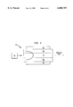
- an optical communication device 10 may comprise a crystal unit 12 sandwiched between first and second electrodes 14, 16, with a power source 15 coupled to the electrodes. Power is applied to the electrodes 14, 16, and a laser 20 is activated to emit a laser beam following the arrow L in FIG. 1A.
- the laser may be a semiconductor laser, a HeNe laser (632 nm) or the like.
- the crystal unit 12 is influenced by the applied electric field, and the intensity or phase of the light passing through the crystal unit is changed.
- the modulator may be coupled to a detector 18 for receiving the light and detecting the variation in the polarization of the light beam to define an optical communication system.
- KDP potassium dihydrogen phosphate
- ADP aluminum dihydrogen phosphate
- Single-crystal cadmium telluride and gallium arsenide optical materials are well known, but they typically have not been operable at extremely high frequencies. Also, integration with Si-based circuits could be problematic.
- Electro-optical modulators also have been described using crystal units comprising organic liquid crystals dispersed in a polymeric material, as shown in U.S. Pat. No. 5,132,814, to Ohkouchi et al, entitled “Liquid Crystal Spatial Light Modulator with Multi-layer Photoconductor,” and U.S. Pat. No. 5,011,624, to Yamagishi et al., entitled “Acryate PolymerDispersed Liquid Crystal Material and Device Made Therefrom.”
- encapsulated or polymeric-dispersed organic liquid crystal units have advantages, it is difficult to control liquid crystal composites during preparation. Often, liquid crystal droplets have irregular sizes and shapes such that the crystalline material may vary from region to region in its response to the applied electric field.
- organic liquid crystals are generally temperature-sensitive and thermally instable, and the crystalline material may form a clear liquid at increased temperatures.
- modulators typically do not operate at the high speeds desired for optical data transmission applications.
- Nanocrystal-polymer composites have been explored for applications other than optical modulators, that is, for use in light emitting diodes and photoconductors where for most purposes a fast response tme is not essential. See Alivisatos, "Semiconductor Clusters, Nanocrystals, and Quantum Dots," SCIENCE, Vol. 271 (Feb. 16, 1996), at pp. 933-36, which is hereby incorporated by reference.
- the present invention provides improved crystalline materials exhibiting high peak differential absorbance and refractive index changes that may be used in electro-optical modulators operable at high frequencies and at a broad range of wavelengths. Further features, characteristics, and advantages may appear more fully upon consideration of the detailed description given below.
- the crystalline material comprises CdSe crystals sized at less than 5.8 nm in diameter and more preferably at less than about 4 nm in diameter and advantageously embedded in poly(vinyl pyridine).
- the crystalline material sandwiched between two electrodes defines an optical modulator.
- the crystalline material with ten-percent crystal embedded in a polymer exhibits with an applied voltage of 0.5 to 100V, a differential absorbance spectra ( ⁇ A) of about 5 to 300 cm -1 at wavelengths of about 600 nm to 650 nm and a differential refractive index ( ⁇ n) of about 10 -5 to 10 -3 .
- the crystalline material may be made by dissolving the crystals in a monomer followed with polymerization to provide a resultant polymer-nanocrystal matrix.
- FIG. 1A is a cross-sectional view of a optical modulator in which the inventive crystalline material may be used;
- FIG. 1B is a schematic view of an optical communication system having an optical modulator in which the inventive crystalline material may be used;
- FIG. 2 is a graph illustrating the differential absorbance spectra of the inventive crystalline material involving a 10 percent crystal composite when a voltage of 100V is applied;
- FIG. 3 is a graph showing the change in refractive index of the inventive crystalline material calculated from the data of FIG. 2.
- FIG. 4 is a cross-sectional view of a planar waveguide device in which the inventive optical crystalline material may be used.
- III-V, II-VI or IV semiconductor nanocrystals may be synthesized that are substantially monodisperse and embedded in a polymer material to provide active materials for use in optical devices that exhibit distinct excitonic absorption features at room temperature.
- the crystalline material comprises about 4nm in diameter-sized CdSe nanocrystals embedded in a polymer.
- Advantageous polymers comprise poly(vinyl pyridine) and polystyrene.
- Other crystalline materials may comprise CdTe, InP, Si, InGaAs, and CdS.
- the electroabsorption spectra of the nanocrystal composites have been measured over a range of electric fields.
- the changes in absorption spectra and refractive index with the applied field are qualitatively significant, and further, the anticipated differential absorption spectra as a function of crystal size may be calculated with the assumption that the nanocrystals comprise quantum dots or zero dimensional materials.
- Modulators and switches comprising these crystals can be used in conjunction with semiconductor lasers and Si-based photodetectors to create optical interconnection systems, as illustrated in FIGS. 1A, 1B, and 4.
- the discussion below is dividing into three parts. Part A addresses various features and characteristics of various embodiments of the inventive crystalline material; Part B describes an exemplary method of synthesis; and Part C discusses exemplary applications for the crystalline material.
- FIGS. 2 and 3 show the differential absorbance spectra and differential refractive index, respectively, at room temperature for one embodiment of the inventive crystalline material.
- the data of FIG. 2 was experimentally obtained and the refractive index data of FIG. 3 was calculated from the absorbance data considering Kramers-Kronig relations, as is well known.
- the data of FIG. 2 reflects a crystalline material synthesized according to the Example of Part B, below, comprised of 4 nm in diameter sized CdSe nanocrystals dispersed in poly-4-vinylpyridine with a 10% by volume CdSe nanocrystal content in the polymer film, although the data was recorded with a 100% CdSe crystal which was then weighted to 10%.
- the crystalline material was sandwiched between two pieces of indium tin oxide (ITO) coated glass.
- ITO-glass was substantially transparent with the conducting ITO functioning as electrodes, and a voltage of 100V was applied between the two ITO-glass electrodes. With this applied voltage the absorbance data was recorded for a broad range of wavelengths, as can be seen in FIG. 2, with the material exhibiting a differential absorbance ( ⁇ A) of about 50 cm -1 at wavelengths of about 625 nm.
- the absorbance (A) was lowest at 50 cm -1 at wavelengths at and above about 625 nm.
- a differential refractive index ( ⁇ n) of about 10 -1 was calculated for wavelengths of about 625 nm.
- ⁇ A peak differential absorbance
- ⁇ A differential absorbance
- ⁇ A differential absorbance
- ⁇ n differential refractive index
- the value for ⁇ A and ⁇ n will be affected by the synthesis techniques, and the particular crystalline materials and particle sizes used. As the synthesis procedures are modified to increase the monodispersity of the particles, the values for ⁇ A and ⁇ n will likewise increase to provide a more effective electro-optical material.
- FIGS. 2 and 3 Although the data for FIGS. 2 and 3 was obtained using a CdSe crystal and a poly-4-vinylpyridine host polymer, other materials may be used. Polyimides, acrylates, or polymers of photopolymerizable monomers may be used, for example. Other polymers that also may be used comprise polystyrene and fluorinated polymers including fluoroacrylates, fluoromethacrylates, fluorinated acrylamides, fluorinated urethanes, fluorinated epoxies, fluorinated vinyl esters, and co-polymers and mixtures of such polymers. Other III-V and II-VI semiconductor nanocrystals may comprise CdTe, CdSe, InP, and InGaAs. In addition, the use of Si (Group IV) nanocrystals is contemplated.
- Si Group IV
- the crystal size could be varied to obtain modulation at desired wavelengths.
- GaAs-based laser technologies are well known, involving light beams of 630 to 830 nm.
- Crystalline materials may be fabricated for use in modulators operable at such wavelengths and combined with GaAs lasers.
- One may calculate the desired crystal size and anticipated absorption spectra characteristics for these wavelengths with the assumption that the particles comprise zero dimensional materials. Changes in absorption spectra may be determined when we consider the particles to comprise zero dimensional materials.
- Many optical properties of such nanocrystals change, sometimes drastically, with respect to bulk solids of the same material.
- the energy gap, E is increased due to quantum confinement effects to:
- Eg is the bandgap of the bulk solid
- R is the cluster radius
- ⁇ is the reduced mass
- e is the electronic charge
- ⁇ is the dielectric constant
- R y * is the effective Rydberg constant, which is known in the field and described in C. Kittel, INTRODUCTION TO SOLID STATE PHYSICS (5th Ed., John Wiley & Sons).
- the bandgap is an indicator of, and may be used to determine, the absorption spectra, as is well known.
- the density of states also changes from the parabolic density of states characteristic of bulk materials to, ideally, a set of discrete lines as in an atom. In real nanocrystals, however, the density of states is broadened due to differences in particle sizes, defects, and other imperfections.
- Equation 1 which is the energy difference between the lowest lying electron and hole bound states, can be lowered by the application of an electric field.
- This effect is called the Stark effect in atoms and in zero-dimensional solids such as nanocrystals. In quantum well systems, it is referred to as the "Quantum-confined Stark Effect".
- the changes in absorption specta with field of the inventive crystalline material are consisted with what one would expect as a result of the Quantum-confined Stark Effect of zero-dimensional materials.
- a crystalline material comprising CdSe crystals embedded in poly-4-vinylpyridine was fabricated with trioctylphosphine, trioctylphosphine oxide, dimethyl cadmium, elemental selenium, methanol, 1-butanol, and 4-vinylpyridine. These materials are commercially available. The 4-vinylpyridine was distilled immediately before use but the remaining materials were used without further purification.
- Trioctylphosphine selenide was first prepared by directly combining trioctylphosphine and elemental selenium. Two reagent solutions were then prepared, the first being 0.5 ml dimethyl cadmium in 12.5 ml trioctylphosphine, and the second being 5 ml. of a solution comprising a 1:1 mole ratio of trioctylphosphine selenide to trioctylphosphine plus an additional 7.5 ml trioctylphosphine. These two solutions were combined in the barrel of a 50 ml syringe fitted with a hypodermic needle.
- trioctylphosphine oxide 15 g trioctylphosphine oxide was degassed by heating under vacuum for about 15 minutes. After degassing, the temperature of the trioctylphosphine oxide was controlled to 300° C. While the trioctylphosphine oxide was vigorously stirred, the dimethyl cadmium and trioctylphosphine selenide solution was rapidly injected from the hypodermic needle. The mixture was maintained at about 200 to 250° C. for about 20 minutes and then allowed to cool to room temperature.
- the nanocrystal material was then separated by precipitating the crystalline solids with addition of methanol and dissolving the solids with 1-butanol to remove residues. More specifically, the mixture obtained with the above process was first heated from room temperature to about 60° C., just above the melting point of the solvent, and methanol was quickly added. The methanol precipitated a crystalline residue which was collected and redissolved in 1-butanol. The butanol solution was then filtered, and the filtered solution was added to several volumes of methanol to reprecipitate the solid crystalline residue. The solids were redissolved in butanol and reprecipitated with methanol several times. This process yielded nanocrystals of CdSe and a slight residue of trioctylphosphine and trioctylphosphine oxide.
- the nanocrystals were dispersed in poly-4-vinylpyridine as follows. Several milligrams of the nanocrystals were dissolved in 4vinylpyridine (distilled) and a small quantity of azobis(isobutyro)nitrile was added as a radical initiator, although other initiators could have been used, as is well known. The solution was heated to 70° C. for about 1 hour to initiate and carry out the polymerization. The resultant polymer-nanocrystal matrix that resulted was optically clear.
- the inventive crystalline optical material may be used to fabricate an optical display device, with the crystalline material comprising the crystal unit 2 disposed between the pair of electrodes 14, 16, and coupled to the power source 15.
- the electrodes 14, 16, may comprise indium-tin oxide (ITO), coated glass, as previously described.
- the crystal size may be adjusted to demonstrate a peak differential absorbance for the wavelength of the particular laser light beam contemplated.
- the waveguide modulator may be coupled to a detector to comprise an optical communication system, as schematically illustrated in FIG. 1B.
- the inventive crystalline material is used to fabricate a planar waveguide 30.
- the planar waveguide 30 comprises a core 32 disposed between two lower refractive index cladding layers 34a, 34b.
- the inventive crystalline material preferably constitutes the core, but it may be used for the cladding layers with a higher index material used for the core.
- the core comprises a 1 ⁇ m in thickness layer of CdSe dispersed in polystyrene, and each of the cladding layers 34a, 34b, comprises a 1 ⁇ m in thickness layer of poly(vinyl alcohol).
- a pair of electrodes 36, 38 for applying an electric field are placed adjacent the two cladding layers.
- the electrodes 36, 38 may comprise any metal.
- the applied electric field is dropped across both the core and cladding layers.
- the laser 20 is coupled to one end of the waveguide modulator adjacent the crystalline material, and the light is pumped directly into the crystalline material core or cladding to exit at the other end of the waveguide as a modulated light beam.
- the electric field is applied traverse to the path of the laser light beam.
- a longer device may be used to accomplish the light modulation (as compared with the optical display device of FIG. 1A), corresponding to a longer path for the light to travel through the crystalline material and a greater degree of modulation.
Abstract
Description
E=E.sub.g +h.sup.2 /2μ[π/R].sup.2 -1.786 e.sup.2 /εR-0.248 R.sub.y * (1),
Claims (14)
Priority Applications (3)
| Application Number | Priority Date | Filing Date | Title |
|---|---|---|---|
| US08/976,002 US6005707A (en) | 1997-11-21 | 1997-11-21 | Optical devices comprising polymer-dispersed crystalline materials |
| EP98309183A EP0918245A1 (en) | 1997-11-21 | 1998-11-10 | Optical devices comprising polymer-dispersed crystalline materials |
| JP10330490A JPH11223701A (en) | 1997-11-21 | 1998-11-20 | Optical material |
Applications Claiming Priority (1)
| Application Number | Priority Date | Filing Date | Title |
|---|---|---|---|
| US08/976,002 US6005707A (en) | 1997-11-21 | 1997-11-21 | Optical devices comprising polymer-dispersed crystalline materials |
Publications (1)
| Publication Number | Publication Date |
|---|---|
| US6005707A true US6005707A (en) | 1999-12-21 |
Family
ID=25523613
Family Applications (1)
| Application Number | Title | Priority Date | Filing Date |
|---|---|---|---|
| US08/976,002 Expired - Lifetime US6005707A (en) | 1997-11-21 | 1997-11-21 | Optical devices comprising polymer-dispersed crystalline materials |
Country Status (3)
| Country | Link |
|---|---|
| US (1) | US6005707A (en) |
| EP (1) | EP0918245A1 (en) |
| JP (1) | JPH11223701A (en) |
Cited By (56)
| Publication number | Priority date | Publication date | Assignee | Title |
|---|---|---|---|---|
| US6124964A (en) * | 1997-05-30 | 2000-09-26 | Hitachi, Ltd. | Organic/inorganic composite superlattice type optical modulator |
| WO2002065077A1 (en) * | 2001-02-09 | 2002-08-22 | Massachusetts Institute Of Technology | Temperature-sensing composition |
| US6496114B1 (en) * | 1998-01-22 | 2002-12-17 | Dkl International, Inc. | Method and apparatus using laser enhanced dielectrokinesis to locate entities |
| US6544732B1 (en) * | 1999-05-20 | 2003-04-08 | Illumina, Inc. | Encoding and decoding of array sensors utilizing nanocrystals |
| US20030085642A1 (en) * | 2001-07-20 | 2003-05-08 | Pelka David G. | Fluorescent light source |
| US20030127659A1 (en) * | 1998-04-01 | 2003-07-10 | Bawendi Moungi G. | Quantum dot white and colored light emitting diodes |
| US6599631B2 (en) | 2001-01-26 | 2003-07-29 | Nanogram Corporation | Polymer-inorganic particle composites |
| US6603243B2 (en) | 2000-03-06 | 2003-08-05 | Teledyne Technologies Incorporated | LED light source with field-of-view-controlling optics |
| US6637924B2 (en) | 2000-11-15 | 2003-10-28 | Teledyne Lighting And Display Products, Inc. | Strip lighting apparatus and method |
| US6710366B1 (en) | 2001-08-02 | 2004-03-23 | Ultradots, Inc. | Nanocomposite materials with engineered properties |
| US20040067431A1 (en) * | 2002-10-02 | 2004-04-08 | 3M Innovative Properties Company | Multiphoton photosensitization system |
| US20040067433A1 (en) * | 2002-10-02 | 2004-04-08 | 3M Innovative Properties Company | Multiphoton photosensitization method |
| US20040067451A1 (en) * | 2000-06-15 | 2004-04-08 | Devoe Robert J. | Multiphoton photochemical process and articles preparable thereby |
| US6744960B2 (en) * | 2000-03-06 | 2004-06-01 | Teledyne Lighting And Display Products, Inc. | Lighting apparatus having quantum dot layer |
| US20040152011A1 (en) * | 2002-12-09 | 2004-08-05 | Pixelligent Technologies Llc | Reversible photobleachable materials based on nano-sized semiconductor particles and their optical applications |
| US20040150023A1 (en) * | 2001-06-29 | 2004-08-05 | Jian Li | Low-voltage and interface damage-free polymer memory device |
| US6774560B1 (en) | 2000-09-19 | 2004-08-10 | The Regents Of The University Of California | Material system for tailorable white light emission and method for making thereof |
| US6794265B2 (en) | 2001-08-02 | 2004-09-21 | Ultradots, Inc. | Methods of forming quantum dots of Group IV semiconductor materials |
| US6819845B2 (en) | 2001-08-02 | 2004-11-16 | Ultradots, Inc. | Optical devices with engineered nonlinear nanocomposite materials |
| US7005669B1 (en) | 2001-08-02 | 2006-02-28 | Ultradots, Inc. | Quantum dots, nanocomposite materials with quantum dots, devices with quantum dots, and related fabrication methods |
| US7018853B1 (en) | 2001-07-20 | 2006-03-28 | Intel Corporation | Stepped structure for a multi-rank, stacked polymer memory device and method of making same |
| US20060154399A1 (en) * | 2000-04-24 | 2006-07-13 | Sauer Jon R | Ultra-fast nucleic acid sequencing device and a method for making and using the same |
| US20060163556A1 (en) * | 2005-01-21 | 2006-07-27 | Reiko Yoshimura | Refractive index variable device |
| WO2006113725A2 (en) * | 2005-04-18 | 2006-10-26 | The Regents Of The University Of California | Optical transceiver integratable with silicon vlsi |
| US20060279833A1 (en) * | 2005-05-30 | 2006-12-14 | Reiko Yoshimura | Refractive index variable element |
| US7226966B2 (en) | 2001-08-03 | 2007-06-05 | Nanogram Corporation | Structures incorporating polymer-inorganic particle blends |
| WO2007106770A2 (en) * | 2006-03-13 | 2007-09-20 | Evident Technologies | Semiconductor nanocryst al high-refractive index materials |
| US7358525B2 (en) | 2001-08-02 | 2008-04-15 | Ultradots, Inc. | Quantum dots of group IV semiconductor materials |
| US20080150184A1 (en) * | 2006-12-22 | 2008-06-26 | Shivkumar Chiruvolu | Composites of polymers and metal/metalloid oxide nanoparticles and methods for forming these composites |
| US20080176166A1 (en) * | 2006-07-10 | 2008-07-24 | Cooper Gregory D | Resists for lithography |
| US20080199687A1 (en) * | 2007-02-17 | 2008-08-21 | Shivkumar Chiruvolu | Functional composites, functional inks and applications thereof |
| US20080230120A1 (en) * | 2006-02-13 | 2008-09-25 | Solexant Corp. | Photovoltaic device with nanostructured layers |
| US20090001385A1 (en) * | 2007-06-27 | 2009-01-01 | Motorola, Inc. | Apparatus and method for modulating photon output of a quantum dot light emitting device |
| US20090035528A1 (en) * | 2002-10-02 | 2009-02-05 | 3M Innovative Properties Company | Multi-photon reacted articles with inorganic particles and method for fabricating structures |
| US20090081594A1 (en) * | 2003-03-04 | 2009-03-26 | Pixelligent Technologies Llc | Applications of semiconductor nano-sized particles for photolithography |
| US20090174022A1 (en) * | 2006-03-24 | 2009-07-09 | Seth Coe-Sullivan | Hyperspectral imaging device |
| US7566476B2 (en) | 1997-11-13 | 2009-07-28 | Massachusetts Institute Of Technology | Highly luminescent color-selective nanocrystalline materials |
| US20090191567A1 (en) | 1997-11-25 | 2009-07-30 | The Regents Of The University Of California | Semiconductor nanocrystal probes for biological applications and process for making and using such probes |
| US20100174024A1 (en) * | 2009-01-08 | 2010-07-08 | Hui Du | Composites of polysiloxane polymers and inorganic nanoparticles |
| US20100283036A1 (en) * | 2007-07-23 | 2010-11-11 | Seth Coe-Sullivan | Quantum dot light enhancement substrate and lighting device including same |
| US20100320442A1 (en) * | 2006-02-17 | 2010-12-23 | Solexant Corp. | Nanostructured electroluminescent device and display |
| US7887752B2 (en) | 2003-01-21 | 2011-02-15 | Illumina, Inc. | Chemical reaction monitor |
| CN102147537A (en) * | 2010-02-05 | 2011-08-10 | 财团法人中央大学校产学协力团 | Optical device using negative goos-hanchen shift |
| US8718437B2 (en) | 2006-03-07 | 2014-05-06 | Qd Vision, Inc. | Compositions, optical component, system including an optical component, devices, and other products |
| US8876272B2 (en) | 2007-06-25 | 2014-11-04 | Qd Vision, Inc. | Compositions and methods including depositing nanomaterial |
| US8993221B2 (en) | 2012-02-10 | 2015-03-31 | Pixelligent Technologies, Llc | Block co-polymer photoresist |
| US9006720B2 (en) | 2010-06-29 | 2015-04-14 | Nanogram Corporation | Silicon/germanium nanoparticles and inks having low metal contamination |
| US9023248B2 (en) | 2008-05-28 | 2015-05-05 | University Of Washington | Diels-Alder crosslinkable dendritic nonlinear optic chromophores and polymer composites |
| US9140844B2 (en) | 2008-05-06 | 2015-09-22 | Qd Vision, Inc. | Optical components, systems including an optical component, and devices |
| US9175174B2 (en) | 2000-10-17 | 2015-11-03 | Nanogram Corporation | Dispersions of submicron doped silicon particles |
| US9207385B2 (en) | 2008-05-06 | 2015-12-08 | Qd Vision, Inc. | Lighting systems and devices including same |
| US9349975B2 (en) | 2006-09-12 | 2016-05-24 | Qd Vision, Inc. | Composite including nanoparticles, methods, and products including a composite |
| US9475695B2 (en) | 2013-05-24 | 2016-10-25 | Nanogram Corporation | Printable inks with silicon/germanium based nanoparticles with high viscosity alcohol solvents |
| US9887316B2 (en) | 2011-04-01 | 2018-02-06 | Samsung Electronics Co., Ltd. | Quantum dots, method, and devices |
| US10145539B2 (en) | 2008-05-06 | 2018-12-04 | Samsung Electronics Co., Ltd. | Solid state lighting devices including quantum confined semiconductor nanoparticles, an optical component for a solid state lighting device, and methods |
| US10393940B2 (en) | 2006-03-07 | 2019-08-27 | Samsung Electronics Co., Ltd. | Compositions, optical component, system including an optical component, devices, and other products |
Families Citing this family (7)
| Publication number | Priority date | Publication date | Assignee | Title |
|---|---|---|---|---|
| AU2003229868A1 (en) * | 2002-03-19 | 2003-10-08 | Bookham Technology Plc | Tunable laser |
| GB2386965B (en) * | 2002-03-27 | 2005-09-07 | Bookham Technology Plc | Electro-optic modulators |
| AU2003234002A1 (en) * | 2002-05-15 | 2003-12-02 | Bookham Technology Plc | Tuneable laser |
| DE60325268D1 (en) | 2002-11-26 | 2009-01-22 | Elop Electrooptics Ind Ltd | PASSIVE-POWERED LASER |
| JP4383996B2 (en) | 2004-09-29 | 2009-12-16 | 株式会社東芝 | Refractive index changing device and refractive index changing method |
| JP2007065543A (en) * | 2005-09-02 | 2007-03-15 | Dainippon Printing Co Ltd | Variable optical element and optical device using the same |
| JP6878915B2 (en) * | 2017-01-26 | 2021-06-02 | 東洋インキScホールディングス株式会社 | Quantum dots and quantum dot-containing compositions |
Citations (1)
| Publication number | Priority date | Publication date | Assignee | Title |
|---|---|---|---|---|
| JPH10186426A (en) * | 1996-10-24 | 1998-07-14 | Mitsui Chem Inc | Photopolymerizable resin composition |
-
1997
- 1997-11-21 US US08/976,002 patent/US6005707A/en not_active Expired - Lifetime
-
1998
- 1998-11-10 EP EP98309183A patent/EP0918245A1/en not_active Withdrawn
- 1998-11-20 JP JP10330490A patent/JPH11223701A/en active Pending
Patent Citations (1)
| Publication number | Priority date | Publication date | Assignee | Title |
|---|---|---|---|---|
| JPH10186426A (en) * | 1996-10-24 | 1998-07-14 | Mitsui Chem Inc | Photopolymerizable resin composition |
Non-Patent Citations (8)
| Title |
|---|
| Akinow et al, Optika in Spekt. vol. 72, #4, pp. 1026-1032, abst. only herewith, Apr. 1992. |
| Akinow et al, Optika in Spekt. vol. 72, 4, pp. 1026 1032, abst. only herewith, Apr. 1992. * |
| Bawendi et al, Physical Review Letters, vol. 65, #13, pp. 162-1626; abst. only herewith, Sep. 24, 1990. |
| Bawendi et al, Physical Review Letters, vol. 65, 13, pp. 162 1626; abst. only herewith, Sep. 24, 1990. * |
| Salata O V et al. "Uniform GaAs Quatnum dots in a Polymer Matrix", Applied Physics Letters, Jul. 11, 1994, USA, vol. 65, No. 2, pp. 189-191. |
| Salata O V et al. Uniform GaAs Quatnum dots in a Polymer Matrix , Applied Physics Letters, Jul. 11, 1994, USA, vol. 65, No. 2, pp. 189 191. * |
| Woggon U et al. "Electro-Optic Properties of CdS Embedded in a Polymer", Physical Review B (Condensed Matter), Oct. 15, 1993, USA, vol. 48, No. 16, pp. 11979-11986. |
| Woggon U et al. Electro Optic Properties of CdS Embedded in a Polymer , Physical Review B (Condensed Matter), Oct. 15, 1993, USA, vol. 48, No. 16, pp. 11979 11986. * |
Cited By (140)
| Publication number | Priority date | Publication date | Assignee | Title |
|---|---|---|---|---|
| US6124964A (en) * | 1997-05-30 | 2000-09-26 | Hitachi, Ltd. | Organic/inorganic composite superlattice type optical modulator |
| US7566476B2 (en) | 1997-11-13 | 2009-07-28 | Massachusetts Institute Of Technology | Highly luminescent color-selective nanocrystalline materials |
| US8481113B2 (en) | 1997-11-13 | 2013-07-09 | Massachusetts Institute Of Technology | Highly luminescent color-selective nanocrystalline materials |
| US8481112B2 (en) | 1997-11-13 | 2013-07-09 | Massachusetts Institute Of Technology | Highly luminescent color-selective nanocrystalline materials |
| US8158193B2 (en) | 1997-11-13 | 2012-04-17 | Massachusetts Institute Of Technology | Highly luminescent color-selective nanocrystalline materials |
| US8101234B2 (en) | 1997-11-13 | 2012-01-24 | Massachusetts Institute Of Technology | Highly luminescent color-selective nanocrystalline materials |
| US9441156B2 (en) | 1997-11-13 | 2016-09-13 | Massachusetts Institute Of Technology | Highly luminescent color-selective nanocrystalline materials |
| US9790424B2 (en) | 1997-11-13 | 2017-10-17 | Massachusetts Institute Of Technology | Highly luminescent color-selective nanocrystalline materials |
| US8071359B2 (en) | 1997-11-25 | 2011-12-06 | The Regents Of The University Of California | Semiconductor nanocrystal probes for biological applications and process for making and using such probes |
| US8288152B2 (en) | 1997-11-25 | 2012-10-16 | The Regents Of The University Of California | Semiconductor nanocrystal probes for biological applications and process for making and using such probes |
| US8639449B2 (en) | 1997-11-25 | 2014-01-28 | The Regents Of The University Of California | Semiconductor nanocrystal probes for biological applications and process for making and using such probes |
| US8071361B2 (en) | 1997-11-25 | 2011-12-06 | The Regents Of The University Of California | Semiconductor nanocrystal probes for biological applications and process for making and using such probes |
| US20090191567A1 (en) | 1997-11-25 | 2009-07-30 | The Regents Of The University Of California | Semiconductor nanocrystal probes for biological applications and process for making and using such probes |
| US8071360B2 (en) | 1997-11-25 | 2011-12-06 | The Regents Of The University Of California | Semiconductor nanocrystal probes for biological applications and process for making and using such probes |
| US8288153B2 (en) | 1997-11-25 | 2012-10-16 | The Regents Of The University Of California | Semiconductor nanocrystal probes for biological applications and process for making and using such probes |
| US9530928B2 (en) | 1997-11-25 | 2016-12-27 | The Regents Of The University Of California | Semiconductor nanocrystal probes for biological applications and process for making and using such probes |
| US6496114B1 (en) * | 1998-01-22 | 2002-12-17 | Dkl International, Inc. | Method and apparatus using laser enhanced dielectrokinesis to locate entities |
| US8174181B2 (en) | 1998-04-01 | 2012-05-08 | Massachusetts Institute Of Technology | Quantum dot white and colored light-emitting devices |
| US7692373B2 (en) | 1998-04-01 | 2010-04-06 | Massachusetts Institute Of Technology | Quantum dot white and colored light-emitting devices |
| US20030127659A1 (en) * | 1998-04-01 | 2003-07-10 | Bawendi Moungi G. | Quantum dot white and colored light emitting diodes |
| US20100140585A1 (en) * | 1998-04-01 | 2010-06-10 | Massachusetts Institute Of Technology | Quantum dot white and colored light-emitting devices |
| US20080174233A1 (en) * | 1998-04-01 | 2008-07-24 | Massachusetts Institute Of Technology | Quantum dot white and colored light-emitting devices |
| US6890777B2 (en) * | 1998-04-01 | 2005-05-10 | Massachusetts Institute Of Technology | Quantum dot white and colored light emitting diodes |
| US20100176715A1 (en) * | 1998-04-01 | 2010-07-15 | Massachusetts Institute Of Technology | Quantum dot white and colored light-emitting devices |
| US8053972B2 (en) | 1998-04-01 | 2011-11-08 | Massachusetts Institute Of Technology | Quantum dot white and colored light-emitting devices |
| US20100141118A1 (en) * | 1998-04-01 | 2010-06-10 | Massachusetts Institute Of Technology | Quantum dot white and colored light-emitting devices |
| US20030175773A1 (en) * | 1999-05-20 | 2003-09-18 | Illumina, Inc. | Encoding and decoding of array sensors utilizing nanocrystals |
| US6544732B1 (en) * | 1999-05-20 | 2003-04-08 | Illumina, Inc. | Encoding and decoding of array sensors utilizing nanocrystals |
| US6890764B2 (en) | 1999-05-20 | 2005-05-10 | Illumina, Inc. | Encoding and decoding of array sensors utilizing nanocrystals |
| US6744960B2 (en) * | 2000-03-06 | 2004-06-01 | Teledyne Lighting And Display Products, Inc. | Lighting apparatus having quantum dot layer |
| US6603243B2 (en) | 2000-03-06 | 2003-08-05 | Teledyne Technologies Incorporated | LED light source with field-of-view-controlling optics |
| US9758824B2 (en) | 2000-04-24 | 2017-09-12 | Life Technologies Corporation | Ultra-fast nucleic acid sequencing device and a method for making and using the same |
| US20060154399A1 (en) * | 2000-04-24 | 2006-07-13 | Sauer Jon R | Ultra-fast nucleic acid sequencing device and a method for making and using the same |
| US9410923B2 (en) | 2000-04-24 | 2016-08-09 | Life Technologies Corporation | Ultra-fast nucleic acid sequencing device and a method for making and using the same |
| US9228976B2 (en) | 2000-04-24 | 2016-01-05 | Life Technologies Corporation | Method and apparatus for detecting nucleotides |
| US9063081B2 (en) | 2000-04-24 | 2015-06-23 | Life Technologies Corporation | Ultra-fast nucleic acid sequencing device and a method for making and using the same |
| US8232582B2 (en) | 2000-04-24 | 2012-07-31 | Life Technologies Corporation | Ultra-fast nucleic acid sequencing device and a method for making and using the same |
| US20040067451A1 (en) * | 2000-06-15 | 2004-04-08 | Devoe Robert J. | Multiphoton photochemical process and articles preparable thereby |
| US7118845B2 (en) | 2000-06-15 | 2006-10-10 | 3M Innovative Properties Company | Multiphoton photochemical process and articles preparable thereby |
| US6774560B1 (en) | 2000-09-19 | 2004-08-10 | The Regents Of The University Of California | Material system for tailorable white light emission and method for making thereof |
| US9175174B2 (en) | 2000-10-17 | 2015-11-03 | Nanogram Corporation | Dispersions of submicron doped silicon particles |
| US6637924B2 (en) | 2000-11-15 | 2003-10-28 | Teledyne Lighting And Display Products, Inc. | Strip lighting apparatus and method |
| US9199435B2 (en) * | 2001-01-26 | 2015-12-01 | Nanogram Corporation | Dispersions of silicon nanoparticles |
| US20030207129A1 (en) * | 2001-01-26 | 2003-11-06 | Nanogram Corporation | Polymer-inorganic particle composites |
| US6599631B2 (en) | 2001-01-26 | 2003-07-29 | Nanogram Corporation | Polymer-inorganic particle composites |
| US20050170192A1 (en) * | 2001-01-26 | 2005-08-04 | Nanogram Corporation | Polymer-inorganic particle composites |
| US6881490B2 (en) | 2001-01-26 | 2005-04-19 | Nanogram Corporation | Polymer-inorganic particle composites |
| US7792406B2 (en) | 2001-01-26 | 2010-09-07 | Nanogram Corporation | Polymer-inorganic particle composites |
| US8515232B2 (en) | 2001-01-26 | 2013-08-20 | Nanogram Corporation | Polymer-inorganic particle composites |
| US20100314588A1 (en) * | 2001-01-26 | 2010-12-16 | Nanogram Corporation | Polymer-inorganic particle composites |
| US9448331B2 (en) | 2001-01-26 | 2016-09-20 | Nanogram Corporation | Dispersions of blends of silicon nanoparticles and silica nanoparticles |
| US20130190438A9 (en) * | 2001-01-26 | 2013-07-25 | Nanogram Corporation | Dispersions of silicon nanoparticles |
| WO2002065077A1 (en) * | 2001-02-09 | 2002-08-22 | Massachusetts Institute Of Technology | Temperature-sensing composition |
| US20040150023A1 (en) * | 2001-06-29 | 2004-08-05 | Jian Li | Low-voltage and interface damage-free polymer memory device |
| US6952017B2 (en) | 2001-06-29 | 2005-10-04 | Intel Corporation | Low-voltage and interface damage-free polymer memory device |
| US20030085642A1 (en) * | 2001-07-20 | 2003-05-08 | Pelka David G. | Fluorescent light source |
| US6784603B2 (en) | 2001-07-20 | 2004-08-31 | Teledyne Lighting And Display Products, Inc. | Fluorescent lighting apparatus |
| US7018853B1 (en) | 2001-07-20 | 2006-03-28 | Intel Corporation | Stepped structure for a multi-rank, stacked polymer memory device and method of making same |
| US6819845B2 (en) | 2001-08-02 | 2004-11-16 | Ultradots, Inc. | Optical devices with engineered nonlinear nanocomposite materials |
| US6710366B1 (en) | 2001-08-02 | 2004-03-23 | Ultradots, Inc. | Nanocomposite materials with engineered properties |
| US6794265B2 (en) | 2001-08-02 | 2004-09-21 | Ultradots, Inc. | Methods of forming quantum dots of Group IV semiconductor materials |
| US7005669B1 (en) | 2001-08-02 | 2006-02-28 | Ultradots, Inc. | Quantum dots, nanocomposite materials with quantum dots, devices with quantum dots, and related fabrication methods |
| US7402832B2 (en) | 2001-08-02 | 2008-07-22 | Ultradots, Inc. | Quantum dots of group IV semiconductor materials |
| US7358525B2 (en) | 2001-08-02 | 2008-04-15 | Ultradots, Inc. | Quantum dots of group IV semiconductor materials |
| US6961499B2 (en) | 2001-08-02 | 2005-11-01 | Ultradots, Inc. | Optical devices with engineered nonlinear nanocomposite materials |
| US7020372B2 (en) | 2001-08-02 | 2006-03-28 | Ultradots, Inc. | Optical devices with engineered nonlinear nanocomposite materials |
| US8648136B2 (en) | 2001-08-03 | 2014-02-11 | Nanogram Corporation | Structures incorporating polymer-inorganic particle blends |
| US20070208123A1 (en) * | 2001-08-03 | 2007-09-06 | Nanogram Corporation | Structures incorporating polymer-inorganic particle blends |
| US9000083B2 (en) | 2001-08-03 | 2015-04-07 | Nanogram Corporation | Silicon nanoparticle dispersions |
| US7226966B2 (en) | 2001-08-03 | 2007-06-05 | Nanogram Corporation | Structures incorporating polymer-inorganic particle blends |
| US7816439B2 (en) | 2001-08-03 | 2010-10-19 | Nanogram Corporation | Structures incorporating polymer-inorganic particle blends |
| US20110017952A1 (en) * | 2001-08-03 | 2011-01-27 | Nanogram Corporation | Structures incorporating polymer-inorganic particle blends |
| US7005229B2 (en) | 2002-10-02 | 2006-02-28 | 3M Innovative Properties Company | Multiphoton photosensitization method |
| US7790347B2 (en) | 2002-10-02 | 2010-09-07 | 3M Innovative Properties Company | Multi-photon reacted articles with inorganic particles and method for fabricating structures |
| US20040067431A1 (en) * | 2002-10-02 | 2004-04-08 | 3M Innovative Properties Company | Multiphoton photosensitization system |
| US20040067433A1 (en) * | 2002-10-02 | 2004-04-08 | 3M Innovative Properties Company | Multiphoton photosensitization method |
| US7381516B2 (en) | 2002-10-02 | 2008-06-03 | 3M Innovative Properties Company | Multiphoton photosensitization system |
| US20090035528A1 (en) * | 2002-10-02 | 2009-02-05 | 3M Innovative Properties Company | Multi-photon reacted articles with inorganic particles and method for fabricating structures |
| US20040152011A1 (en) * | 2002-12-09 | 2004-08-05 | Pixelligent Technologies Llc | Reversible photobleachable materials based on nano-sized semiconductor particles and their optical applications |
| US20040150865A1 (en) * | 2002-12-09 | 2004-08-05 | Pixelligent Technologies Llc, | Programmable photolithographic mask based on semiconductor nano-particle optical modulators |
| US7510818B2 (en) | 2002-12-09 | 2009-03-31 | Pixelligent Technologies Llc | Reversible photobleachable materials based on nano-sized semiconductor particles and their optical applications |
| US7605390B2 (en) * | 2002-12-09 | 2009-10-20 | Pixelligent Technologies Llc | Programmable photolithographic mask based on semiconductor nano-particle optical modulators |
| US7887752B2 (en) | 2003-01-21 | 2011-02-15 | Illumina, Inc. | Chemical reaction monitor |
| US8592214B2 (en) | 2003-01-21 | 2013-11-26 | Illumina, Inc. | Chemical reaction monitor |
| US7524616B2 (en) | 2003-03-04 | 2009-04-28 | Pixelligent Technologies Llc | Applications of semiconductor nano-sized particles for photolithography |
| US20090081594A1 (en) * | 2003-03-04 | 2009-03-26 | Pixelligent Technologies Llc | Applications of semiconductor nano-sized particles for photolithography |
| US9207538B2 (en) | 2003-03-04 | 2015-12-08 | Pixelligent Technologies, Llc | Applications of semiconductor nano-sized particles for photolithography |
| US20060163556A1 (en) * | 2005-01-21 | 2006-07-27 | Reiko Yoshimura | Refractive index variable device |
| WO2006113725A3 (en) * | 2005-04-18 | 2007-03-01 | Univ California | Optical transceiver integratable with silicon vlsi |
| US7589882B2 (en) * | 2005-04-18 | 2009-09-15 | The Regents Of The University Of California | Optical transceiver integratable with silicon VLSI |
| WO2006113725A2 (en) * | 2005-04-18 | 2006-10-26 | The Regents Of The University Of California | Optical transceiver integratable with silicon vlsi |
| US20080085120A1 (en) * | 2005-04-18 | 2008-04-10 | The Regents Of The University Of California | Optical transceiver integratable with silicon vlsi |
| US20060279833A1 (en) * | 2005-05-30 | 2006-12-14 | Reiko Yoshimura | Refractive index variable element |
| US7732806B2 (en) | 2005-05-30 | 2010-06-08 | Kabushiki Kaisha Toshiba | Refractive index variable element |
| US20080230120A1 (en) * | 2006-02-13 | 2008-09-25 | Solexant Corp. | Photovoltaic device with nanostructured layers |
| US20100320442A1 (en) * | 2006-02-17 | 2010-12-23 | Solexant Corp. | Nanostructured electroluminescent device and display |
| US20130020550A1 (en) * | 2006-02-17 | 2013-01-24 | Solexant Corp. | Nanostructured Electroluminescent Device and Display |
| US8718437B2 (en) | 2006-03-07 | 2014-05-06 | Qd Vision, Inc. | Compositions, optical component, system including an optical component, devices, and other products |
| US10393940B2 (en) | 2006-03-07 | 2019-08-27 | Samsung Electronics Co., Ltd. | Compositions, optical component, system including an optical component, devices, and other products |
| WO2007106770A2 (en) * | 2006-03-13 | 2007-09-20 | Evident Technologies | Semiconductor nanocryst al high-refractive index materials |
| US20070221947A1 (en) * | 2006-03-13 | 2007-09-27 | Evident Technologies, Inc. | High-refractive index materials comprising semiconductor nanocrystal compositions, methods of making same, and applications therefor |
| US7524746B2 (en) * | 2006-03-13 | 2009-04-28 | Evident Technologies, Inc. | High-refractive index materials comprising semiconductor nanocrystal compositions, methods of making same, and applications therefor |
| WO2007106770A3 (en) * | 2006-03-13 | 2008-10-16 | Evident Technologies | Semiconductor nanocryst al high-refractive index materials |
| US8610232B2 (en) | 2006-03-24 | 2013-12-17 | Qd Vision, Inc. | Hyperspectral imaging device |
| US20090174022A1 (en) * | 2006-03-24 | 2009-07-09 | Seth Coe-Sullivan | Hyperspectral imaging device |
| US20080176166A1 (en) * | 2006-07-10 | 2008-07-24 | Cooper Gregory D | Resists for lithography |
| US8383316B2 (en) | 2006-07-10 | 2013-02-26 | Pixelligent Technologies, Llc | Resists for lithography |
| US9349975B2 (en) | 2006-09-12 | 2016-05-24 | Qd Vision, Inc. | Composite including nanoparticles, methods, and products including a composite |
| US20080150184A1 (en) * | 2006-12-22 | 2008-06-26 | Shivkumar Chiruvolu | Composites of polymers and metal/metalloid oxide nanoparticles and methods for forming these composites |
| US20100324191A1 (en) * | 2006-12-22 | 2010-12-23 | Nanogram Corporation | Composites of polymers and metal/metalloid oxide nanoparticles and methods for forming these composites |
| US7972691B2 (en) | 2006-12-22 | 2011-07-05 | Nanogram Corporation | Composites of polymers and metal/metalloid oxide nanoparticles and methods for forming these composites |
| US8119233B2 (en) | 2007-02-17 | 2012-02-21 | Nanogram Corporation | Functional composites, functional inks and applications thereof |
| US20080199687A1 (en) * | 2007-02-17 | 2008-08-21 | Shivkumar Chiruvolu | Functional composites, functional inks and applications thereof |
| US8876272B2 (en) | 2007-06-25 | 2014-11-04 | Qd Vision, Inc. | Compositions and methods including depositing nanomaterial |
| US9136498B2 (en) | 2007-06-27 | 2015-09-15 | Qd Vision, Inc. | Apparatus and method for modulating photon output of a quantum dot light emitting device |
| US9627592B2 (en) | 2007-06-27 | 2017-04-18 | Samsung Electronics Co., Ltd. | Apparatus and method for modulating photon output of a quantum dot light emitting device |
| US20090001385A1 (en) * | 2007-06-27 | 2009-01-01 | Motorola, Inc. | Apparatus and method for modulating photon output of a quantum dot light emitting device |
| US9680054B2 (en) | 2007-07-23 | 2017-06-13 | Samsung Electronics Co., Ltd. | Quantum dot light enhancement substrate and lighting device including same |
| US8759850B2 (en) | 2007-07-23 | 2014-06-24 | Qd Vision, Inc. | Quantum dot light enhancement substrate |
| US20100283036A1 (en) * | 2007-07-23 | 2010-11-11 | Seth Coe-Sullivan | Quantum dot light enhancement substrate and lighting device including same |
| US10096744B2 (en) | 2007-07-23 | 2018-10-09 | Samsung Electronics Co., Ltd. | Quantum dot light enhancement substrate and lighting device including same |
| US8405063B2 (en) | 2007-07-23 | 2013-03-26 | Qd Vision, Inc. | Quantum dot light enhancement substrate and lighting device including same |
| US9276168B2 (en) | 2007-07-23 | 2016-03-01 | Qd Vision, Inc. | Quantum dot light enhancement substrate and lighting device including same |
| US9207385B2 (en) | 2008-05-06 | 2015-12-08 | Qd Vision, Inc. | Lighting systems and devices including same |
| US9946004B2 (en) | 2008-05-06 | 2018-04-17 | Samsung Electronics Co., Ltd. | Lighting systems and devices including same |
| US10627561B2 (en) | 2008-05-06 | 2020-04-21 | Samsung Electronics Co., Ltd. | Lighting systems and devices including same |
| US9140844B2 (en) | 2008-05-06 | 2015-09-22 | Qd Vision, Inc. | Optical components, systems including an optical component, and devices |
| US10359555B2 (en) | 2008-05-06 | 2019-07-23 | Samsung Electronics Co., Ltd. | Lighting systems and devices including same |
| US10145539B2 (en) | 2008-05-06 | 2018-12-04 | Samsung Electronics Co., Ltd. | Solid state lighting devices including quantum confined semiconductor nanoparticles, an optical component for a solid state lighting device, and methods |
| US9023248B2 (en) | 2008-05-28 | 2015-05-05 | University Of Washington | Diels-Alder crosslinkable dendritic nonlinear optic chromophores and polymer composites |
| US8314176B2 (en) | 2009-01-08 | 2012-11-20 | Nanogram Corporation | Composites of polysiloxane polymers and inorganic nanoparticles |
| US8658726B2 (en) | 2009-01-08 | 2014-02-25 | Nanogram Corporation | Composites of polysiloxane polymers and inorganic nanoparticles |
| US8404771B2 (en) | 2009-01-08 | 2013-03-26 | Nanogram Corporation | Composites of polysiloxane polymers and inorganic nanoparticles |
| US20100174024A1 (en) * | 2009-01-08 | 2010-07-08 | Hui Du | Composites of polysiloxane polymers and inorganic nanoparticles |
| US20110194801A1 (en) * | 2010-02-05 | 2011-08-11 | Chung-Ang University Industry-Academy Cooperation Foundation | Optical device using negative goos-hanchen shift |
| CN102147537A (en) * | 2010-02-05 | 2011-08-10 | 财团法人中央大学校产学协力团 | Optical device using negative goos-hanchen shift |
| US9006720B2 (en) | 2010-06-29 | 2015-04-14 | Nanogram Corporation | Silicon/germanium nanoparticles and inks having low metal contamination |
| US9887316B2 (en) | 2011-04-01 | 2018-02-06 | Samsung Electronics Co., Ltd. | Quantum dots, method, and devices |
| US8993221B2 (en) | 2012-02-10 | 2015-03-31 | Pixelligent Technologies, Llc | Block co-polymer photoresist |
| US9475695B2 (en) | 2013-05-24 | 2016-10-25 | Nanogram Corporation | Printable inks with silicon/germanium based nanoparticles with high viscosity alcohol solvents |
Also Published As
| Publication number | Publication date |
|---|---|
| JPH11223701A (en) | 1999-08-17 |
| EP0918245A1 (en) | 1999-05-26 |
Similar Documents
| Publication | Publication Date | Title |
|---|---|---|
| US6005707A (en) | Optical devices comprising polymer-dispersed crystalline materials | |
| Ozaki et al. | Electric field tuning of the stop band in a liquid‐crystal‐infiltrated polymer inverse opal | |
| US4923264A (en) | Resonance coupled optical coupler with semiconductor waveguide layer comprising a multi-quantum-well structure | |
| Miller | Quantum wells for optical information processing | |
| US6697548B2 (en) | Fabry-perot opitcal switch having a saturable absorber | |
| Luo et al. | Highly efficient organic electrooptic materials and their hybrid systems for advanced photonic devices | |
| Teng et al. | Origin of the poling‐induced optical loss in a nonlinear optical polymeric waveguide | |
| US20030031438A1 (en) | Structures incorporating polymer-inorganic particle blends | |
| US20030180029A1 (en) | Optical polymer nanocomposite substrates with surface relief structures | |
| CN101592841B (en) | Method for manufacturing electrically controlled quick zooming optical imaging lens | |
| US20030122112A1 (en) | Essentially water-free polymerized crystalline colloidal array composites having tunable radiation diffracting properties and process for making | |
| EP1478689A1 (en) | Polymer nanocomposites for optical applications | |
| Mach et al. | Electro-optic response and switchable Bragg diffraction for liquid crystals in colloid-templated materials | |
| US20030099428A1 (en) | Optical switch having a saturable absorber | |
| AU3267593A (en) | Film for a light valve, and method for manufacturing the film | |
| Sansone et al. | Large Kerr effects in transparent encapsulated liquid crystals | |
| Buckley | Polymers for nonlinear optics | |
| Glass | Materials for photonic switching and information processing | |
| Tumolillo et al. | A novel pulse-poling technique for EO polymer waveguide devices using device electrode poling | |
| Tahami et al. | Thermal tuning the reversible optical band gap of self-assembled polystyrene photonic crystals | |
| JP2002082364A (en) | Light regulation material, light regulation film and method for manufacturing the light regulation film | |
| AU634212B2 (en) | Fabry-perot modulator | |
| Hoogland et al. | Megahertz-frequency large-area optical modulators at 1.55 µm based on solution-cast colloidal quantum dots | |
| JPH06301071A (en) | Semiconductor superfine particle-dispersed nonlinear optical element | |
| Wakita et al. | Blue-chirp electroabsorption modulators with very thick quantum wells |
Legal Events
| Date | Code | Title | Description |
|---|---|---|---|
| AS | Assignment |
Owner name: LUCENT TECHNOLOGIES INC., NEW JERSEY Free format text: ASSIGNMENT OF ASSIGNORS INTEREST;ASSIGNORS:BERGGREN, MAGNUS ROLF;DODABALAPUR, ANANTH;STEIGERWALD, MICHAEL LOUIS;REEL/FRAME:009236/0928;SIGNING DATES FROM 19980527 TO 19980528 |
|
| FEPP | Fee payment procedure |
Free format text: PAYOR NUMBER ASSIGNED (ORIGINAL EVENT CODE: ASPN); ENTITY STATUS OF PATENT OWNER: LARGE ENTITY |
|
| STCF | Information on status: patent grant |
Free format text: PATENTED CASE |
|
| FPAY | Fee payment |
Year of fee payment: 4 |
|
| REMI | Maintenance fee reminder mailed | ||
| FPAY | Fee payment |
Year of fee payment: 8 |
|
| FPAY | Fee payment |
Year of fee payment: 12 |
|
| AS | Assignment |
Owner name: DEUTSCHE BANK AG NEW YORK BRANCH, AS COLLATERAL AG Free format text: PATENT SECURITY AGREEMENT;ASSIGNORS:LSI CORPORATION;AGERE SYSTEMS LLC;REEL/FRAME:032856/0031 Effective date: 20140506 |
|
| AS | Assignment |
Owner name: AGERE SYSTEMS OPTOELECTRONICS GUARDIAN CORP., PENN Free format text: ASSIGNMENT OF ASSIGNORS INTEREST;ASSIGNOR:LUCENT TECHNOLOGIES INC.;REEL/FRAME:033664/0338 Effective date: 20010130 |
|
| AS | Assignment |
Owner name: AGERE SYSTEMS GUARDIAN CORP., PENNSYLVANIA Free format text: MERGER;ASSIGNOR:AGERE SYSTEMS OPTOELECTRONICS GUARDIAN CORP.;REEL/FRAME:033684/0963 Effective date: 20010823 Owner name: AGERE SYSTEMS INC., PENNSYLVANIA Free format text: MERGER;ASSIGNOR:AGERE SYSTEMS GUARDIAN CORP.;REEL/FRAME:033684/0969 Effective date: 20020822 Owner name: AGERE SYSTEMS LLC, PENNSYLVANIA Free format text: CERTIFICATE OF CONVERSION;ASSIGNOR:AGERE SYSTEMS INC.;REEL/FRAME:033685/0042 Effective date: 20120730 |
|
| AS | Assignment |
Owner name: AVAGO TECHNOLOGIES GENERAL IP (SINGAPORE) PTE. LTD Free format text: ASSIGNMENT OF ASSIGNORS INTEREST;ASSIGNOR:AGERE SYSTEMS LLC;REEL/FRAME:035365/0634 Effective date: 20140804 |
|
| AS | Assignment |
Owner name: LSI CORPORATION, CALIFORNIA Free format text: TERMINATION AND RELEASE OF SECURITY INTEREST IN PATENT RIGHTS (RELEASES RF 032856-0031);ASSIGNOR:DEUTSCHE BANK AG NEW YORK BRANCH, AS COLLATERAL AGENT;REEL/FRAME:037684/0039 Effective date: 20160201 Owner name: AGERE SYSTEMS LLC, PENNSYLVANIA Free format text: TERMINATION AND RELEASE OF SECURITY INTEREST IN PATENT RIGHTS (RELEASES RF 032856-0031);ASSIGNOR:DEUTSCHE BANK AG NEW YORK BRANCH, AS COLLATERAL AGENT;REEL/FRAME:037684/0039 Effective date: 20160201 |
|
| AS | Assignment |
Owner name: BANK OF AMERICA, N.A., AS COLLATERAL AGENT, NORTH CAROLINA Free format text: PATENT SECURITY AGREEMENT;ASSIGNOR:AVAGO TECHNOLOGIES GENERAL IP (SINGAPORE) PTE. LTD.;REEL/FRAME:037808/0001 Effective date: 20160201 Owner name: BANK OF AMERICA, N.A., AS COLLATERAL AGENT, NORTH Free format text: PATENT SECURITY AGREEMENT;ASSIGNOR:AVAGO TECHNOLOGIES GENERAL IP (SINGAPORE) PTE. LTD.;REEL/FRAME:037808/0001 Effective date: 20160201 |
|
| AS | Assignment |
Owner name: AVAGO TECHNOLOGIES GENERAL IP (SINGAPORE) PTE. LTD., SINGAPORE Free format text: TERMINATION AND RELEASE OF SECURITY INTEREST IN PATENTS;ASSIGNOR:BANK OF AMERICA, N.A., AS COLLATERAL AGENT;REEL/FRAME:041710/0001 Effective date: 20170119 Owner name: AVAGO TECHNOLOGIES GENERAL IP (SINGAPORE) PTE. LTD Free format text: TERMINATION AND RELEASE OF SECURITY INTEREST IN PATENTS;ASSIGNOR:BANK OF AMERICA, N.A., AS COLLATERAL AGENT;REEL/FRAME:041710/0001 Effective date: 20170119 |