US6080932A - Semiconductor package assemblies with moisture vents - Google Patents
Semiconductor package assemblies with moisture vents Download PDFInfo
- Publication number
- US6080932A US6080932A US09/059,662 US5966298A US6080932A US 6080932 A US6080932 A US 6080932A US 5966298 A US5966298 A US 5966298A US 6080932 A US6080932 A US 6080932A
- Authority
- US
- United States
- Prior art keywords
- moisture
- package
- permeable material
- chip
- layer
- Prior art date
- Legal status (The legal status is an assumption and is not a legal conclusion. Google has not performed a legal analysis and makes no representation as to the accuracy of the status listed.)
- Expired - Lifetime
Links
Images


Classifications
-
- H—ELECTRICITY
- H01—ELECTRIC ELEMENTS
- H01L—SEMICONDUCTOR DEVICES NOT COVERED BY CLASS H10
- H01L23/00—Details of semiconductor or other solid state devices
- H01L23/564—Details not otherwise provided for, e.g. protection against moisture
-
- H—ELECTRICITY
- H01—ELECTRIC ELEMENTS
- H01L—SEMICONDUCTOR DEVICES NOT COVERED BY CLASS H10
- H01L23/00—Details of semiconductor or other solid state devices
- H01L23/28—Encapsulations, e.g. encapsulating layers, coatings, e.g. for protection
- H01L23/31—Encapsulations, e.g. encapsulating layers, coatings, e.g. for protection characterised by the arrangement or shape
- H01L23/3107—Encapsulations, e.g. encapsulating layers, coatings, e.g. for protection characterised by the arrangement or shape the device being completely enclosed
- H01L23/3121—Encapsulations, e.g. encapsulating layers, coatings, e.g. for protection characterised by the arrangement or shape the device being completely enclosed a substrate forming part of the encapsulation
-
- H—ELECTRICITY
- H01—ELECTRIC ELEMENTS
- H01L—SEMICONDUCTOR DEVICES NOT COVERED BY CLASS H10
- H01L23/00—Details of semiconductor or other solid state devices
- H01L23/48—Arrangements for conducting electric current to or from the solid state body in operation, e.g. leads, terminal arrangements ; Selection of materials therefor
- H01L23/488—Arrangements for conducting electric current to or from the solid state body in operation, e.g. leads, terminal arrangements ; Selection of materials therefor consisting of soldered or bonded constructions
- H01L23/498—Leads, i.e. metallisations or lead-frames on insulating substrates, e.g. chip carriers
- H01L23/49811—Additional leads joined to the metallisation on the insulating substrate, e.g. pins, bumps, wires, flat leads
- H01L23/49816—Spherical bumps on the substrate for external connection, e.g. ball grid arrays [BGA]
-
- H—ELECTRICITY
- H01—ELECTRIC ELEMENTS
- H01L—SEMICONDUCTOR DEVICES NOT COVERED BY CLASS H10
- H01L24/00—Arrangements for connecting or disconnecting semiconductor or solid-state bodies; Methods or apparatus related thereto
- H01L24/01—Means for bonding being attached to, or being formed on, the surface to be connected, e.g. chip-to-package, die-attach, "first-level" interconnects; Manufacturing methods related thereto
- H01L24/42—Wire connectors; Manufacturing methods related thereto
- H01L24/47—Structure, shape, material or disposition of the wire connectors after the connecting process
- H01L24/48—Structure, shape, material or disposition of the wire connectors after the connecting process of an individual wire connector
-
- H—ELECTRICITY
- H01—ELECTRIC ELEMENTS
- H01L—SEMICONDUCTOR DEVICES NOT COVERED BY CLASS H10
- H01L2224/00—Indexing scheme for arrangements for connecting or disconnecting semiconductor or solid-state bodies and methods related thereto as covered by H01L24/00
- H01L2224/01—Means for bonding being attached to, or being formed on, the surface to be connected, e.g. chip-to-package, die-attach, "first-level" interconnects; Manufacturing methods related thereto
- H01L2224/02—Bonding areas; Manufacturing methods related thereto
- H01L2224/04—Structure, shape, material or disposition of the bonding areas prior to the connecting process
- H01L2224/05—Structure, shape, material or disposition of the bonding areas prior to the connecting process of an individual bonding area
- H01L2224/0554—External layer
- H01L2224/0555—Shape
- H01L2224/05552—Shape in top view
- H01L2224/05554—Shape in top view being square
-
- H—ELECTRICITY
- H01—ELECTRIC ELEMENTS
- H01L—SEMICONDUCTOR DEVICES NOT COVERED BY CLASS H10
- H01L2224/00—Indexing scheme for arrangements for connecting or disconnecting semiconductor or solid-state bodies and methods related thereto as covered by H01L24/00
- H01L2224/01—Means for bonding being attached to, or being formed on, the surface to be connected, e.g. chip-to-package, die-attach, "first-level" interconnects; Manufacturing methods related thereto
- H01L2224/02—Bonding areas; Manufacturing methods related thereto
- H01L2224/04—Structure, shape, material or disposition of the bonding areas prior to the connecting process
- H01L2224/05—Structure, shape, material or disposition of the bonding areas prior to the connecting process of an individual bonding area
- H01L2224/0554—External layer
- H01L2224/05599—Material
-
- H—ELECTRICITY
- H01—ELECTRIC ELEMENTS
- H01L—SEMICONDUCTOR DEVICES NOT COVERED BY CLASS H10
- H01L2224/00—Indexing scheme for arrangements for connecting or disconnecting semiconductor or solid-state bodies and methods related thereto as covered by H01L24/00
- H01L2224/01—Means for bonding being attached to, or being formed on, the surface to be connected, e.g. chip-to-package, die-attach, "first-level" interconnects; Manufacturing methods related thereto
- H01L2224/42—Wire connectors; Manufacturing methods related thereto
- H01L2224/47—Structure, shape, material or disposition of the wire connectors after the connecting process
- H01L2224/48—Structure, shape, material or disposition of the wire connectors after the connecting process of an individual wire connector
- H01L2224/481—Disposition
- H01L2224/48151—Connecting between a semiconductor or solid-state body and an item not being a semiconductor or solid-state body, e.g. chip-to-substrate, chip-to-passive
- H01L2224/48221—Connecting between a semiconductor or solid-state body and an item not being a semiconductor or solid-state body, e.g. chip-to-substrate, chip-to-passive the body and the item being stacked
- H01L2224/48225—Connecting between a semiconductor or solid-state body and an item not being a semiconductor or solid-state body, e.g. chip-to-substrate, chip-to-passive the body and the item being stacked the item being non-metallic, e.g. insulating substrate with or without metallisation
- H01L2224/48227—Connecting between a semiconductor or solid-state body and an item not being a semiconductor or solid-state body, e.g. chip-to-substrate, chip-to-passive the body and the item being stacked the item being non-metallic, e.g. insulating substrate with or without metallisation connecting the wire to a bond pad of the item
- H01L2224/48228—Connecting between a semiconductor or solid-state body and an item not being a semiconductor or solid-state body, e.g. chip-to-substrate, chip-to-passive the body and the item being stacked the item being non-metallic, e.g. insulating substrate with or without metallisation connecting the wire to a bond pad of the item the bond pad being disposed in a recess of the surface of the item
-
- H—ELECTRICITY
- H01—ELECTRIC ELEMENTS
- H01L—SEMICONDUCTOR DEVICES NOT COVERED BY CLASS H10
- H01L2224/00—Indexing scheme for arrangements for connecting or disconnecting semiconductor or solid-state bodies and methods related thereto as covered by H01L24/00
- H01L2224/01—Means for bonding being attached to, or being formed on, the surface to be connected, e.g. chip-to-package, die-attach, "first-level" interconnects; Manufacturing methods related thereto
- H01L2224/42—Wire connectors; Manufacturing methods related thereto
- H01L2224/47—Structure, shape, material or disposition of the wire connectors after the connecting process
- H01L2224/48—Structure, shape, material or disposition of the wire connectors after the connecting process of an individual wire connector
- H01L2224/484—Connecting portions
- H01L2224/48463—Connecting portions the connecting portion on the bonding area of the semiconductor or solid-state body being a ball bond
- H01L2224/48465—Connecting portions the connecting portion on the bonding area of the semiconductor or solid-state body being a ball bond the other connecting portion not on the bonding area being a wedge bond, i.e. ball-to-wedge, regular stitch
-
- H—ELECTRICITY
- H01—ELECTRIC ELEMENTS
- H01L—SEMICONDUCTOR DEVICES NOT COVERED BY CLASS H10
- H01L2224/00—Indexing scheme for arrangements for connecting or disconnecting semiconductor or solid-state bodies and methods related thereto as covered by H01L24/00
- H01L2224/01—Means for bonding being attached to, or being formed on, the surface to be connected, e.g. chip-to-package, die-attach, "first-level" interconnects; Manufacturing methods related thereto
- H01L2224/42—Wire connectors; Manufacturing methods related thereto
- H01L2224/47—Structure, shape, material or disposition of the wire connectors after the connecting process
- H01L2224/49—Structure, shape, material or disposition of the wire connectors after the connecting process of a plurality of wire connectors
- H01L2224/491—Disposition
- H01L2224/4912—Layout
- H01L2224/49175—Parallel arrangements
-
- H—ELECTRICITY
- H01—ELECTRIC ELEMENTS
- H01L—SEMICONDUCTOR DEVICES NOT COVERED BY CLASS H10
- H01L2224/00—Indexing scheme for arrangements for connecting or disconnecting semiconductor or solid-state bodies and methods related thereto as covered by H01L24/00
- H01L2224/80—Methods for connecting semiconductor or other solid state bodies using means for bonding being attached to, or being formed on, the surface to be connected
- H01L2224/85—Methods for connecting semiconductor or other solid state bodies using means for bonding being attached to, or being formed on, the surface to be connected using a wire connector
- H01L2224/8538—Bonding interfaces outside the semiconductor or solid-state body
- H01L2224/85399—Material
-
- H—ELECTRICITY
- H01—ELECTRIC ELEMENTS
- H01L—SEMICONDUCTOR DEVICES NOT COVERED BY CLASS H10
- H01L24/00—Arrangements for connecting or disconnecting semiconductor or solid-state bodies; Methods or apparatus related thereto
- H01L24/01—Means for bonding being attached to, or being formed on, the surface to be connected, e.g. chip-to-package, die-attach, "first-level" interconnects; Manufacturing methods related thereto
- H01L24/42—Wire connectors; Manufacturing methods related thereto
- H01L24/47—Structure, shape, material or disposition of the wire connectors after the connecting process
- H01L24/49—Structure, shape, material or disposition of the wire connectors after the connecting process of a plurality of wire connectors
-
- H—ELECTRICITY
- H01—ELECTRIC ELEMENTS
- H01L—SEMICONDUCTOR DEVICES NOT COVERED BY CLASS H10
- H01L2924/00—Indexing scheme for arrangements or methods for connecting or disconnecting semiconductor or solid-state bodies as covered by H01L24/00
- H01L2924/0001—Technical content checked by a classifier
- H01L2924/00014—Technical content checked by a classifier the subject-matter covered by the group, the symbol of which is combined with the symbol of this group, being disclosed without further technical details
-
- H—ELECTRICITY
- H01—ELECTRIC ELEMENTS
- H01L—SEMICONDUCTOR DEVICES NOT COVERED BY CLASS H10
- H01L2924/00—Indexing scheme for arrangements or methods for connecting or disconnecting semiconductor or solid-state bodies as covered by H01L24/00
- H01L2924/01—Chemical elements
- H01L2924/01013—Aluminum [Al]
-
- H—ELECTRICITY
- H01—ELECTRIC ELEMENTS
- H01L—SEMICONDUCTOR DEVICES NOT COVERED BY CLASS H10
- H01L2924/00—Indexing scheme for arrangements or methods for connecting or disconnecting semiconductor or solid-state bodies as covered by H01L24/00
- H01L2924/01—Chemical elements
- H01L2924/01029—Copper [Cu]
-
- H—ELECTRICITY
- H01—ELECTRIC ELEMENTS
- H01L—SEMICONDUCTOR DEVICES NOT COVERED BY CLASS H10
- H01L2924/00—Indexing scheme for arrangements or methods for connecting or disconnecting semiconductor or solid-state bodies as covered by H01L24/00
- H01L2924/013—Alloys
- H01L2924/014—Solder alloys
-
- H—ELECTRICITY
- H01—ELECTRIC ELEMENTS
- H01L—SEMICONDUCTOR DEVICES NOT COVERED BY CLASS H10
- H01L2924/00—Indexing scheme for arrangements or methods for connecting or disconnecting semiconductor or solid-state bodies as covered by H01L24/00
- H01L2924/10—Details of semiconductor or other solid state devices to be connected
- H01L2924/1015—Shape
- H01L2924/1016—Shape being a cuboid
- H01L2924/10161—Shape being a cuboid with a rectangular active surface
-
- H—ELECTRICITY
- H01—ELECTRIC ELEMENTS
- H01L—SEMICONDUCTOR DEVICES NOT COVERED BY CLASS H10
- H01L2924/00—Indexing scheme for arrangements or methods for connecting or disconnecting semiconductor or solid-state bodies as covered by H01L24/00
- H01L2924/10—Details of semiconductor or other solid state devices to be connected
- H01L2924/102—Material of the semiconductor or solid state bodies
- H01L2924/1025—Semiconducting materials
- H01L2924/10251—Elemental semiconductors, i.e. Group IV
- H01L2924/10253—Silicon [Si]
-
- H—ELECTRICITY
- H01—ELECTRIC ELEMENTS
- H01L—SEMICONDUCTOR DEVICES NOT COVERED BY CLASS H10
- H01L2924/00—Indexing scheme for arrangements or methods for connecting or disconnecting semiconductor or solid-state bodies as covered by H01L24/00
- H01L2924/10—Details of semiconductor or other solid state devices to be connected
- H01L2924/11—Device type
- H01L2924/14—Integrated circuits
-
- H—ELECTRICITY
- H01—ELECTRIC ELEMENTS
- H01L—SEMICONDUCTOR DEVICES NOT COVERED BY CLASS H10
- H01L2924/00—Indexing scheme for arrangements or methods for connecting or disconnecting semiconductor or solid-state bodies as covered by H01L24/00
- H01L2924/15—Details of package parts other than the semiconductor or other solid state devices to be connected
- H01L2924/151—Die mounting substrate
- H01L2924/153—Connection portion
- H01L2924/1531—Connection portion the connection portion being formed only on the surface of the substrate opposite to the die mounting surface
- H01L2924/15311—Connection portion the connection portion being formed only on the surface of the substrate opposite to the die mounting surface being a ball array, e.g. BGA
-
- H—ELECTRICITY
- H01—ELECTRIC ELEMENTS
- H01L—SEMICONDUCTOR DEVICES NOT COVERED BY CLASS H10
- H01L2924/00—Indexing scheme for arrangements or methods for connecting or disconnecting semiconductor or solid-state bodies as covered by H01L24/00
- H01L2924/15—Details of package parts other than the semiconductor or other solid state devices to be connected
- H01L2924/181—Encapsulation
Definitions
- the present invention relates to the art of semiconductor chip packaging, and more specifically to semiconductor chip packages having moisture vents and to methods of making such assemblies.
- Modern electronic devices utilize semiconductor chips, commonly referred to as "integrated circuits,” which incorporate numerous electronic elements. These chips are mounted on substrates which physically support the chips and electrically interconnect each chip with other elements of the circuit.
- the interconnection between the chip itself and its supporting substrate is commonly referred to as a “first level” assembly or chip interconnection, as distinguished from the interconnection between the substrate and the larger elements of the circuit, commonly referred to as a “second level” interconnection.
- the first level interconnection structures connecting a chip to a substrate are typically subject to substantial stresses caused by thermal cycling as temperatures within the device change during operation.
- the electrical power dissipated within the chip tends to heat the chip and substrate, so that the temperature of the chip and substrate rises each time the device is turned on and falls each time the device is turned off.
- the chip and the substrate ordinarily are formed from different materials having different coefficients of thermal expansion, the chip and substrate ordinarily expand and contract by different amounts. This causes the electrical contacts on the chip to move relative to the electrical contact pads on the substrate as the temperature of the chip and substrate changes. This relative movement deforms the electrical interconnections between the chip and substrate and places them under mechanical stress, which can cause breakage of the electrical interconnections.
- Thermal cycling stresses may occur even where the chip and substrate are formed from like materials having similar coefficients of thermal expansion, because the temperature of the chip may increase more rapidly than the temperature of the substrate when power is first applied to the chip.
- Another problem with conventional epoxy-based (and other hydrophobic compounds) chip package assemblies includes moisture becoming entrapped within the package. Moisture can be introduced into the package through the printed circuit board or substrate, any encapsulant material and especially the adhesive used to attach the chip to the substrate. As a result, when a package having moisture trapped therein heats up during operation, the moisture is rapidly converted into a gas which expands dramatically. This rapid expansion of trapped gas typically causes the chip to delaminate from the substrate and adversely affects the electrical interconnections between the chip and the substrate. This phenomenon is referred to as the "popcorn" effect.
- U.S. Pat. No. 4,866,506 to Nambu et al. discloses a flat plastic sealed lead frame package having an opening on an underside of the package which allows a die to be exposed to the atmosphere, thereby venting or releasing moisture from the package when the package is subjected to heat.
- U.S. Pat. No. 5,296,738 to Freyman et al. discloses a printed circuit board substrate having at least one opening therein, the opening being located directed beneath a semiconductor chip so as to provide means for moisture relief when the chip package is subjected to extreme temperature variations.
- the opening in the printed circuit board substrate is initially covered on the back side of the printed circuit board with solder resist.
- the covered opening prevents the flow of die attach material from the top side surface through the opening and on to the back side solder pads.
- the solder resist must be pierced or punctured to create the final opening for moisture relief.
- U.S. Pat. No. 5,721,450 to Miles discloses another chip package having a moisture relief, including a semiconductor die having a top surface and a bottom surface and a substrate for receiving the semiconductor chip.
- the substrate has an aperture below the chip for providing moisture relief during temperature variations.
- An adhesive is disposed between the chip and the substrate for mounting the chip to the substrate.
- the chip is wirebonded to the substrate and an encapsulant for sealing the top surface of the chip is formed over the chip and portions of the substrate.
- U.S. Pat. No. 5,557,150 to Variot et al. discloses a method for providing an overmolded semiconductor chip package which prevents delamination of the molding compound from the substrate by allowing the molding compound to flow through holes in the substrate and forming into it rivet-like anchors on the opposite side of the substrate.
- a semiconductor chip package in one embodiment, includes a semiconductor chip having surfaces and contacts and a layer of a moisture-permeable material bonded to one surface of the chip.
- the package includes a moisture-impermeable encapsulant overlying the moisture-permeable layer and at least partially surrounding the chip.
- the moisture-permeable material typically includes a compliant layer, such as an elastomeric polymer or silicone.
- One such moisture-impermeable encapsulant material includes an epoxy or any other material which does not allow moisture to pass therethrough.
- the package has exposed exterior surfaces and terminals accessible at least one of the exposed exterior surfaces. The terminals are electrically connected to the contacts, such as by using flexible wire bonds.
- the moisture-permeable material preferably extends to at least one of the exposed exterior surfaces.
- the semiconductor chip has an upwardly-facing front surface with the contacts thereon and a back surface facing downwardly, with the moisture-permeable material extending beneath the back surface.
- the package has a downwardly-facing bottom surface and the terminals are being accessible beneath the moisture-permeable material for being connected at the bottom surface of the package.
- the package preferably includes a rigid or flexible circuit board at the bottom surface thereof, whereby the moisture-permeable material is disposed between the circuit board and the moisture-impermeable material.
- the package has edge surfaces and the moisture-permeable material extends to at least one of the edge surfaces so that any moisture entrapped within the package is vented through the edge surfaces.
- the moisture-permeable material has a non-uniform thickness.
- the moisture-permeable material may have a substantially flat central region with the chip overlying the central region, and a peripheral region at the package edge surface. The peripheral region at the package edge surface extends upwardly from the circuit board so that the peripheral region of the moisture-permeable material is thicker than the central region.
- the moisture-permeable material layer has a plurality of apertures extending therethrough, with the terminals extending through at least some of the apertures in said moisture-permeable layer.
- Each terminal may include a first bump overlying the moisture-permeable material, a post extending through one of the apertures and having an upper end connected to the first bump and a lower end remote therefrom, and a lower bump connected to the lower end of the post.
- the second bump is desirably beneath the moisture-permeable material.
- Each upper and lower bump preferably includes a flange portion which extends beyond the diameter of said post and over the respective upper and lower surfaces of the moisture-permeable material. The combination of the first and second bumps and the post generally forms a rivet-shaped terminal.
- the riveted shape of the terminals serves to reliably secure the mnoisture-permeable and moisture-impermeable layers together.
- the first and second bumps may be rounded, may include regions which are substantially flat (e.g. square bumps), or may be any other geometric shape which enhances electrical interconnections.
- the moisture-impermeable material includes a main body overlying the moisture-permeable layer and projections which extend downwardly from the main body and through at least some of the apertures in the moisture-permeable layer so that lower ends of the projections extend beneath the compliant layer.
- the lower end of each projection preferably includes a lower bump integrally connected thereto.
- Each lower bump may have a flange portion which extends beyond the diameter of said projection and along the bottom surface of the moisture-permeable layer.
- the combination of each projection and lower bump forms a rivet-shaped element.
- the riveted shape of the projections serves to "lock-down" or reliably serve the moisture-permeable layer and the moisture-impermeable layer together.
- the rivet shaped terminals or projections may also extend through apertures in a circuit board to "lock-down" or reliably secure the moisture-permeable layer and/or the moisture-impermeable layer and the printed circuit board together.
- a method of making a semiconductor chip package includes providing a semiconductor chip having surfaces and contacts, bonding a layer of a moisture-permeable material to one surface of the chip, bonding a moisture-impermeable encapsulant over the moisture-permeable layer and at least a portion of the chip, providing conductive terminals accessible at one or more exposed exterior surfaces of the package, and electrically interconnecting the terminals and the chip contacts, wherein the moisture-permeable material extends to at least one of the exposed exterior surfaces for venting moisture from the package.
- the semiconductor chip preferably has an upwardly-facing front surface with the contacts thereon and a back surface facing downwardly, with the moisture-permeable material extending beneath the back surface of the chip.
- the package preferably has a downwardly-facing bottom surface, whereby the terminals are disposed beneath the moisture-permeable material for being connected to an external element at the bottom surface of the package.
- the method may also include providing a circuit board at the bottom surface of the package so that the moisture-permeable layer is disposed between the circuit board and the impermeable material.
- the method may also include forming the rivet-shaped terminals or projections described above, such as by using the techniques described in U.S. patent application Ser. No. 08/634,464, the disclosure of which is incorporated herein by reference.
- FIGS. 1A through 1D show a side view of a method of manufacturing a semiconductor chip package, according to one embodiment of the present invention.
- FIG. 2 shows a side view of a semiconductor chip package according to another embodiment of the present invention.
- FIGS. 3A through 3D show a side view of another method of manufacturing a semiconductor chip package, according to further embodiments of the present invention.
- FIGS. 4A through 4C show a top view of another method of manufacturing a semiconductor chip, according to still further embodiments of the present invention.
- FIGS. 5A through 5D show a side view of an alternate method of manufacturing a semiconductor chip package, according to yet further embodiments of the present invention.
- FIG. 6 shows a top view of the package shown in FIG. 5C.
- FIGS. 7A through 7E show a side view of an alternate method of manufacturing a semiconductor chip package, according to yet further embodiments of the present invention.
- FIGS. 7F and 7G show a side view of alternate embodiments of the terminal structure shown in FIG. 7E, according to the present invention.
- FIG. 8 shows a side view of an alternate method of manufacturing a semiconductor chip package having apertures extending to a bottom surface of the package, according to yet another embodiment of the present invention.
- FIGS. 1A-1D show a method of making a semiconductor package with moisture vents according to one preferred embodiment of the present invention.
- a printed circuit board 20 such as a rigid printed circuit board or a flexible circuit board, is provided having a first surface 22 including conductive pads 24 and a second surface 26 including conductive terminals 28.
- the printed circuit board 20 typically includes internal circuitry (not shown) for electrically interconnecting one or more of the conductive pads 24 with one or more of the terminals 28.
- a layer of a moisture-permeable material 30 is provided over the first surface 22 of the printed circuit board 20.
- the moisture-permeable layer preferably includes a material which enables moisture to readily pass therethrough such as a composition including silicone or a flexibilized epoxy.
- the material may also be compliant.
- the moisture-permeable layer 30 may be applied by a broad number of techniques such as screening/printing the moisture-permeable layer 30 over the first surface 22 of the printed circuit board 20 or by providing the moisture-permeable layer 30 as a substantially continuous layer which is laminated to the first surface 22 of the circuit board 20.
- the moisture-permeable layer 30 preferably extends to one or more edges of the printed circuit board 20 so that one or more peripheral edges of the moisture-permeable layer are exposed at an exterior surface of the package.
- the moisture-permeable layer includes apertures 32 formed therein and in alignment with the conductive pads 24 so that the conductive pads 24 are accessible at a top surface 34 of the moisture-permeable layer 30.
- a microelectronic element 36 such as a semiconductor chip, having a rear surface 38 and a front face 40 including contacts 42 is juxtaposed with the top surface 34 of the moisture-permeable layer 30.
- the rear surface 38 of the chip 36 is then secured over the top surface 34 of the moisture-permeable layer 30.
- This arrangement is commonly referred to as "back bonding" a semiconductor chip.
- the chip contacts 42 are electrically interconnected with the contact pads 24 on the printed circuit board 20 using flexible conductive elements 44, such as wire bonds, having first ends 46 connected to the chip contacts 42 and second ends 48 bonded to the contact pads 24 of the printed circuit board 20.
- the moisture impermeable encapsulant 50 preferably includes any curable dielectric material which allows little or no moisture to pass therethrough, such as an epoxy.
- an epoxy is commonly used in the packaging industry and can be optimized to ensure high reliability of the flexible conductive elements, e.g. the compounds may allow for the movement or flexing of the wires.
- one or more edges of the moisture-permeable layer 30 extend to the edges of the printed circuit board 20. Thus, the exposed edges of the package serve as moisture vents 52A and 52B for the assembly.
- FIG. 1D embodiment shows two moisture vents, a first moisture vent 52A on the left side of the assembly and a second moisture vent 52B on the right side of the assembly.
- the moisture vents will preferably extend along substantially the entire periphery of the package.
- the exterior surface area of the moisture vents 52A and 52B is preferably maximized so as to improve the ability of the moisture-permeable layer 30 to pass moisture therethrough.
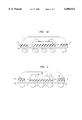
- FIG. 2 shows a semiconductor package with moisture vents according to another embodiment of the present invention.
- the package includes an external circuit element 120, such as a printed circuit board, having a first surface 122 with contact pads 124 and a second surface 126 including terminals 128.
- a moisture-permeable layer 130 substantially similar to that described above is formed atop the first surface 122 of the printed circuit board 120.
- the moisture-permeable layer 130 has a central region 154 in which the top surface 134 of the moisture-permeable layer 130 is substantially flat and parallel to the first surface 122 of the printed circuit board 120 and peripheral regions 156 in which the top surface 134 of the moisture-permeable layer extend up and away from the first surface 122 of the printed circuit board at an angle designated by the symbol theta.
- the moisture-permeable layer 130 is thicker at the peripheral regions 156, at the edges of the package, than at the central region 154 thereof. Maximizing the exterior surface area of the moisture-permeable layer at such edges, maximized the amount of moisture which can pass through the moisture-permeable layer.
- FIGS. 3A-3D show a method of manufacturing a semiconductor package with moisture vents in accordance with another preferred embodiment of the present invention. Certain steps of the method are disclosed in commonly assigned, copending U.S. patent application Ser. No. 08/634,464, filed Apr. 18, 1996, the disclosure of which is hereby incorporated by reference herein.
- a sacrificial layer 220 has a first surface 222 and a second surface 226.
- the sacrificial layer 220 preferably includes a conductive metallic material, such as copper, aluminum, steel, iron, bronze or brass.
- the sacrificial layer 220 includes a sheet of copper having a substantially uniform thickness of about between 100 to 200 microns. However, the sacrificial layer 220 may be thicker or thinner in other embodiments.
- a moisture-permeable layer 230 is provided over the first surface 222 of the copper sheet 220.
- the moisture-permeable layer 230 includes one or more openings 232 therein so that wire bonds may be electrically interconnected with the copper sheet 220 as will be described in more detail below.
- a semiconductor chip 236 having a rear surface 238 and a front face 240 including contacts 242 is next juxtaposed with the top surface 234 of the moisture-permeable layer 230, and the rear surface of the chip 236 is assembled with the top surface 234 of the moisture-permeable layer 230.
- the chip contacts 242 are then electrically interconnected with the copper sheet 220 by using wire bonding techniques whereby conductive wires 244 have first ends 246 connected to the chip contacts 242 and second ends 248 connected to the copper sheet 220.
- a curable moisture-impermeable encapsulant 250 such as an epoxy, is provided over the top of the assembly so as to encapsulate the semiconductor chip 236 and the wire bonds 244.
- conductive terminals 228 are formed at the bottom surface of the semiconductor package by selectively removing portions of the copper sheet 220.
- selected portions of the copper sheet 220 are etched away to leave the conductive terminals 228 accessible at a bottom surface 226 of the assembly. Removing selected portions of copper layer 220 provides additional outlets for moisture venting.
- the chip package may be electrically connected to an external circuit element, such as a printed circuit board, by using solder balls or other conductive elements.
- moisture-permeable layer 230 extends to the edges of the package. However, because the moisture-permeable layer 230 is exposed at the bottom face of the package, the moisture-permeable layer can provide a vent for moisture, even if it does not extend to the edges of the package.
- FIGS. 4A-4C show yet another embodiment of a semiconductor package with moisture vents.
- FIG. 4A shows a top view of a printed circuit board 320, having a first surface 322 and one or more contact pads 324 on the first surface 322 thereof.
- a moisture-permeable layer 330 is formed over the first surface 322 of the printed circuit board 320.
- the configuration of the moisture-permeable layer 330 may be modified so that it does not completely cover the top surface 322 of the printed circuit board 320 because it may not be necessary for the moisture-permeable layer to be present at the entire periphery of the package.
- FIG. 4A shows a top view of a printed circuit board 320, having a first surface 322 and one or more contact pads 324 on the first surface 322 thereof.
- a moisture-permeable layer 330 is formed over the first surface 322 of the printed circuit board 320.
- the configuration of the moisture-permeable layer 330 may be modified so that it does not completely cover the top surface
- the moisture-permeable layer is in the shape of a cross and has four projections which extend to the four edges of the printed circuit board 320, however, the moisture-permeable layer 330 does not cover the corners 354 of the printed circuit board 320. In other words, the moisture-permeable layer only has to be present at one or more exposed surfaces of the package to provide a sufficient outlet for moisture trapped within the package.
- the moisture-permeable layer 330 preferably includes openings 332 therein which are in alignment with the contact pads 324 of the substrate so that the contact pads 324 are accessible through the moisture-permeable layer 330.
- a semiconductor chip 336 having one or more contacts 342 on a front face 340 thereof is juxtaposed with the moisture-permeable layer 330, and the rear surface (not shown) of the chip 336 is assembled to the top surface of the moisture-permeable layer.
- the chip contacts 342 are electrically interconnected with the contact pads 324 of the printed circuit board 320 by using wire bonding techniques, whereby wire bonds 344 have first ends 346 connected to the chip contacts 342 and second ends 348 connected to the contact pads 324.
- a moisture-impermeable encapsulant 250 similar in composition to that described above, is then provided over the top surface of the substrate, the moisture-permeable layer, the chip and the wire bonds.
- the moisture-impermeable encapsulant 250 preferably extends to the four corners of the substrate and serves to "lock-down" the chip on the substrate, as disclosed in the above-mentioned '464 patent application, the disclosure of which is hereby incorporated by reference herein.
- the embodiment shown in FIGS. 4A-4C shows the moisture-permeable layer 330 extending to all four edges of the package, in other embodiments, the compliant layer may only extend to one, two or three edges.
- the thickness of the moisture-permeable layer 330 in the vicinity of the edge may be increased to provide more surface area at the exterior edge of the moisture-permeable layer to enhance moisture venting through the moisture-permeable layer.
- portions of circuit board 320 may be removed to expose regions of the moisture-permeable layer at the bottom surface of the package.
- FIGS. 5A-5D show another method of making a semiconductor package with moisture vents according to a further preferred embodiment of the present invention.
- a printed circuit board 420 such as a rigid printed circuit board or a flexible circuit board, is provided having a first surface 422 including conductive pads 424 and a second surface 426 including conductive terminals 428.
- the printed circuit board 420 typically includes internal circuitry (not shown) for electrically interconnecting one or more of the conductive pads 424 with one or more of the terminals 428.
- the printed circuit board 420 includes one or more apertures 470 extending through the width of the board 420 from the first surface 422 to the second surface 426 thereof.
- the apertures 470 are preferably positioned in one or more corners or edges of the printed circuit board 420.
- a moisture-permeable compliant layer 430 comprising materials substantially similar to those described above, is provided over the first surface 422 of the printed circuit board 420.
- the moisture-permeable layer is substantially continuous and extends to one or more edges of the printed circuit board so that one or more peripheral edges of the moisture-permeable layer are exposed at an exterior surface of the package.
- the moisture-permeable layer 430 includes first set of apertures 432 which are preferably in alignment with the contact pads 424 so that the contact pads 424 are accessible at a top surface 434 of the moisture-permeable layer 430.
- the moisture-permeable layer 430 also includes a second set of apertures 472 overlying the one or more apertures 470 extending through the printed circuit board 420.
- a microelectronic element 436 such as a semiconductor chip, having a rear surface 438 and a front face 440 including contacts 442 is juxtaposed with the top surface 434 of the moisture-permeable layer 430.
- the rear surface 438 of the microelectronic element 436 is then secured over the top surface 434 of the moisture-permeable layer 430.
- the chip contacts 442 are electrically interconnected with the contact pads 424 on the printed circuit board 420 using flexible conductive elements 444, such as wire bonds, having first ends 446 connected to the chip contacts 442 and second ends 448 bonded to the contact pads 424 of the printed circuit board 420.
- FIG. 6 shows a top view of FIG. 5C illustrating the apertures 472/470 in one or more corners of the printed circuit board 420.
- the contacts 442 on the microelectronic element 436 are electrically connected to the contact pads 424 on the printed circuit board 420 via flexible conductive elements 444.
- the entire assembly is then encapsulated with a moisture-impermeable encapsulant 450.
- the encapsulant 450 preferably includes any curable dielectric material which allows little or no moisture to pass therethrough, such as an epoxy.
- an epoxy Such epoxy overmolding compounds are commonly used in the packaging industry and can be optimized to ensure high reliability of the flexible conductive elements, e.g. the compounds may allow for the movement or flexing of the wires.
- the epoxy overmolding my also be loaded with materials to bring the cured encapsulant's thermal coefficient of expansion ("TCE") closer to the CTE of the silicon chip.
- TCE thermal coefficient of expansion
- the encapsulant 450 is allowed to project through the respective aligned apertures 472 and 470 in the compliant layer 430 and the printed circuit board 420.
- the encapsulant 450 is allowed to flow laterally along the second surface 426 of the printed circuit board 420 so as to form enlarged heads or bumps 474 of encapsulant material 450 overlying the second surface 426 of the printed circuit board 420.
- the encapsulant 450 is then cured by heat, UV light, chemical curing or radiation. Once the encapsulant 450 has been cured, the projections or bumps 474 serve to reliably secure or "lock-down" the moisture-permeable layer 430 over the first surface 422 of the printed circuit board 420.
- the moisture-permeable layer 430 at the periphery of the package serves as a moisture vent for the assembly. As such, any moisture present in the package will pass laterally through the moisture-permeable layer 430 and out the sides of the package assembly.
- the conductive terminals may have a "rivet-like" shape.
- FIG. 7A shows a sacrificial layer 520 having a first surface 522 and a second surface 526.
- the sacrificial layer 520 may include a conductive metallic material, a polymer material or a combination of both.
- a moisture-permeable compliant layer 530 such as that described above, is disposed on top of the first surface 522 of the sacrificial layer 520.
- the moisture-permeable layer 530 includes apertures 532 which may be developed and removed using standard photolithographic techniques so as to control the creation and placement of the apertures.
- the moisture-permeable layer 530 initially serves as an etching mask and a plurality of cavities 525 are removed from the first surface 522 of the sacrificial layer 520.
- the sacrificial layer 520 preferably includes an etchable layer so that the cavities 525 may simply be etched into the sacrificial layer 520 in the form desired.
- conductive terminals 528 are next plated into the cavities 525 and apertures 532 in the compliant layer 530 so as to create rivet-like terminals.
- These terminals 528 have a central post 527 extending through the aperture 532 in the compliant layer 530, a bottom bump flange 529 at a lower end of the central post 527 and a top bump flange 531 at an upper end of the central post 527. Both bump flanges have flange areas which extend beyond the diameter of the central post.
- FIGS. 7F and 7G show alternate cross-sectional terminal configurations, according to the present invention. In the embodiment shown in FIG.
- the terminal 528 includes top bump flange 531, central post 527 extending through the aperture in the compliant layer 530 and bottom bump flange 529.
- the bump flanges 531' and 529' are more squared-off at the edges, as compared to the rounded/oval bump flanges described above. Bump flanges having other shapes may also be used.
- a semiconductor chip 536 having contacts 542 on a front face 540 thereof is then back-bonded to the first surface 534 of the compliant layer 530 and electrically connected to the terminals 528 using flexible wire bonds 544, as described above in the earlier embodiments.
- the chip 536, moisture-permeable layer 530, terminals 528 and wires 544 are then encapsulated as described above.
- the sacrificial layer 520 is then etched away to leave the conductive terminals 528 accessible at the bottom of the package.
- moisture-permeable layer 530 extends to the edges of the package. However, because the moisture-permeable layer 530 is exposed at the bottom face of the package, the permeable compliant layer can provide a vent for moisture, even if it does not extend to the edges of the package.
- the terminals 628 extend all the way through a substrate 620, such as a printed circuit board.
- the substrate 620 is not etched away, as shown above in FIGS. 7D and 7E, but is left in place.
- the substrate 620 enhances the structural integrity of the final assembly.
- the moisture-permeable layer 630 at the periphery of the package serves as a moisture vent for the assembly. As such, any moisture present in the package will pass laterally through the moisture-permeable layer 630 and out the sides of the package assembly.
- any of the package assemblies described above may be manufactured using single semiconductor chips or may be manufactured on a wafer-scale whereby individual packaged chips or packaged multi-chip modules are diced from the wafer after completing the assembly process.
- any of the package assemblies described above may be manufactured using single semiconductor chips or may be manufactured on a wafer-scale whereby individual packaged chips or packaged multi-chip modules are diced from the wafer after completing the assembly process.
Abstract
Description
Claims (25)
Priority Applications (2)
| Application Number | Priority Date | Filing Date | Title |
|---|---|---|---|
| US09/059,662 US6080932A (en) | 1998-04-14 | 1998-04-14 | Semiconductor package assemblies with moisture vents |
| US09/561,727 US6358780B1 (en) | 1998-04-14 | 2000-05-01 | Semiconductor package assemblies with moisture vents and methods of making same |
Applications Claiming Priority (1)
| Application Number | Priority Date | Filing Date | Title |
|---|---|---|---|
| US09/059,662 US6080932A (en) | 1998-04-14 | 1998-04-14 | Semiconductor package assemblies with moisture vents |
Related Child Applications (1)
| Application Number | Title | Priority Date | Filing Date |
|---|---|---|---|
| US09/561,727 Division US6358780B1 (en) | 1998-04-14 | 2000-05-01 | Semiconductor package assemblies with moisture vents and methods of making same |
Publications (1)
| Publication Number | Publication Date |
|---|---|
| US6080932A true US6080932A (en) | 2000-06-27 |
Family
ID=22024420
Family Applications (2)
| Application Number | Title | Priority Date | Filing Date |
|---|---|---|---|
| US09/059,662 Expired - Lifetime US6080932A (en) | 1998-04-14 | 1998-04-14 | Semiconductor package assemblies with moisture vents |
| US09/561,727 Expired - Lifetime US6358780B1 (en) | 1998-04-14 | 2000-05-01 | Semiconductor package assemblies with moisture vents and methods of making same |
Family Applications After (1)
| Application Number | Title | Priority Date | Filing Date |
|---|---|---|---|
| US09/561,727 Expired - Lifetime US6358780B1 (en) | 1998-04-14 | 2000-05-01 | Semiconductor package assemblies with moisture vents and methods of making same |
Country Status (1)
| Country | Link |
|---|---|
| US (2) | US6080932A (en) |
Cited By (84)
| Publication number | Priority date | Publication date | Assignee | Title |
|---|---|---|---|---|
| US6208524B1 (en) * | 1998-07-23 | 2001-03-27 | Micron Technology, Inc. | Electronic apparatus, battery powerable apparatus, and radio frequency communication device |
| US6339261B1 (en) * | 1999-04-06 | 2002-01-15 | Shinko Electric Industries Co., Ltd. | Semiconductor device and process of producing same |
| US6340793B1 (en) * | 1999-03-17 | 2002-01-22 | Hitachi, Ltd. | Semiconductor device |
| US20020125562A1 (en) * | 2000-03-27 | 2002-09-12 | Crowley Sean T. | Attaching semiconductor dies to substrates with conductive straps |
| US20020187590A1 (en) * | 2000-08-31 | 2002-12-12 | Micron Technology, Inc. | Ball grid array packages with thermally conductive containers |
| US20030029633A1 (en) * | 2000-08-23 | 2003-02-13 | Ahmad Syed Sajid | Interconnecting substrates for electrical coupling of microelectronic components |
| US20030102538A1 (en) * | 2000-06-27 | 2003-06-05 | Stefan Paulus | Leadframe for semiconductor chips and electronic devices and production methods for a leadframe and for electronic devices |
| US20030197255A1 (en) * | 2001-09-20 | 2003-10-23 | Mitsubishi Denki Kabushiki Kaisha | Semiconductor device |
| US20030201526A1 (en) * | 1999-11-23 | 2003-10-30 | Bolken Todd O. | Packages for semiconductor die |
| US6768646B1 (en) | 1998-01-23 | 2004-07-27 | Texas Instruments Incorporated | High density internal ball grid array integrated circuit package |
| US6791171B2 (en) | 2000-06-20 | 2004-09-14 | Nanonexus, Inc. | Systems for testing and packaging integrated circuits |
| US20050026476A1 (en) * | 2000-06-20 | 2005-02-03 | Sammy Mok | Systems for testing and packaging integrated circuits |
| US20050224936A1 (en) * | 2004-04-12 | 2005-10-13 | Jeng-Dah Wu | Chip package structure |
| WO2007075789A1 (en) * | 2005-12-27 | 2007-07-05 | Tessera, Inc. | Compliant terminal mountings with vented spaces and methods |
| US20090004784A1 (en) * | 2003-01-21 | 2009-01-01 | Siliconware Precision Industries Co., Ltd. | Method for fabricating semiconductor package free of substrate |
| US20090242268A1 (en) * | 2008-03-31 | 2009-10-01 | Nec Electronics Corporation | Semiconductor device capable of switching operation modes |
| US7772860B2 (en) | 1999-05-27 | 2010-08-10 | Nanonexus, Inc. | Massively parallel interface for electronic circuit |
| US20100289132A1 (en) * | 2009-05-13 | 2010-11-18 | Shih-Fu Huang | Substrate having embedded single patterned metal layer, and package applied with the same, and methods of manufacturing of the substrate and package |
| US20100288541A1 (en) * | 2009-05-13 | 2010-11-18 | Advanced Semiconductor Engineering, Inc. | Substrate having single patterned metal layer, and package applied with the substrate , and methods of manufacturing of the substrate and package |
| WO2010141266A1 (en) * | 2009-06-02 | 2010-12-09 | Hsio Technologies, Llc | Compliant printed circuit peripheral lead semiconductor package |
| US20100314744A1 (en) * | 2009-05-13 | 2010-12-16 | Shih-Fu Huang | Substrate having single patterned metal layer exposing patterned dielectric layer, chip package structure including the substrate, and manufacturing methods thereof |
| US20100320610A1 (en) * | 2009-05-13 | 2010-12-23 | Shih-Fu Huang | Semiconductor package with substrate having single metal layer and manufacturing methods thereof |
| US20100320593A1 (en) * | 2009-06-19 | 2010-12-23 | Advanced Semiconductor Engineering, Inc. | Chip Package Structure and Manufacturing Methods Thereof |
| US7872482B2 (en) | 2000-05-23 | 2011-01-18 | Verigy (Singapore) Pte. Ltd | High density interconnect system having rapid fabrication cycle |
| US20110018124A1 (en) * | 2009-07-23 | 2011-01-27 | Advanced Semiconductor Engineering, Inc. | Semiconductor Device Packages, Redistribution Structures, and Manufacturing Methods Thereof |
| US20110018118A1 (en) * | 2009-07-21 | 2011-01-27 | Advanced Semiconductor Engineering, Inc. | Semiconductor Device Packages, Redistribution Structures, and Manufacturing Methods Thereof |
| US20110057301A1 (en) * | 2009-09-08 | 2011-03-10 | Advanced Semiconductor Engineering, Inc. | Semiconductor package |
| US20110084370A1 (en) * | 2009-10-14 | 2011-04-14 | Advanced Semiconductor Engineering, Inc. | Semiconductor package and process for fabricating same |
| US7952373B2 (en) | 2000-05-23 | 2011-05-31 | Verigy (Singapore) Pte. Ltd. | Construction structures and manufacturing processes for integrated circuit wafer probe card assemblies |
| US20110177654A1 (en) * | 2010-01-21 | 2011-07-21 | Advanced Semiconductor Engineering, Inc. | Wafer-Level Semiconductor Device Packages with Three-Dimensional Fan-Out and Manufacturing Methods Thereof |
| US20110182042A1 (en) * | 2007-07-05 | 2011-07-28 | Occam Portfolio Llc | Electronic Assemblies without Solder and Methods for their Manufacture |
| US20110194265A1 (en) * | 2010-02-05 | 2011-08-11 | Advanced Semiconductor Engineering, Inc. | Embedded Component Substrate and Manufacturing Methods Thereof |
| US20110227220A1 (en) * | 2010-03-22 | 2011-09-22 | Chia-Ching Chen | Stackable semiconductor package and manufacturing method thereof |
| US8035213B2 (en) | 2007-10-22 | 2011-10-11 | Advanced Semiconductor Engineering, Inc. | Chip package structure and method of manufacturing the same |
| US20110296680A1 (en) * | 2010-06-05 | 2011-12-08 | Raytheon Company | Vent blocking on vented ball grid arrays to provide a cleaner solution barrier |
| US8278746B2 (en) | 2010-04-02 | 2012-10-02 | Advanced Semiconductor Engineering, Inc. | Semiconductor device packages including connecting elements |
| US8378466B2 (en) | 2009-11-19 | 2013-02-19 | Advanced Semiconductor Engineering, Inc. | Wafer-level semiconductor device packages with electromagnetic interference shielding |
| US8525346B2 (en) | 2009-06-02 | 2013-09-03 | Hsio Technologies, Llc | Compliant conductive nano-particle electrical interconnect |
| US8569894B2 (en) | 2010-01-13 | 2013-10-29 | Advanced Semiconductor Engineering, Inc. | Semiconductor package with single sided substrate design and manufacturing methods thereof |
| US8610265B2 (en) | 2009-06-02 | 2013-12-17 | Hsio Technologies, Llc | Compliant core peripheral lead semiconductor test socket |
| US8618649B2 (en) | 2009-06-02 | 2013-12-31 | Hsio Technologies, Llc | Compliant printed circuit semiconductor package |
| US8624374B2 (en) | 2010-04-02 | 2014-01-07 | Advanced Semiconductor Engineering, Inc. | Semiconductor device packages with fan-out and with connecting elements for stacking and manufacturing methods thereof |
| US8758067B2 (en) | 2010-06-03 | 2014-06-24 | Hsio Technologies, Llc | Selective metalization of electrical connector or socket housing |
| US8789272B2 (en) | 2009-06-02 | 2014-07-29 | Hsio Technologies, Llc | Method of making a compliant printed circuit peripheral lead semiconductor test socket |
| US8803539B2 (en) | 2009-06-03 | 2014-08-12 | Hsio Technologies, Llc | Compliant wafer level probe assembly |
| US8912812B2 (en) | 2009-06-02 | 2014-12-16 | Hsio Technologies, Llc | Compliant printed circuit wafer probe diagnostic tool |
| US8928344B2 (en) | 2009-06-02 | 2015-01-06 | Hsio Technologies, Llc | Compliant printed circuit socket diagnostic tool |
| US8941222B2 (en) | 2010-11-11 | 2015-01-27 | Advanced Semiconductor Engineering Inc. | Wafer level semiconductor package and manufacturing methods thereof |
| US8955215B2 (en) | 2009-05-28 | 2015-02-17 | Hsio Technologies, Llc | High performance surface mount electrical interconnect |
| US8970031B2 (en) | 2009-06-16 | 2015-03-03 | Hsio Technologies, Llc | Semiconductor die terminal |
| US8981809B2 (en) | 2009-06-29 | 2015-03-17 | Hsio Technologies, Llc | Compliant printed circuit semiconductor tester interface |
| US8981568B2 (en) | 2009-06-16 | 2015-03-17 | Hsio Technologies, Llc | Simulated wirebond semiconductor package |
| US8988093B2 (en) | 2009-06-02 | 2015-03-24 | Hsio Technologies, Llc | Bumped semiconductor wafer or die level electrical interconnect |
| US8987886B2 (en) | 2009-06-02 | 2015-03-24 | Hsio Technologies, Llc | Copper pillar full metal via electrical circuit structure |
| US8984748B2 (en) | 2009-06-29 | 2015-03-24 | Hsio Technologies, Llc | Singulated semiconductor device separable electrical interconnect |
| US9054097B2 (en) | 2009-06-02 | 2015-06-09 | Hsio Technologies, Llc | Compliant printed circuit area array semiconductor device package |
| US9093767B2 (en) | 2009-06-02 | 2015-07-28 | Hsio Technologies, Llc | High performance surface mount electrical interconnect |
| US9136196B2 (en) | 2009-06-02 | 2015-09-15 | Hsio Technologies, Llc | Compliant printed circuit wafer level semiconductor package |
| US9184527B2 (en) | 2009-06-02 | 2015-11-10 | Hsio Technologies, Llc | Electrical connector insulator housing |
| US9184145B2 (en) | 2009-06-02 | 2015-11-10 | Hsio Technologies, Llc | Semiconductor device package adapter |
| US9196980B2 (en) | 2009-06-02 | 2015-11-24 | Hsio Technologies, Llc | High performance surface mount electrical interconnect with external biased normal force loading |
| US9232654B2 (en) | 2009-06-02 | 2016-01-05 | Hsio Technologies, Llc | High performance electrical circuit structure |
| US9231328B2 (en) | 2009-06-02 | 2016-01-05 | Hsio Technologies, Llc | Resilient conductive electrical interconnect |
| US9276339B2 (en) | 2009-06-02 | 2016-03-01 | Hsio Technologies, Llc | Electrical interconnect IC device socket |
| US9276336B2 (en) | 2009-05-28 | 2016-03-01 | Hsio Technologies, Llc | Metalized pad to electrical contact interface |
| US9277654B2 (en) | 2009-06-02 | 2016-03-01 | Hsio Technologies, Llc | Composite polymer-metal electrical contacts |
| US9320144B2 (en) | 2009-06-17 | 2016-04-19 | Hsio Technologies, Llc | Method of forming a semiconductor socket |
| US9320133B2 (en) | 2009-06-02 | 2016-04-19 | Hsio Technologies, Llc | Electrical interconnect IC device socket |
| US9318862B2 (en) | 2009-06-02 | 2016-04-19 | Hsio Technologies, Llc | Method of making an electronic interconnect |
| US9350093B2 (en) | 2010-06-03 | 2016-05-24 | Hsio Technologies, Llc | Selective metalization of electrical connector or socket housing |
| US9406658B2 (en) | 2010-12-17 | 2016-08-02 | Advanced Semiconductor Engineering, Inc. | Embedded component device and manufacturing methods thereof |
| US9414500B2 (en) | 2009-06-02 | 2016-08-09 | Hsio Technologies, Llc | Compliant printed flexible circuit |
| US9536815B2 (en) | 2009-05-28 | 2017-01-03 | Hsio Technologies, Llc | Semiconductor socket with direct selective metalization |
| US9559447B2 (en) | 2015-03-18 | 2017-01-31 | Hsio Technologies, Llc | Mechanical contact retention within an electrical connector |
| US9564346B2 (en) | 2009-10-14 | 2017-02-07 | Advanced Semiconductor Engineering, Inc. | Package carrier, semiconductor package, and process for fabricating same |
| US9603249B2 (en) | 2009-06-02 | 2017-03-21 | Hsio Technologies, Llc | Direct metalization of electrical circuit structures |
| US9613841B2 (en) | 2009-06-02 | 2017-04-04 | Hsio Technologies, Llc | Area array semiconductor device package interconnect structure with optional package-to-package or flexible circuit to package connection |
| US9689897B2 (en) | 2010-06-03 | 2017-06-27 | Hsio Technologies, Llc | Performance enhanced semiconductor socket |
| US9699906B2 (en) | 2009-06-02 | 2017-07-04 | Hsio Technologies, Llc | Hybrid printed circuit assembly with low density main core and embedded high density circuit regions |
| US9761520B2 (en) | 2012-07-10 | 2017-09-12 | Hsio Technologies, Llc | Method of making an electrical connector having electrodeposited terminals |
| US9930775B2 (en) | 2009-06-02 | 2018-03-27 | Hsio Technologies, Llc | Copper pillar full metal via electrical circuit structure |
| US10159154B2 (en) | 2010-06-03 | 2018-12-18 | Hsio Technologies, Llc | Fusion bonded liquid crystal polymer circuit structure |
| US10506722B2 (en) | 2013-07-11 | 2019-12-10 | Hsio Technologies, Llc | Fusion bonded liquid crystal polymer electrical circuit structure |
| US10667410B2 (en) | 2013-07-11 | 2020-05-26 | Hsio Technologies, Llc | Method of making a fusion bonded circuit structure |
Families Citing this family (7)
| Publication number | Priority date | Publication date | Assignee | Title |
|---|---|---|---|---|
| JP3679687B2 (en) * | 2000-06-08 | 2005-08-03 | 三洋電機株式会社 | Hybrid integrated circuit device |
| US7498196B2 (en) * | 2001-03-30 | 2009-03-03 | Megica Corporation | Structure and manufacturing method of chip scale package |
| US6773964B2 (en) * | 2002-09-30 | 2004-08-10 | Koninklijke Philips Electronics N.V. | Integrated circuit package including sealed gaps and prevention of vapor induced failures and method of manufacturing the same |
| US20040262781A1 (en) * | 2003-06-27 | 2004-12-30 | Semiconductor Components Industries, Llc | Method for forming an encapsulated device and structure |
| TWI497679B (en) * | 2009-11-27 | 2015-08-21 | Advanced Semiconductor Eng | Semiconductor package and manufacturing method thereof |
| US20130234330A1 (en) * | 2012-03-08 | 2013-09-12 | Infineon Technologies Ag | Semiconductor Packages and Methods of Formation Thereof |
| US9220183B1 (en) * | 2014-07-16 | 2015-12-22 | International Business Machines Corporation | Devices employing semiconductor die having hydrophobic coatings, and related cooling methods |
Citations (15)
| Publication number | Priority date | Publication date | Assignee | Title |
|---|---|---|---|---|
| US3837067A (en) * | 1971-12-23 | 1974-09-24 | Bunker Ramo | Method of making integrated circuit package |
| US4866506A (en) * | 1984-04-02 | 1989-09-12 | Oki Electric Industry Co., Ltd. | Plastic-sealed IC device of heat-resistant construction |
| US5108784A (en) * | 1987-12-16 | 1992-04-28 | Ford Motor Company | Composite polymer/desiccant coatings for IC encapsulation |
| US5148266A (en) * | 1990-09-24 | 1992-09-15 | Ist Associates, Inc. | Semiconductor chip assemblies having interposer and flexible lead |
| US5148265A (en) * | 1990-09-24 | 1992-09-15 | Ist Associates, Inc. | Semiconductor chip assemblies with fan-in leads |
| US5296738A (en) * | 1991-07-08 | 1994-03-22 | Motorola, Inc. | Moisture relief for chip carrier |
| US5446315A (en) * | 1991-03-08 | 1995-08-29 | Japan Gore-Tex, Inc. | Resin-sealed semiconductor device containing porous fluorocarbon resin |
| US5548087A (en) * | 1993-05-07 | 1996-08-20 | At&T Corp. | Molded plastic packaging of electronic devices |
| US5557150A (en) * | 1992-02-07 | 1996-09-17 | Lsi Logic Corporation | Overmolded semiconductor package |
| US5679977A (en) * | 1990-09-24 | 1997-10-21 | Tessera, Inc. | Semiconductor chip assemblies, methods of making same and components for same |
| US5721450A (en) * | 1995-06-12 | 1998-02-24 | Motorola, Inc. | Moisture relief for chip carriers |
| US5742007A (en) * | 1996-08-05 | 1998-04-21 | Motorola, Inc. | Electronic device package and method for forming the same |
| US5767446A (en) * | 1995-10-27 | 1998-06-16 | Anam Industrial Co., Ltd. | Printed circuit board having epoxy barrier around a throughout slot and ball grid array semiconductor package |
| US5796038A (en) * | 1997-06-16 | 1998-08-18 | Vlsi Technology, Inc. | Technique to produce cavity-up HBGA packages |
| US5949141A (en) * | 1995-12-22 | 1999-09-07 | Micron Technology, Inc. | Laminated film/metal structures |
Family Cites Families (3)
| Publication number | Priority date | Publication date | Assignee | Title |
|---|---|---|---|---|
| TW347149U (en) * | 1993-02-26 | 1998-12-01 | Dow Corning | Integrated circuits protected from the environment by ceramic and barrier metal layers |
| US5474958A (en) * | 1993-05-04 | 1995-12-12 | Motorola, Inc. | Method for making semiconductor device having no die supporting surface |
| US5733800A (en) * | 1996-05-21 | 1998-03-31 | Micron Technology, Inc. | Underfill coating for LOC package |
-
1998
- 1998-04-14 US US09/059,662 patent/US6080932A/en not_active Expired - Lifetime
-
2000
- 2000-05-01 US US09/561,727 patent/US6358780B1/en not_active Expired - Lifetime
Patent Citations (15)
| Publication number | Priority date | Publication date | Assignee | Title |
|---|---|---|---|---|
| US3837067A (en) * | 1971-12-23 | 1974-09-24 | Bunker Ramo | Method of making integrated circuit package |
| US4866506A (en) * | 1984-04-02 | 1989-09-12 | Oki Electric Industry Co., Ltd. | Plastic-sealed IC device of heat-resistant construction |
| US5108784A (en) * | 1987-12-16 | 1992-04-28 | Ford Motor Company | Composite polymer/desiccant coatings for IC encapsulation |
| US5679977A (en) * | 1990-09-24 | 1997-10-21 | Tessera, Inc. | Semiconductor chip assemblies, methods of making same and components for same |
| US5148265A (en) * | 1990-09-24 | 1992-09-15 | Ist Associates, Inc. | Semiconductor chip assemblies with fan-in leads |
| US5148266A (en) * | 1990-09-24 | 1992-09-15 | Ist Associates, Inc. | Semiconductor chip assemblies having interposer and flexible lead |
| US5446315A (en) * | 1991-03-08 | 1995-08-29 | Japan Gore-Tex, Inc. | Resin-sealed semiconductor device containing porous fluorocarbon resin |
| US5296738A (en) * | 1991-07-08 | 1994-03-22 | Motorola, Inc. | Moisture relief for chip carrier |
| US5557150A (en) * | 1992-02-07 | 1996-09-17 | Lsi Logic Corporation | Overmolded semiconductor package |
| US5548087A (en) * | 1993-05-07 | 1996-08-20 | At&T Corp. | Molded plastic packaging of electronic devices |
| US5721450A (en) * | 1995-06-12 | 1998-02-24 | Motorola, Inc. | Moisture relief for chip carriers |
| US5767446A (en) * | 1995-10-27 | 1998-06-16 | Anam Industrial Co., Ltd. | Printed circuit board having epoxy barrier around a throughout slot and ball grid array semiconductor package |
| US5949141A (en) * | 1995-12-22 | 1999-09-07 | Micron Technology, Inc. | Laminated film/metal structures |
| US5742007A (en) * | 1996-08-05 | 1998-04-21 | Motorola, Inc. | Electronic device package and method for forming the same |
| US5796038A (en) * | 1997-06-16 | 1998-08-18 | Vlsi Technology, Inc. | Technique to produce cavity-up HBGA packages |
Cited By (130)
| Publication number | Priority date | Publication date | Assignee | Title |
|---|---|---|---|---|
| US6768646B1 (en) | 1998-01-23 | 2004-07-27 | Texas Instruments Incorporated | High density internal ball grid array integrated circuit package |
| US6208524B1 (en) * | 1998-07-23 | 2001-03-27 | Micron Technology, Inc. | Electronic apparatus, battery powerable apparatus, and radio frequency communication device |
| US6512176B2 (en) | 1999-03-17 | 2003-01-28 | Hitachi, Ltd. | Semiconductor device |
| US6340793B1 (en) * | 1999-03-17 | 2002-01-22 | Hitachi, Ltd. | Semiconductor device |
| US6339261B1 (en) * | 1999-04-06 | 2002-01-15 | Shinko Electric Industries Co., Ltd. | Semiconductor device and process of producing same |
| US7772860B2 (en) | 1999-05-27 | 2010-08-10 | Nanonexus, Inc. | Massively parallel interface for electronic circuit |
| US7884634B2 (en) | 1999-05-27 | 2011-02-08 | Verigy (Singapore) Pte, Ltd | High density interconnect system having rapid fabrication cycle |
| US20040119173A1 (en) * | 1999-11-23 | 2004-06-24 | Bolken Todd O | Packages for semiconductor die |
| US7091060B2 (en) * | 1999-11-23 | 2006-08-15 | Micron Technology, Inc. | Circuit and substrate encapsulation methods |
| US20030201526A1 (en) * | 1999-11-23 | 2003-10-30 | Bolken Todd O. | Packages for semiconductor die |
| US7144245B2 (en) | 1999-11-23 | 2006-12-05 | Micron Technology, Inc. | Packages for semiconductor die |
| US7239029B2 (en) | 1999-11-23 | 2007-07-03 | Micron Technology, Inc. | Packages for semiconductor die |
| US20020125562A1 (en) * | 2000-03-27 | 2002-09-12 | Crowley Sean T. | Attaching semiconductor dies to substrates with conductive straps |
| US7952373B2 (en) | 2000-05-23 | 2011-05-31 | Verigy (Singapore) Pte. Ltd. | Construction structures and manufacturing processes for integrated circuit wafer probe card assemblies |
| US7872482B2 (en) | 2000-05-23 | 2011-01-18 | Verigy (Singapore) Pte. Ltd | High density interconnect system having rapid fabrication cycle |
| US20050026476A1 (en) * | 2000-06-20 | 2005-02-03 | Sammy Mok | Systems for testing and packaging integrated circuits |
| US6791171B2 (en) | 2000-06-20 | 2004-09-14 | Nanonexus, Inc. | Systems for testing and packaging integrated circuits |
| US20060240690A9 (en) * | 2000-06-20 | 2006-10-26 | Sammy Mok | Systems for testing and packaging integrated circuits |
| US7247035B2 (en) | 2000-06-20 | 2007-07-24 | Nanonexus, Inc. | Enhanced stress metal spring contactor |
| US20030102538A1 (en) * | 2000-06-27 | 2003-06-05 | Stefan Paulus | Leadframe for semiconductor chips and electronic devices and production methods for a leadframe and for electronic devices |
| US6969905B2 (en) * | 2000-06-27 | 2005-11-29 | Infineon Technologies Ag | Leadframe for semiconductor chips and electronic devices and production methods for a leadframe and for electronic devices |
| US20030029633A1 (en) * | 2000-08-23 | 2003-02-13 | Ahmad Syed Sajid | Interconnecting substrates for electrical coupling of microelectronic components |
| US6983551B2 (en) | 2000-08-23 | 2006-01-10 | Micron Technology, Inc. | Interconnecting substrates for electrical coupling of microelectronic components |
| US6982386B2 (en) * | 2000-08-23 | 2006-01-03 | Micron Technology, Inc. | Interconnecting substrates for electrical coupling of microelectronic components |
| US20030106709A1 (en) * | 2000-08-23 | 2003-06-12 | Ahmad Syed Sajid | Interconnecting substrates for electrical coupling of microelectronic components |
| US7399657B2 (en) | 2000-08-31 | 2008-07-15 | Micron Technology, Inc. | Ball grid array packages with thermally conductive containers |
| US20020187590A1 (en) * | 2000-08-31 | 2002-12-12 | Micron Technology, Inc. | Ball grid array packages with thermally conductive containers |
| US20030197255A1 (en) * | 2001-09-20 | 2003-10-23 | Mitsubishi Denki Kabushiki Kaisha | Semiconductor device |
| US6867484B2 (en) * | 2001-09-20 | 2005-03-15 | Mitsubishi Denki Kabushiki Kaisha | Semiconductor device |
| US20090004784A1 (en) * | 2003-01-21 | 2009-01-01 | Siliconware Precision Industries Co., Ltd. | Method for fabricating semiconductor package free of substrate |
| US7816187B2 (en) * | 2003-01-21 | 2010-10-19 | Siliconware Precision Industries Co., Ltd. | Method for fabricating semiconductor package free of substrate |
| US20050224936A1 (en) * | 2004-04-12 | 2005-10-13 | Jeng-Dah Wu | Chip package structure |
| WO2007075789A1 (en) * | 2005-12-27 | 2007-07-05 | Tessera, Inc. | Compliant terminal mountings with vented spaces and methods |
| CN101351884B (en) * | 2005-12-27 | 2010-10-27 | 泰塞拉公司 | Compliant terminal mountings with vented spaces and methods |
| US20110182042A1 (en) * | 2007-07-05 | 2011-07-28 | Occam Portfolio Llc | Electronic Assemblies without Solder and Methods for their Manufacture |
| US8035213B2 (en) | 2007-10-22 | 2011-10-11 | Advanced Semiconductor Engineering, Inc. | Chip package structure and method of manufacturing the same |
| US8633407B2 (en) | 2008-03-31 | 2014-01-21 | Renesas Electronics Corporation | Semiconductor device capable of switching operation modes |
| US7994437B2 (en) | 2008-03-31 | 2011-08-09 | Renesas Electronics Corporation | Semiconductor device capable of switching operation modes |
| US20090242268A1 (en) * | 2008-03-31 | 2009-10-01 | Nec Electronics Corporation | Semiconductor device capable of switching operation modes |
| US8344269B2 (en) | 2008-03-31 | 2013-01-01 | Renesas Electronics Corporation | Semiconductor device capable of switching operation modes |
| US7763812B2 (en) * | 2008-03-31 | 2010-07-27 | Nec Electronics Corporation | Semiconductor device capable of switching operation modes |
| US20100314744A1 (en) * | 2009-05-13 | 2010-12-16 | Shih-Fu Huang | Substrate having single patterned metal layer exposing patterned dielectric layer, chip package structure including the substrate, and manufacturing methods thereof |
| US20100320610A1 (en) * | 2009-05-13 | 2010-12-23 | Shih-Fu Huang | Semiconductor package with substrate having single metal layer and manufacturing methods thereof |
| US20100288541A1 (en) * | 2009-05-13 | 2010-11-18 | Advanced Semiconductor Engineering, Inc. | Substrate having single patterned metal layer, and package applied with the substrate , and methods of manufacturing of the substrate and package |
| US8367473B2 (en) | 2009-05-13 | 2013-02-05 | Advanced Semiconductor Engineering, Inc. | Substrate having single patterned metal layer exposing patterned dielectric layer, chip package structure including the substrate, and manufacturing methods thereof |
| US8288869B2 (en) | 2009-05-13 | 2012-10-16 | Advanced Semiconductor Engineering, Inc. | Semiconductor package with substrate having single metal layer and manufacturing methods thereof |
| US20100289132A1 (en) * | 2009-05-13 | 2010-11-18 | Shih-Fu Huang | Substrate having embedded single patterned metal layer, and package applied with the same, and methods of manufacturing of the substrate and package |
| US8399776B2 (en) | 2009-05-13 | 2013-03-19 | Advanced Semiconductor Engineering, Inc. | Substrate having single patterned metal layer, and package applied with the substrate , and methods of manufacturing of the substrate and package |
| US9276336B2 (en) | 2009-05-28 | 2016-03-01 | Hsio Technologies, Llc | Metalized pad to electrical contact interface |
| US8955215B2 (en) | 2009-05-28 | 2015-02-17 | Hsio Technologies, Llc | High performance surface mount electrical interconnect |
| US9660368B2 (en) | 2009-05-28 | 2017-05-23 | Hsio Technologies, Llc | High performance surface mount electrical interconnect |
| US9536815B2 (en) | 2009-05-28 | 2017-01-03 | Hsio Technologies, Llc | Semiconductor socket with direct selective metalization |
| US9184145B2 (en) | 2009-06-02 | 2015-11-10 | Hsio Technologies, Llc | Semiconductor device package adapter |
| US9276339B2 (en) | 2009-06-02 | 2016-03-01 | Hsio Technologies, Llc | Electrical interconnect IC device socket |
| US9184527B2 (en) | 2009-06-02 | 2015-11-10 | Hsio Technologies, Llc | Electrical connector insulator housing |
| US10609819B2 (en) | 2009-06-02 | 2020-03-31 | Hsio Technologies, Llc | Hybrid printed circuit assembly with low density main core and embedded high density circuit regions |
| US9930775B2 (en) | 2009-06-02 | 2018-03-27 | Hsio Technologies, Llc | Copper pillar full metal via electrical circuit structure |
| US9699906B2 (en) | 2009-06-02 | 2017-07-04 | Hsio Technologies, Llc | Hybrid printed circuit assembly with low density main core and embedded high density circuit regions |
| US9196980B2 (en) | 2009-06-02 | 2015-11-24 | Hsio Technologies, Llc | High performance surface mount electrical interconnect with external biased normal force loading |
| WO2010141266A1 (en) * | 2009-06-02 | 2010-12-09 | Hsio Technologies, Llc | Compliant printed circuit peripheral lead semiconductor package |
| US9136196B2 (en) | 2009-06-02 | 2015-09-15 | Hsio Technologies, Llc | Compliant printed circuit wafer level semiconductor package |
| US9613841B2 (en) | 2009-06-02 | 2017-04-04 | Hsio Technologies, Llc | Area array semiconductor device package interconnect structure with optional package-to-package or flexible circuit to package connection |
| US9603249B2 (en) | 2009-06-02 | 2017-03-21 | Hsio Technologies, Llc | Direct metalization of electrical circuit structures |
| US9093767B2 (en) | 2009-06-02 | 2015-07-28 | Hsio Technologies, Llc | High performance surface mount electrical interconnect |
| US9414500B2 (en) | 2009-06-02 | 2016-08-09 | Hsio Technologies, Llc | Compliant printed flexible circuit |
| US9318862B2 (en) | 2009-06-02 | 2016-04-19 | Hsio Technologies, Llc | Method of making an electronic interconnect |
| US9320133B2 (en) | 2009-06-02 | 2016-04-19 | Hsio Technologies, Llc | Electrical interconnect IC device socket |
| US8525346B2 (en) | 2009-06-02 | 2013-09-03 | Hsio Technologies, Llc | Compliant conductive nano-particle electrical interconnect |
| US9076884B2 (en) | 2009-06-02 | 2015-07-07 | Hsio Technologies, Llc | Compliant printed circuit semiconductor package |
| US8610265B2 (en) | 2009-06-02 | 2013-12-17 | Hsio Technologies, Llc | Compliant core peripheral lead semiconductor test socket |
| US8618649B2 (en) | 2009-06-02 | 2013-12-31 | Hsio Technologies, Llc | Compliant printed circuit semiconductor package |
| US9277654B2 (en) | 2009-06-02 | 2016-03-01 | Hsio Technologies, Llc | Composite polymer-metal electrical contacts |
| US9054097B2 (en) | 2009-06-02 | 2015-06-09 | Hsio Technologies, Llc | Compliant printed circuit area array semiconductor device package |
| US8704377B2 (en) | 2009-06-02 | 2014-04-22 | Hsio Technologies, Llc | Compliant conductive nano-particle electrical interconnect |
| US8987886B2 (en) | 2009-06-02 | 2015-03-24 | Hsio Technologies, Llc | Copper pillar full metal via electrical circuit structure |
| US8988093B2 (en) | 2009-06-02 | 2015-03-24 | Hsio Technologies, Llc | Bumped semiconductor wafer or die level electrical interconnect |
| US8789272B2 (en) | 2009-06-02 | 2014-07-29 | Hsio Technologies, Llc | Method of making a compliant printed circuit peripheral lead semiconductor test socket |
| US8955216B2 (en) | 2009-06-02 | 2015-02-17 | Hsio Technologies, Llc | Method of making a compliant printed circuit peripheral lead semiconductor package |
| US8829671B2 (en) | 2009-06-02 | 2014-09-09 | Hsio Technologies, Llc | Compliant core peripheral lead semiconductor socket |
| US9231328B2 (en) | 2009-06-02 | 2016-01-05 | Hsio Technologies, Llc | Resilient conductive electrical interconnect |
| US8912812B2 (en) | 2009-06-02 | 2014-12-16 | Hsio Technologies, Llc | Compliant printed circuit wafer probe diagnostic tool |
| US8928344B2 (en) | 2009-06-02 | 2015-01-06 | Hsio Technologies, Llc | Compliant printed circuit socket diagnostic tool |
| US9232654B2 (en) | 2009-06-02 | 2016-01-05 | Hsio Technologies, Llc | High performance electrical circuit structure |
| US8803539B2 (en) | 2009-06-03 | 2014-08-12 | Hsio Technologies, Llc | Compliant wafer level probe assembly |
| US8970031B2 (en) | 2009-06-16 | 2015-03-03 | Hsio Technologies, Llc | Semiconductor die terminal |
| US8981568B2 (en) | 2009-06-16 | 2015-03-17 | Hsio Technologies, Llc | Simulated wirebond semiconductor package |
| US9320144B2 (en) | 2009-06-17 | 2016-04-19 | Hsio Technologies, Llc | Method of forming a semiconductor socket |
| US8110916B2 (en) | 2009-06-19 | 2012-02-07 | Advanced Semiconductor Engineering, Inc. | Chip package structure and manufacturing methods thereof |
| US20100320593A1 (en) * | 2009-06-19 | 2010-12-23 | Advanced Semiconductor Engineering, Inc. | Chip Package Structure and Manufacturing Methods Thereof |
| US8981809B2 (en) | 2009-06-29 | 2015-03-17 | Hsio Technologies, Llc | Compliant printed circuit semiconductor tester interface |
| US8984748B2 (en) | 2009-06-29 | 2015-03-24 | Hsio Technologies, Llc | Singulated semiconductor device separable electrical interconnect |
| US20110018118A1 (en) * | 2009-07-21 | 2011-01-27 | Advanced Semiconductor Engineering, Inc. | Semiconductor Device Packages, Redistribution Structures, and Manufacturing Methods Thereof |
| US8193647B2 (en) | 2009-07-21 | 2012-06-05 | Advanced Semiconductor Engineering, Inc. | Semiconductor device package with an alignment mark |
| US20110018124A1 (en) * | 2009-07-23 | 2011-01-27 | Advanced Semiconductor Engineering, Inc. | Semiconductor Device Packages, Redistribution Structures, and Manufacturing Methods Thereof |
| US8358001B2 (en) | 2009-07-23 | 2013-01-22 | Advanced Semiconductor Engineering, Inc. | Semiconductor device packages, redistribution structures, and manufacturing methods thereof |
| US20110057301A1 (en) * | 2009-09-08 | 2011-03-10 | Advanced Semiconductor Engineering, Inc. | Semiconductor package |
| US8330267B2 (en) | 2009-09-08 | 2012-12-11 | Advanced Semiconductor Engineering, Inc. | Semiconductor package |
| US20110084370A1 (en) * | 2009-10-14 | 2011-04-14 | Advanced Semiconductor Engineering, Inc. | Semiconductor package and process for fabricating same |
| US9165900B2 (en) | 2009-10-14 | 2015-10-20 | Advanced Semiconductor Engineering, Inc. | Semiconductor package and process for fabricating same |
| US9564346B2 (en) | 2009-10-14 | 2017-02-07 | Advanced Semiconductor Engineering, Inc. | Package carrier, semiconductor package, and process for fabricating same |
| US8786062B2 (en) | 2009-10-14 | 2014-07-22 | Advanced Semiconductor Engineering, Inc. | Semiconductor package and process for fabricating same |
| US8378466B2 (en) | 2009-11-19 | 2013-02-19 | Advanced Semiconductor Engineering, Inc. | Wafer-level semiconductor device packages with electromagnetic interference shielding |
| US9196597B2 (en) | 2010-01-13 | 2015-11-24 | Advanced Semiconductor Engineering, Inc. | Semiconductor package with single sided substrate design and manufacturing methods thereof |
| US8569894B2 (en) | 2010-01-13 | 2013-10-29 | Advanced Semiconductor Engineering, Inc. | Semiconductor package with single sided substrate design and manufacturing methods thereof |
| US8884424B2 (en) | 2010-01-13 | 2014-11-11 | Advanced Semiconductor Engineering, Inc. | Semiconductor package with single sided substrate design and manufacturing methods thereof |
| US20110177654A1 (en) * | 2010-01-21 | 2011-07-21 | Advanced Semiconductor Engineering, Inc. | Wafer-Level Semiconductor Device Packages with Three-Dimensional Fan-Out and Manufacturing Methods Thereof |
| US8372689B2 (en) | 2010-01-21 | 2013-02-12 | Advanced Semiconductor Engineering, Inc. | Wafer-level semiconductor device packages with three-dimensional fan-out and manufacturing methods thereof |
| US20110194265A1 (en) * | 2010-02-05 | 2011-08-11 | Advanced Semiconductor Engineering, Inc. | Embedded Component Substrate and Manufacturing Methods Thereof |
| US8320134B2 (en) | 2010-02-05 | 2012-11-27 | Advanced Semiconductor Engineering, Inc. | Embedded component substrate and manufacturing methods thereof |
| US8405213B2 (en) | 2010-03-22 | 2013-03-26 | Advanced Semiconductor Engineering, Inc. | Semiconductor package including a stacking element |
| US9349611B2 (en) | 2010-03-22 | 2016-05-24 | Advanced Semiconductor Engineering, Inc. | Stackable semiconductor package and manufacturing method thereof |
| US20110227220A1 (en) * | 2010-03-22 | 2011-09-22 | Chia-Ching Chen | Stackable semiconductor package and manufacturing method thereof |
| US8624374B2 (en) | 2010-04-02 | 2014-01-07 | Advanced Semiconductor Engineering, Inc. | Semiconductor device packages with fan-out and with connecting elements for stacking and manufacturing methods thereof |
| US8278746B2 (en) | 2010-04-02 | 2012-10-02 | Advanced Semiconductor Engineering, Inc. | Semiconductor device packages including connecting elements |
| US8758067B2 (en) | 2010-06-03 | 2014-06-24 | Hsio Technologies, Llc | Selective metalization of electrical connector or socket housing |
| US9689897B2 (en) | 2010-06-03 | 2017-06-27 | Hsio Technologies, Llc | Performance enhanced semiconductor socket |
| US9350093B2 (en) | 2010-06-03 | 2016-05-24 | Hsio Technologies, Llc | Selective metalization of electrical connector or socket housing |
| US10159154B2 (en) | 2010-06-03 | 2018-12-18 | Hsio Technologies, Llc | Fusion bonded liquid crystal polymer circuit structure |
| US8522426B2 (en) * | 2010-06-05 | 2013-09-03 | Raytheon Company | Vent blocking on vented ball grid arrays to provide a cleaner solution barrier |
| US20110296680A1 (en) * | 2010-06-05 | 2011-12-08 | Raytheon Company | Vent blocking on vented ball grid arrays to provide a cleaner solution barrier |
| US9343333B2 (en) | 2010-11-11 | 2016-05-17 | Advanced Semiconductor Engineering, Inc. | Wafer level semiconductor package and manufacturing methods thereof |
| US8941222B2 (en) | 2010-11-11 | 2015-01-27 | Advanced Semiconductor Engineering Inc. | Wafer level semiconductor package and manufacturing methods thereof |
| US9350124B2 (en) | 2010-12-01 | 2016-05-24 | Hsio Technologies, Llc | High speed circuit assembly with integral terminal and mating bias loading electrical connector assembly |
| US9406658B2 (en) | 2010-12-17 | 2016-08-02 | Advanced Semiconductor Engineering, Inc. | Embedded component device and manufacturing methods thereof |
| US9761520B2 (en) | 2012-07-10 | 2017-09-12 | Hsio Technologies, Llc | Method of making an electrical connector having electrodeposited terminals |
| US10453789B2 (en) | 2012-07-10 | 2019-10-22 | Hsio Technologies, Llc | Electrodeposited contact terminal for use as an electrical connector or semiconductor packaging substrate |
| US10506722B2 (en) | 2013-07-11 | 2019-12-10 | Hsio Technologies, Llc | Fusion bonded liquid crystal polymer electrical circuit structure |
| US10667410B2 (en) | 2013-07-11 | 2020-05-26 | Hsio Technologies, Llc | Method of making a fusion bonded circuit structure |
| US9559447B2 (en) | 2015-03-18 | 2017-01-31 | Hsio Technologies, Llc | Mechanical contact retention within an electrical connector |
| US9755335B2 (en) | 2015-03-18 | 2017-09-05 | Hsio Technologies, Llc | Low profile electrical interconnect with fusion bonded contact retention and solder wick reduction |
Also Published As
| Publication number | Publication date |
|---|---|
| US6358780B1 (en) | 2002-03-19 |
Similar Documents
| Publication | Publication Date | Title |
|---|---|---|
| US6080932A (en) | Semiconductor package assemblies with moisture vents | |
| US6995448B2 (en) | Semiconductor package including passive elements and method of manufacture | |
| JP3063032B2 (en) | Ball grid array type semiconductor package and method of manufacturing the same | |
| US6294830B1 (en) | Microelectronic assembly with conductive terminals having an exposed surface through a dielectric layer | |
| KR101517541B1 (en) | Multi-layer semiconductor package | |
| US6531770B2 (en) | Electronic part unit attached to a circuit board and including a cover member covering the electronic part | |
| US6734552B2 (en) | Enhanced thermal dissipation integrated circuit package | |
| KR100716871B1 (en) | Carrier frame for semiconductor package and semiconductor package using it and its manufacturing method | |
| US5258330A (en) | Semiconductor chip assemblies with fan-in leads | |
| US7122401B2 (en) | Area array type semiconductor package fabrication method | |
| US5567656A (en) | Process for packaging semiconductor device | |
| US6664615B1 (en) | Method and apparatus for lead-frame based grid array IC packaging | |
| US6627976B1 (en) | Leadframe for semiconductor package and mold for molding the same | |
| KR100510556B1 (en) | Semiconductor package having ultra thin thickness and method for manufacturing the same | |
| US8487451B2 (en) | Lead frame land grid array with routing connector trace under unit | |
| US20030222336A1 (en) | Semiconductor package with heat-dissipating structure and method of making the same | |
| US7298026B2 (en) | Large die package and method for the fabrication thereof | |
| US6936922B1 (en) | Semiconductor package structure reducing warpage and manufacturing method thereof | |
| US5757068A (en) | Carrier film with peripheral slits | |
| US20010045643A1 (en) | Semiconductor device keeping structural integrity under heat-generated stress | |
| EP0563264A1 (en) | Leadless pad array chip carrier | |
| US7135760B2 (en) | Moisture resistant integrated circuit leadframe package | |
| US20050062152A1 (en) | Window ball grid array semiconductor package with substrate having opening and mehtod for fabricating the same | |
| KR100279252B1 (en) | Ceramic Package | |
| KR100391124B1 (en) | Base of semiconductor package, semiconductor package using the same and method of manufacturing thereof |
Legal Events
| Date | Code | Title | Description |
|---|---|---|---|
| AS | Assignment |
Owner name: TESSERA, INC., CALIFORNIA Free format text: ASSIGNMENT OF ASSIGNORS INTEREST;ASSIGNORS:SMITH, JOHN W.;PICKETT, CHRISTOPHER M.;REEL/FRAME:009269/0798 Effective date: 19980610 |
|
| STCF | Information on status: patent grant |
Free format text: PATENTED CASE |
|
| CC | Certificate of correction | ||
| FPAY | Fee payment |
Year of fee payment: 4 |
|
| FPAY | Fee payment |
Year of fee payment: 8 |
|
| FPAY | Fee payment |
Year of fee payment: 12 |
|
| AS | Assignment |
Owner name: ROYAL BANK OF CANADA, AS COLLATERAL AGENT, CANADA Free format text: SECURITY INTEREST;ASSIGNORS:INVENSAS CORPORATION;TESSERA, INC.;TESSERA ADVANCED TECHNOLOGIES, INC.;AND OTHERS;REEL/FRAME:040797/0001 Effective date: 20161201 |
|
| AS | Assignment |
Owner name: PHORUS, INC., CALIFORNIA Free format text: RELEASE BY SECURED PARTY;ASSIGNOR:ROYAL BANK OF CANADA;REEL/FRAME:052920/0001 Effective date: 20200601 Owner name: INVENSAS CORPORATION, CALIFORNIA Free format text: RELEASE BY SECURED PARTY;ASSIGNOR:ROYAL BANK OF CANADA;REEL/FRAME:052920/0001 Effective date: 20200601 Owner name: DTS, INC., CALIFORNIA Free format text: RELEASE BY SECURED PARTY;ASSIGNOR:ROYAL BANK OF CANADA;REEL/FRAME:052920/0001 Effective date: 20200601 Owner name: IBIQUITY DIGITAL CORPORATION, MARYLAND Free format text: RELEASE BY SECURED PARTY;ASSIGNOR:ROYAL BANK OF CANADA;REEL/FRAME:052920/0001 Effective date: 20200601 Owner name: FOTONATION CORPORATION (F/K/A DIGITALOPTICS CORPORATION AND F/K/A DIGITALOPTICS CORPORATION MEMS), CALIFORNIA Free format text: RELEASE BY SECURED PARTY;ASSIGNOR:ROYAL BANK OF CANADA;REEL/FRAME:052920/0001 Effective date: 20200601 Owner name: TESSERA ADVANCED TECHNOLOGIES, INC, CALIFORNIA Free format text: RELEASE BY SECURED PARTY;ASSIGNOR:ROYAL BANK OF CANADA;REEL/FRAME:052920/0001 Effective date: 20200601 Owner name: INVENSAS BONDING TECHNOLOGIES, INC. (F/K/A ZIPTRONIX, INC.), CALIFORNIA Free format text: RELEASE BY SECURED PARTY;ASSIGNOR:ROYAL BANK OF CANADA;REEL/FRAME:052920/0001 Effective date: 20200601 Owner name: DTS LLC, CALIFORNIA Free format text: RELEASE BY SECURED PARTY;ASSIGNOR:ROYAL BANK OF CANADA;REEL/FRAME:052920/0001 Effective date: 20200601 Owner name: TESSERA, INC., CALIFORNIA Free format text: RELEASE BY SECURED PARTY;ASSIGNOR:ROYAL BANK OF CANADA;REEL/FRAME:052920/0001 Effective date: 20200601 |