US6147857A - Optional on chip power supply bypass capacitor - Google Patents
Optional on chip power supply bypass capacitor Download PDFInfo
- Publication number
- US6147857A US6147857A US08/946,555 US94655597A US6147857A US 6147857 A US6147857 A US 6147857A US 94655597 A US94655597 A US 94655597A US 6147857 A US6147857 A US 6147857A
- Authority
- US
- United States
- Prior art keywords
- rails
- power
- capacitor plate
- metal
- ground
- Prior art date
- Legal status (The legal status is an assumption and is not a legal conclusion. Google has not performed a legal analysis and makes no representation as to the accuracy of the status listed.)
- Expired - Fee Related
Links
Images


Classifications
-
- H—ELECTRICITY
- H01—ELECTRIC ELEMENTS
- H01L—SEMICONDUCTOR DEVICES NOT COVERED BY CLASS H10
- H01L24/00—Arrangements for connecting or disconnecting semiconductor or solid-state bodies; Methods or apparatus related thereto
- H01L24/01—Means for bonding being attached to, or being formed on, the surface to be connected, e.g. chip-to-package, die-attach, "first-level" interconnects; Manufacturing methods related thereto
- H01L24/02—Bonding areas ; Manufacturing methods related thereto
- H01L24/04—Structure, shape, material or disposition of the bonding areas prior to the connecting process
- H01L24/05—Structure, shape, material or disposition of the bonding areas prior to the connecting process of an individual bonding area
-
- H—ELECTRICITY
- H01—ELECTRIC ELEMENTS
- H01L—SEMICONDUCTOR DEVICES NOT COVERED BY CLASS H10
- H01L23/00—Details of semiconductor or other solid state devices
- H01L23/52—Arrangements for conducting electric current within the device in operation from one component to another, i.e. interconnections, e.g. wires, lead frames
- H01L23/522—Arrangements for conducting electric current within the device in operation from one component to another, i.e. interconnections, e.g. wires, lead frames including external interconnections consisting of a multilayer structure of conductive and insulating layers inseparably formed on the semiconductor body
- H01L23/5222—Capacitive arrangements or effects of, or between wiring layers
- H01L23/5223—Capacitor integral with wiring layers
-
- H—ELECTRICITY
- H01—ELECTRIC ELEMENTS
- H01L—SEMICONDUCTOR DEVICES NOT COVERED BY CLASS H10
- H01L23/00—Details of semiconductor or other solid state devices
- H01L23/52—Arrangements for conducting electric current within the device in operation from one component to another, i.e. interconnections, e.g. wires, lead frames
- H01L23/522—Arrangements for conducting electric current within the device in operation from one component to another, i.e. interconnections, e.g. wires, lead frames including external interconnections consisting of a multilayer structure of conductive and insulating layers inseparably formed on the semiconductor body
- H01L23/528—Geometry or layout of the interconnection structure
- H01L23/5286—Arrangements of power or ground buses
-
- H—ELECTRICITY
- H01—ELECTRIC ELEMENTS
- H01L—SEMICONDUCTOR DEVICES NOT COVERED BY CLASS H10
- H01L24/00—Arrangements for connecting or disconnecting semiconductor or solid-state bodies; Methods or apparatus related thereto
- H01L24/01—Means for bonding being attached to, or being formed on, the surface to be connected, e.g. chip-to-package, die-attach, "first-level" interconnects; Manufacturing methods related thereto
- H01L24/02—Bonding areas ; Manufacturing methods related thereto
- H01L24/04—Structure, shape, material or disposition of the bonding areas prior to the connecting process
- H01L24/06—Structure, shape, material or disposition of the bonding areas prior to the connecting process of a plurality of bonding areas
-
- H—ELECTRICITY
- H01—ELECTRIC ELEMENTS
- H01L—SEMICONDUCTOR DEVICES NOT COVERED BY CLASS H10
- H01L24/00—Arrangements for connecting or disconnecting semiconductor or solid-state bodies; Methods or apparatus related thereto
- H01L24/01—Means for bonding being attached to, or being formed on, the surface to be connected, e.g. chip-to-package, die-attach, "first-level" interconnects; Manufacturing methods related thereto
- H01L24/42—Wire connectors; Manufacturing methods related thereto
- H01L24/47—Structure, shape, material or disposition of the wire connectors after the connecting process
- H01L24/48—Structure, shape, material or disposition of the wire connectors after the connecting process of an individual wire connector
-
- H—ELECTRICITY
- H01—ELECTRIC ELEMENTS
- H01L—SEMICONDUCTOR DEVICES NOT COVERED BY CLASS H10
- H01L24/00—Arrangements for connecting or disconnecting semiconductor or solid-state bodies; Methods or apparatus related thereto
- H01L24/01—Means for bonding being attached to, or being formed on, the surface to be connected, e.g. chip-to-package, die-attach, "first-level" interconnects; Manufacturing methods related thereto
- H01L24/42—Wire connectors; Manufacturing methods related thereto
- H01L24/47—Structure, shape, material or disposition of the wire connectors after the connecting process
- H01L24/49—Structure, shape, material or disposition of the wire connectors after the connecting process of a plurality of wire connectors
-
- H—ELECTRICITY
- H01—ELECTRIC ELEMENTS
- H01L—SEMICONDUCTOR DEVICES NOT COVERED BY CLASS H10
- H01L27/00—Devices consisting of a plurality of semiconductor or other solid-state components formed in or on a common substrate
- H01L27/02—Devices consisting of a plurality of semiconductor or other solid-state components formed in or on a common substrate including semiconductor components specially adapted for rectifying, oscillating, amplifying or switching and having at least one potential-jump barrier or surface barrier; including integrated passive circuit elements with at least one potential-jump barrier or surface barrier
- H01L27/04—Devices consisting of a plurality of semiconductor or other solid-state components formed in or on a common substrate including semiconductor components specially adapted for rectifying, oscillating, amplifying or switching and having at least one potential-jump barrier or surface barrier; including integrated passive circuit elements with at least one potential-jump barrier or surface barrier the substrate being a semiconductor body
- H01L27/06—Devices consisting of a plurality of semiconductor or other solid-state components formed in or on a common substrate including semiconductor components specially adapted for rectifying, oscillating, amplifying or switching and having at least one potential-jump barrier or surface barrier; including integrated passive circuit elements with at least one potential-jump barrier or surface barrier the substrate being a semiconductor body including a plurality of individual components in a non-repetitive configuration
- H01L27/0688—Integrated circuits having a three-dimensional layout
-
- H—ELECTRICITY
- H01—ELECTRIC ELEMENTS
- H01L—SEMICONDUCTOR DEVICES NOT COVERED BY CLASS H10
- H01L2224/00—Indexing scheme for arrangements for connecting or disconnecting semiconductor or solid-state bodies and methods related thereto as covered by H01L24/00
- H01L2224/01—Means for bonding being attached to, or being formed on, the surface to be connected, e.g. chip-to-package, die-attach, "first-level" interconnects; Manufacturing methods related thereto
- H01L2224/02—Bonding areas; Manufacturing methods related thereto
- H01L2224/0212—Auxiliary members for bonding areas, e.g. spacers
- H01L2224/02122—Auxiliary members for bonding areas, e.g. spacers being formed on the semiconductor or solid-state body
- H01L2224/02163—Auxiliary members for bonding areas, e.g. spacers being formed on the semiconductor or solid-state body on the bonding area
- H01L2224/02165—Reinforcing structures
- H01L2224/02166—Collar structures
-
- H—ELECTRICITY
- H01—ELECTRIC ELEMENTS
- H01L—SEMICONDUCTOR DEVICES NOT COVERED BY CLASS H10
- H01L2224/00—Indexing scheme for arrangements for connecting or disconnecting semiconductor or solid-state bodies and methods related thereto as covered by H01L24/00
- H01L2224/01—Means for bonding being attached to, or being formed on, the surface to be connected, e.g. chip-to-package, die-attach, "first-level" interconnects; Manufacturing methods related thereto
- H01L2224/02—Bonding areas; Manufacturing methods related thereto
- H01L2224/023—Redistribution layers [RDL] for bonding areas
-
- H—ELECTRICITY
- H01—ELECTRIC ELEMENTS
- H01L—SEMICONDUCTOR DEVICES NOT COVERED BY CLASS H10
- H01L2224/00—Indexing scheme for arrangements for connecting or disconnecting semiconductor or solid-state bodies and methods related thereto as covered by H01L24/00
- H01L2224/01—Means for bonding being attached to, or being formed on, the surface to be connected, e.g. chip-to-package, die-attach, "first-level" interconnects; Manufacturing methods related thereto
- H01L2224/02—Bonding areas; Manufacturing methods related thereto
- H01L2224/04—Structure, shape, material or disposition of the bonding areas prior to the connecting process
- H01L2224/04042—Bonding areas specifically adapted for wire connectors, e.g. wirebond pads
-
- H—ELECTRICITY
- H01—ELECTRIC ELEMENTS
- H01L—SEMICONDUCTOR DEVICES NOT COVERED BY CLASS H10
- H01L2224/00—Indexing scheme for arrangements for connecting or disconnecting semiconductor or solid-state bodies and methods related thereto as covered by H01L24/00
- H01L2224/01—Means for bonding being attached to, or being formed on, the surface to be connected, e.g. chip-to-package, die-attach, "first-level" interconnects; Manufacturing methods related thereto
- H01L2224/02—Bonding areas; Manufacturing methods related thereto
- H01L2224/04—Structure, shape, material or disposition of the bonding areas prior to the connecting process
- H01L2224/05—Structure, shape, material or disposition of the bonding areas prior to the connecting process of an individual bonding area
- H01L2224/0554—External layer
- H01L2224/05541—Structure
- H01L2224/05548—Bonding area integrally formed with a redistribution layer on the semiconductor or solid-state body
-
- H—ELECTRICITY
- H01—ELECTRIC ELEMENTS
- H01L—SEMICONDUCTOR DEVICES NOT COVERED BY CLASS H10
- H01L2224/00—Indexing scheme for arrangements for connecting or disconnecting semiconductor or solid-state bodies and methods related thereto as covered by H01L24/00
- H01L2224/01—Means for bonding being attached to, or being formed on, the surface to be connected, e.g. chip-to-package, die-attach, "first-level" interconnects; Manufacturing methods related thereto
- H01L2224/02—Bonding areas; Manufacturing methods related thereto
- H01L2224/04—Structure, shape, material or disposition of the bonding areas prior to the connecting process
- H01L2224/05—Structure, shape, material or disposition of the bonding areas prior to the connecting process of an individual bonding area
- H01L2224/0554—External layer
- H01L2224/0555—Shape
- H01L2224/05552—Shape in top view
- H01L2224/05554—Shape in top view being square
-
- H—ELECTRICITY
- H01—ELECTRIC ELEMENTS
- H01L—SEMICONDUCTOR DEVICES NOT COVERED BY CLASS H10
- H01L2224/00—Indexing scheme for arrangements for connecting or disconnecting semiconductor or solid-state bodies and methods related thereto as covered by H01L24/00
- H01L2224/01—Means for bonding being attached to, or being formed on, the surface to be connected, e.g. chip-to-package, die-attach, "first-level" interconnects; Manufacturing methods related thereto
- H01L2224/02—Bonding areas; Manufacturing methods related thereto
- H01L2224/04—Structure, shape, material or disposition of the bonding areas prior to the connecting process
- H01L2224/05—Structure, shape, material or disposition of the bonding areas prior to the connecting process of an individual bonding area
- H01L2224/0554—External layer
- H01L2224/05599—Material
-
- H—ELECTRICITY
- H01—ELECTRIC ELEMENTS
- H01L—SEMICONDUCTOR DEVICES NOT COVERED BY CLASS H10
- H01L2224/00—Indexing scheme for arrangements for connecting or disconnecting semiconductor or solid-state bodies and methods related thereto as covered by H01L24/00
- H01L2224/01—Means for bonding being attached to, or being formed on, the surface to be connected, e.g. chip-to-package, die-attach, "first-level" interconnects; Manufacturing methods related thereto
- H01L2224/42—Wire connectors; Manufacturing methods related thereto
- H01L2224/47—Structure, shape, material or disposition of the wire connectors after the connecting process
- H01L2224/48—Structure, shape, material or disposition of the wire connectors after the connecting process of an individual wire connector
- H01L2224/4805—Shape
- H01L2224/4809—Loop shape
- H01L2224/48091—Arched
-
- H—ELECTRICITY
- H01—ELECTRIC ELEMENTS
- H01L—SEMICONDUCTOR DEVICES NOT COVERED BY CLASS H10
- H01L2224/00—Indexing scheme for arrangements for connecting or disconnecting semiconductor or solid-state bodies and methods related thereto as covered by H01L24/00
- H01L2224/01—Means for bonding being attached to, or being formed on, the surface to be connected, e.g. chip-to-package, die-attach, "first-level" interconnects; Manufacturing methods related thereto
- H01L2224/42—Wire connectors; Manufacturing methods related thereto
- H01L2224/47—Structure, shape, material or disposition of the wire connectors after the connecting process
- H01L2224/48—Structure, shape, material or disposition of the wire connectors after the connecting process of an individual wire connector
- H01L2224/484—Connecting portions
- H01L2224/48463—Connecting portions the connecting portion on the bonding area of the semiconductor or solid-state body being a ball bond
-
- H—ELECTRICITY
- H01—ELECTRIC ELEMENTS
- H01L—SEMICONDUCTOR DEVICES NOT COVERED BY CLASS H10
- H01L2224/00—Indexing scheme for arrangements for connecting or disconnecting semiconductor or solid-state bodies and methods related thereto as covered by H01L24/00
- H01L2224/01—Means for bonding being attached to, or being formed on, the surface to be connected, e.g. chip-to-package, die-attach, "first-level" interconnects; Manufacturing methods related thereto
- H01L2224/42—Wire connectors; Manufacturing methods related thereto
- H01L2224/47—Structure, shape, material or disposition of the wire connectors after the connecting process
- H01L2224/49—Structure, shape, material or disposition of the wire connectors after the connecting process of a plurality of wire connectors
- H01L2224/491—Disposition
- H01L2224/4911—Disposition the connectors being bonded to at least one common bonding area, e.g. daisy chain
- H01L2224/49113—Disposition the connectors being bonded to at least one common bonding area, e.g. daisy chain the connectors connecting different bonding areas on the semiconductor or solid-state body to a common bonding area outside the body, e.g. converging wires
-
- H—ELECTRICITY
- H01—ELECTRIC ELEMENTS
- H01L—SEMICONDUCTOR DEVICES NOT COVERED BY CLASS H10
- H01L2224/00—Indexing scheme for arrangements for connecting or disconnecting semiconductor or solid-state bodies and methods related thereto as covered by H01L24/00
- H01L2224/80—Methods for connecting semiconductor or other solid state bodies using means for bonding being attached to, or being formed on, the surface to be connected
- H01L2224/85—Methods for connecting semiconductor or other solid state bodies using means for bonding being attached to, or being formed on, the surface to be connected using a wire connector
- H01L2224/8538—Bonding interfaces outside the semiconductor or solid-state body
- H01L2224/85399—Material
-
- H—ELECTRICITY
- H01—ELECTRIC ELEMENTS
- H01L—SEMICONDUCTOR DEVICES NOT COVERED BY CLASS H10
- H01L2924/00—Indexing scheme for arrangements or methods for connecting or disconnecting semiconductor or solid-state bodies as covered by H01L24/00
- H01L2924/0001—Technical content checked by a classifier
- H01L2924/00014—Technical content checked by a classifier the subject-matter covered by the group, the symbol of which is combined with the symbol of this group, being disclosed without further technical details
-
- H—ELECTRICITY
- H01—ELECTRIC ELEMENTS
- H01L—SEMICONDUCTOR DEVICES NOT COVERED BY CLASS H10
- H01L2924/00—Indexing scheme for arrangements or methods for connecting or disconnecting semiconductor or solid-state bodies as covered by H01L24/00
- H01L2924/01—Chemical elements
- H01L2924/01014—Silicon [Si]
-
- H—ELECTRICITY
- H01—ELECTRIC ELEMENTS
- H01L—SEMICONDUCTOR DEVICES NOT COVERED BY CLASS H10
- H01L2924/00—Indexing scheme for arrangements or methods for connecting or disconnecting semiconductor or solid-state bodies as covered by H01L24/00
- H01L2924/01—Chemical elements
- H01L2924/01015—Phosphorus [P]
-
- H—ELECTRICITY
- H01—ELECTRIC ELEMENTS
- H01L—SEMICONDUCTOR DEVICES NOT COVERED BY CLASS H10
- H01L2924/00—Indexing scheme for arrangements or methods for connecting or disconnecting semiconductor or solid-state bodies as covered by H01L24/00
- H01L2924/01—Chemical elements
- H01L2924/01019—Potassium [K]
-
- H—ELECTRICITY
- H01—ELECTRIC ELEMENTS
- H01L—SEMICONDUCTOR DEVICES NOT COVERED BY CLASS H10
- H01L2924/00—Indexing scheme for arrangements or methods for connecting or disconnecting semiconductor or solid-state bodies as covered by H01L24/00
- H01L2924/01—Chemical elements
- H01L2924/01074—Tungsten [W]
-
- H—ELECTRICITY
- H01—ELECTRIC ELEMENTS
- H01L—SEMICONDUCTOR DEVICES NOT COVERED BY CLASS H10
- H01L2924/00—Indexing scheme for arrangements or methods for connecting or disconnecting semiconductor or solid-state bodies as covered by H01L24/00
- H01L2924/01—Chemical elements
- H01L2924/01082—Lead [Pb]
-
- H—ELECTRICITY
- H01—ELECTRIC ELEMENTS
- H01L—SEMICONDUCTOR DEVICES NOT COVERED BY CLASS H10
- H01L2924/00—Indexing scheme for arrangements or methods for connecting or disconnecting semiconductor or solid-state bodies as covered by H01L24/00
- H01L2924/049—Nitrides composed of metals from groups of the periodic table
- H01L2924/0504—14th Group
- H01L2924/05042—Si3N4
-
- H—ELECTRICITY
- H01—ELECTRIC ELEMENTS
- H01L—SEMICONDUCTOR DEVICES NOT COVERED BY CLASS H10
- H01L2924/00—Indexing scheme for arrangements or methods for connecting or disconnecting semiconductor or solid-state bodies as covered by H01L24/00
- H01L2924/10—Details of semiconductor or other solid state devices to be connected
- H01L2924/102—Material of the semiconductor or solid state bodies
- H01L2924/1025—Semiconducting materials
- H01L2924/1026—Compound semiconductors
- H01L2924/1032—III-V
- H01L2924/10329—Gallium arsenide [GaAs]
-
- H—ELECTRICITY
- H01—ELECTRIC ELEMENTS
- H01L—SEMICONDUCTOR DEVICES NOT COVERED BY CLASS H10
- H01L2924/00—Indexing scheme for arrangements or methods for connecting or disconnecting semiconductor or solid-state bodies as covered by H01L24/00
- H01L2924/10—Details of semiconductor or other solid state devices to be connected
- H01L2924/11—Device type
- H01L2924/14—Integrated circuits
-
- H—ELECTRICITY
- H01—ELECTRIC ELEMENTS
- H01L—SEMICONDUCTOR DEVICES NOT COVERED BY CLASS H10
- H01L2924/00—Indexing scheme for arrangements or methods for connecting or disconnecting semiconductor or solid-state bodies as covered by H01L24/00
- H01L2924/19—Details of hybrid assemblies other than the semiconductor or other solid state devices to be connected
- H01L2924/1901—Structure
- H01L2924/1904—Component type
- H01L2924/19041—Component type being a capacitor
-
- H—ELECTRICITY
- H01—ELECTRIC ELEMENTS
- H01L—SEMICONDUCTOR DEVICES NOT COVERED BY CLASS H10
- H01L2924/00—Indexing scheme for arrangements or methods for connecting or disconnecting semiconductor or solid-state bodies as covered by H01L24/00
- H01L2924/19—Details of hybrid assemblies other than the semiconductor or other solid state devices to be connected
- H01L2924/1901—Structure
- H01L2924/1904—Component type
- H01L2924/19042—Component type being an inductor
-
- H—ELECTRICITY
- H01—ELECTRIC ELEMENTS
- H01L—SEMICONDUCTOR DEVICES NOT COVERED BY CLASS H10
- H01L2924/00—Indexing scheme for arrangements or methods for connecting or disconnecting semiconductor or solid-state bodies as covered by H01L24/00
- H01L2924/19—Details of hybrid assemblies other than the semiconductor or other solid state devices to be connected
- H01L2924/1901—Structure
- H01L2924/1904—Component type
- H01L2924/19043—Component type being a resistor
-
- H—ELECTRICITY
- H01—ELECTRIC ELEMENTS
- H01L—SEMICONDUCTOR DEVICES NOT COVERED BY CLASS H10
- H01L2924/00—Indexing scheme for arrangements or methods for connecting or disconnecting semiconductor or solid-state bodies as covered by H01L24/00
- H01L2924/30—Technical effects
- H01L2924/301—Electrical effects
- H01L2924/30105—Capacitance
-
- H—ELECTRICITY
- H01—ELECTRIC ELEMENTS
- H01L—SEMICONDUCTOR DEVICES NOT COVERED BY CLASS H10
- H01L2924/00—Indexing scheme for arrangements or methods for connecting or disconnecting semiconductor or solid-state bodies as covered by H01L24/00
- H01L2924/30—Technical effects
- H01L2924/301—Electrical effects
- H01L2924/30107—Inductance
-
- H—ELECTRICITY
- H01—ELECTRIC ELEMENTS
- H01L—SEMICONDUCTOR DEVICES NOT COVERED BY CLASS H10
- H01L2924/00—Indexing scheme for arrangements or methods for connecting or disconnecting semiconductor or solid-state bodies as covered by H01L24/00
- H01L2924/30—Technical effects
- H01L2924/301—Electrical effects
- H01L2924/3011—Impedance
Definitions
- This invention relates to the field of semiconductor integrated circuits, and particularly to an improvement in constructing an on chip power supply bypass capacitor to suppress transient voltage spikes.
- Capacitance bypassing of an integrated circuit's power supply nodes is typically done in moderate to high speed applications in order to filter out transient voltage spikes which are a consequence of transient current flow due to logic switching.
- current transients on integrated circuits have been increasing in magnitude as the technology evolves.
- Even the small inductance of package leads, bond wires, and chip interconnect wires causes an unacceptable amount of voltage spiking or bouncing which has a disruptive effect on logic and analog integrated circuits.
- Capacitors can be placed on a printed circuit board near the integrated circuit's power pins, Vss and Vdd, but the transient suppression is limited by lead and bond wire inductance. Capacitors can also be placed in a package along side the chip die but bond wire inductance limits performance.
- U.S. Pat. No. 5,629,240 a means is described of attaching a power supply bypass capacitor directly on to a chip in order to reduce parasitic inductance.
- the most ideal capacitor associated with chip power bus bypassing is one which distributes the capacitance over the chip's power supply lines or wires and, correspondingly, offers very little parasitic inductance.
- a large distributed "on ⁇ chip capacitor it is possible to reduce the number of power pins since multiple power pins for a given power bus are largely a consequence of the need to reduce package pin and bond wire inductance.
- Another desirable quality of a large distributed power bus bypass capacitor is to improve Electrostatic Discharge (ESD) protection when pad diode clamps to ground and power are used.
- ESD Electrostatic Discharge
- a semiconductor integrated circuit comprising a semiconductor substrate, at least two power supply buses which provide power to logic gate, memory cells, analog circuits, etc., and a capacitor distributed between the power supply buses.
- One side of the capacitor has a large plate which is electrostaticly coupled to a plurality of plates connected to the ground and power pins.
- the plurality of ground and power plates also act as normal power distribution wires for underlying circuitry.
- the large capacitor plate is connected via one or more bond wires to either ground or to a power rail. Alternately, the large capacitor plate can be connected to one of the power rails by adding a contact step which requires adding a masking step. Between the large capacitor plate and the plurality of ground and power plates there is a deposited dielectric material.
- the capacitor structure requires the application of only one mask to fabricate.
- the circuit can be laid out so as to use the capacitor layer as a option. That is, this "on" chip power bus bypass capacitor can either be applied or omitted without affecting the layout of the integrated circuit unlike other approaches. Thus, if it is determined that a given chip does not require the capacitor layer then this layer and its associated masking step and processing steps can be omitted in the interest of reducing cost. On the other hand, this layer can be applied if it is determined that a high degree of power bus capacitive bypassing is required.
- the capacitor is distributively connected between the ground and power supply wires or rails, the transient voltage spikes are significantly attenuated throughout the circuitry of the integrated circuit. Furthermore, chip pin tolerance to Electro-Static Discharge (ESD) is improved by the capacitor providing a power to ground current shunt path.
- ESD Electro-Static Discharge
- FIG. 1 shows a cross section diagram of the proposed "on" chip bypass capacitor including details of structures found in a standard CMOS process.
- FIG. 2 is a schematic diagram of an example of the proposed bypass capacitor-power bus architecture represented in FIG. 1.
- FIG. 3 shows three different methods of bonding the top capacitor plate to a power rail which in this example is Vss.
- FIG. 4 shows an alternate version of the bypass capacitor in which contacts are used to connect the top capacitor plate to a power rail rather than using bonding wires.
- FIG. 5 shows an equivalent circuit diagram associated with the Charge Device Model used in ESD testing interacting with the power bus capacitor.
- CMP Chemical Mechanical Polishing
- FIG. 1 shows a cross section diagram of the proposed "on" chip bypass capacitor.
- the cross section includes structural features normally associated with a standard P substrate, locos isolated, CMOS process.
- the main power 102 and ground 103 distribution rails or Vdd and Vss, respectively, are routed exclusively in the 4th level of metal.
- the 4th level metal functions as a plurality of capacitor plates separated from the top capacitor plate 100 by a thin dielectric.
- the thin capacitor dielectric can be realized using such readily available process materials such as, but not limited to, silicon nitride, deposited oxide, Oxide-Nitride-Oxide (ONO), etc.
- the top capacitor plate 100 is connected to either Vss or Vdd via a bond wire. Note that a pad opening 119 is made in the overcoat protective layer 120 so that the bond wire 105 can be attached to the top capacitor plate 100. If it is connected to Vss a capacitor is formed between the Vdd rails 102 and the top capacitor plate 100. Conversely, if the top capacitor plate 100 is connected to Vdd then a capacitor is formed between the Vss rails 103 and the top capacitor plate 100.
- Interlevel connecting stack 121 connects the main Vdd bus 102 to the local Vdd bus 116 and interlevel connecting stack 115 connects main Vss 103 to the local Vss bus 118.
- the interlevel connecting stacks 121 and 115 are comprised of tungsten plugs 117 and other metal layers 114 which, in the case shown in FIG. 1, are levels 2 and 3. Also shown in FIG.
- the silicon substrate 123 is attached to the die plate or floor 115 of the chips encapsulating package which is connected to Vss via the lead frame.
- the protective overcoat insulating layer 120 is shown on top of the capacitor plate metal 100.
- FIG. 1 The cross section of FIG. 1 is for illustration purposes. It is acknowledged that the capacitor forming techniques defined here can be applied to processes with any number of metal layers, to any isolation scheme such as shallow trench isolation, and, in general, to any type of semiconductor process including bipolar, GaAs, SOI, etc.
- the starting point for this discussion is after metal layer 102/103 has been deposited and patterned. It is assumed the metal level comprising 102 and 103 is the last normal level of metal required to realize a given integrated circuit without a metal to metal internal capacitor and that the main Vdd and Vss lines are routed on this level.
- a thin dielectric 101 is then deposited over the Vdd/Vss conductors, 102 and 103, respectively.
- metal 100 is deposited over the thin dielectric and patterned with a mask.
- the capacitor metal layer 100 includes a pad layout where a pad mask opening 119 has been applied.
- a bond wire 105 is connected from the pad from a bonding pad 126 associated with the capacitor plate 100 to either Vss or Vdd of the package or to a Vss/Vdd pad on the last normal metal or to the pad floor. It is acknowledged that more than one pad connection to the capacitor metal plate 100 can be made depending on capacitor performance and available space.
- one of two steps can be taken.
- the spacer is formed by depositing a thick insulating film such as, but not limited to, oxide or nitride.
- the insulator is then selectively etched such that the insulator is no longer on top of the Vdd 102 or Vss 103 metal. Due to the differential thickness of the deposited film on topography, there will be residual insulator material clinging to the edges of the Vdd 102 and Vss 103 metal.
- the spacer thus formed will provide a more gradual slope for the top plate capacitor 100 metal.
- Another method is to perform a sloped etch on the metal layer used to form Vdd 102 and Vss 103. A positive slope 127 on the edges of this metal layer will provide better step coverage for the top capacitor plate.
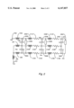
- FIG. 2 is a schematic diagram showing an example of the proposed bypass capacitor-power bus architecture represented in FIG. 1.
- Terminal 200 represents the point at which Vdd is applied to the package pin and terminal 201 represents the point at which Vss is applied to the package pin.
- Inductor 204 represents the package lead and bond wire inductance in bringing Vdd from the package pin to the internal chip Vdd bus.
- Inductor 202 represents package lead inductance in bringing Vss form the package pin to the package's bonding pad.
- the top most metal level which is the capacitor plate is wire bonded to the Vss pad of the package along with the chip's Vss.
- Symbols 208A, 208B, and 208C represent the load presented to the power supply by chip's circuitry.
- Inductor 203 represents the bond wire inductance in going from the Vss bond pad on the package to the Vss bond pad of the chip and inductor 207 represents the inductance in going form the Vss bond pad on the package to the bond pad of the top level metal 100 or top capacitor plate of the chip.
- Capacitors 205A, 205B and 205C are a lumped element representation of the distributed capacitance existing between the top metal capacitor plate 100 and the Vdd bus 102 and capacitors 206A, 206B, and 206C are a lumped element representation of the distributed capacitance between the top metal capacitor plate 100 and the Vss bus 103.
- Inductors 209A and 209B and resistors 211A and 211B are the lumped element representation of the distributed inductance and resistance of the chip's main Vdd bus 102.
- Inductors 213A and 213B and resistors 214A and 214B are the lumped element representation of the distributed inductance and resistance of the chip's main Vss bus 103.
- inductors 210 and resistors 212A and 212B are the lumped element representation of the distributed inductance and resistance of the chip's top metal capacitor plate 100. Note that for the Vdd node 215 and Vss node 216 remote from the bonding pads that there is local capacitive coupling between these power supply nodes via capacitors 205C and 206C. Thus, the effects of the parasitic inductances including various inductances such as that due to bond wires, package leads, and chip wiring and the effects of parasitic bus resistance is mitigated by the distributed capacitance of the invention while only costing one masking step. It should be noted that the reason for bonding out the top metal capacitor plate is to prevent it from floating and thereby charging via electrostatic induction.
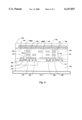
- FIG. 3 shows a top down view of the proposed capacitor structure.
- the top capacitor plate 306 covers the underlying Vdd 308 and Vss 307 buses. Three different methods of bonding the top plate to a power terminal are illustrated. In the example shown the top capacitor plate is tied to Vss although it could have been tied instead to Vdd.
- the capacitor plate 306 ties to a Vss package pad 305 via a bond wire 304 and a pad 301 which is directly connected to the top capacitor plate 306.
- Another bond wire 303 is shown which connects a chip Vss pad 300 to the shared package Vss pad 305. It is also possible that the top capacitor plate 306 does not have to share a package Vss pad with a Vss chip pad if there is a sufficient number of pads available.
- a bond wire 315 is run from a package Vss pad 316 to a chip Vss pad 314.
- a bond wire 313 connecting to a capacitor plate pad 312.
- the capacitor plate pad is made by using a pad mask opening 312.
- Vss metal 307 is under the capacitor plate pad 312. This is done so that if the thin capacitor dielectric material 101 fails due to the bonding pressure there would exist a harmless short from the capacitor plate to Vss.
- a bond wire 310 connects a capacitor plate pad 309 to the package floor metal plate 311. This scheme assumes that the package floor metal is attached to Vss which is typical for the common P substrate CMOS process.
- holes or openings can be etched into the capacitor plate 306 if some part of the upper metal interconnect layer is used for signal routing as well as for Vss 307 and Vdd 308.
- This layer for signal interconnect is feasable provided most of this layer is used for power bus routing so that a significant amount of power bus bypass capacitance can be created using the capacitor plate layer 306.
- multiple independent power busses can make use of the capacitor plate by patterning the plate layer into several separate plates with separate pad connections which correspond to the particular power bus set being bypassed.
- FIG. 4 shows an alternate version of the bypass capacitor.
- another masking layer has been added to form contacts 400A and 400B between the upper capacitor plate 100 and, in the case shown, the Vdd main bus line 102. It is acknowledged that this connection could have been made to Vss instead of Vdd.
- the advantage in adding the contacts 400 is the elimination of the wire bond(s) and the increase in local capacitance since local electrostatic coupling from Vdd to Vss is done through one dielectric thickness instead of two.
- Both the one and two mask versions of the "on" chip power supply capacitor of the invention can be implemented as an option. That is, the given chip can be made either with or without the bypass capacitor. If it is determined that the power bus bypass capacitor is not needed then the masking steps associated with the capacitor can be eliminated for the sake of cost. The determination of whether to include the capacitor in production can be made by making wafer splits with and without the capacitor layer. Performance comparisons can then be made which include speed, yield, ESD tolerance, etc.
- the top most metal level 100 acts as a capacitor plate in the Charge Device Model (CDM) test.
- CDM chip coupling will be to Vss for any charged external metal object at the bottom of the package because of the package's substrate tie plate 115 or to the capacitor plate metal 100 for any charged metal object at the top of the package.
- FIG. 5 is a schematic diagram of a pad protected by an N+/substrate diode Ddd 500 whose anode is connected to Vss and by a P+ well diode Ddd 501 whose cathode is connected to Vdd.
- Inverter 502 is being protected by the diodes during an ESD event.
- Cps 503 represents the aforementioned Vdd to Vss bypass capacitor and other Vdd to Vss capacitances such as well to substrate junction capacitance. For the sake of this discussion, Cps is shown without parasitics. Also shown is a CDM capacitor (Ccdm) 504 and its discharge impedance element 505.
- Ccdm 504 is formed by placing a packaged chip on a metal plate which capacitively couples to the die surface through the chip package material.
- the capacitance Ccdm 504 is determined by the die area, the thickness of the package material, and the dielectric constant of the package material.
- the discharge impedance 505 is determine by the arc resistance, electromagnetic radiation, and parasitic inductances such as lead and bond wire inductance.
- Ccdm is typically a few pico Farads (pFs).
- the CDM discharge is made with a probe 506 which is grounded to the plate.
- the probe 506 is brought into contact with a package pin of a die which has been charged slowly to some potential.
- Cdcm 504 then rapidly discharges into the package pin.
- Dss 500 conducts.
- Ddd 501 conducts and charges Cps 503.
- the operating voltage of integrated circuits are expected to be as low as 1.0V with gate oxide thicknesses of about 30A.
- the thin gate dielectric means that the voltages inside the chip must clamped to only a few volts during an ESD transient. In CDM the peak current can be several amps. To keep the internal voltage with a few volts thus preventing a catastrophic oxide rupture the impedance of the chip components, i.e. the pad diodes 500 and 501 and bus coupling capacitance must be low.
- the diode "on" resistance can be designed to be a couple of tenths of an ohm so that less than 2 volts will be dropped across it for a 5 amp CDM discharge.
- the voltage dropped across Cps during a positive voltage CDM discharge can be very small depending on the size of Cps 503 relative to Ccdm 504.
- a Cps to Ccdm ratio of several thousand can be achieved which attenuates the CDM discharge voltage by that amount if parasitics are ignored.
- HBM Human Body Model discharges are also favorably impacted by a large on chip power supply bypass capacitor.
- a 100 pF capacitor is used as the stress source with a source resistance of 1.5 K ⁇ .
- the attenuation factor for an HBM discharge is on the order of several hundred to one.
Abstract
An integrated circuit includes main power busses located on the next to the top most level of metal and a top level of metal separated from the main power busses by a thin dielectric. The top most level metal is connected to one of the power buses either through bond wires or through contacts. This structure provides a distributed bypass capacitance between the power buses thus stabilizing the power bus voltage within the integrated circuit. Furthermore, this capacitance structure can be optional and can be made with one or two masking steps.
Description
1. Field of the Invention.
This invention relates to the field of semiconductor integrated circuits, and particularly to an improvement in constructing an on chip power supply bypass capacitor to suppress transient voltage spikes.
2. Description of the Related Art
Capacitance bypassing of an integrated circuit's power supply nodes is typically done in moderate to high speed applications in order to filter out transient voltage spikes which are a consequence of transient current flow due to logic switching. With larger die sizes and smaller geometry transistors current transients on integrated circuits have been increasing in magnitude as the technology evolves. Even the small inductance of package leads, bond wires, and chip interconnect wires causes an unacceptable amount of voltage spiking or bouncing which has a disruptive effect on logic and analog integrated circuits.
Capacitors can be placed on a printed circuit board near the integrated circuit's power pins, Vss and Vdd, but the transient suppression is limited by lead and bond wire inductance. Capacitors can also be placed in a package along side the chip die but bond wire inductance limits performance. U.S. Pat. No. 5,629,240 a means is described of attaching a power supply bypass capacitor directly on to a chip in order to reduce parasitic inductance.
The most ideal capacitor associated with chip power bus bypassing is one which distributes the capacitance over the chip's power supply lines or wires and, correspondingly, offers very little parasitic inductance. With a large distributed "on` chip capacitor it is possible to reduce the number of power pins since multiple power pins for a given power bus are largely a consequence of the need to reduce package pin and bond wire inductance. Another desirable quality of a large distributed power bus bypass capacitor is to improve Electrostatic Discharge (ESD) protection when pad diode clamps to ground and power are used.
There are patents that describe "on" chip means to build ground to power bus capacitors including MOS capacitors and metal-insulator-metal capacitors. U.S. Pat. No. 4,937,649 a metal-insulator-metal capacitor is described in which one level of metal is used for both ground routing and as a bypass capacitor plate and a second level of metal is used for power routing and as the second bypass capacitor plate. The disadvantage of this scheme is that it requires more than two additional masking steps in order to create the two metal levels and the metal connections to the lower levels of metal in a multi-metal integrated circuit.
According to the present invention, there is provided a semiconductor integrated circuit comprising a semiconductor substrate, at least two power supply buses which provide power to logic gate, memory cells, analog circuits, etc., and a capacitor distributed between the power supply buses. One side of the capacitor has a large plate which is electrostaticly coupled to a plurality of plates connected to the ground and power pins. The plurality of ground and power plates also act as normal power distribution wires for underlying circuitry. Furthermore, the large capacitor plate is connected via one or more bond wires to either ground or to a power rail. Alternately, the large capacitor plate can be connected to one of the power rails by adding a contact step which requires adding a masking step. Between the large capacitor plate and the plurality of ground and power plates there is a deposited dielectric material. The capacitor structure requires the application of only one mask to fabricate. In addition, the circuit can be laid out so as to use the capacitor layer as a option. That is, this "on" chip power bus bypass capacitor can either be applied or omitted without affecting the layout of the integrated circuit unlike other approaches. Thus, if it is determined that a given chip does not require the capacitor layer then this layer and its associated masking step and processing steps can be omitted in the interest of reducing cost. On the other hand, this layer can be applied if it is determined that a high degree of power bus capacitive bypassing is required.
In accordance with the present invention, since the capacitor is distributively connected between the ground and power supply wires or rails, the transient voltage spikes are significantly attenuated throughout the circuitry of the integrated circuit. Furthermore, chip pin tolerance to Electro-Static Discharge (ESD) is improved by the capacitor providing a power to ground current shunt path.
U.S. Pat. No. 4,937,649. This patent describes a power bus capacitor formed with two layers of metal where one is ground or Vss and the other is Vdd. The capacitor plates are also use as major buses.
U.S. Pat. No. 4,737,830. This patent describes how to build a Vcc to Vss power bus capacitor using a thin, thermally grown oxide over a semiconductor.
U.S. Pat. No. 5,587,333. This patent describes how to build an "on" chip power supply bypass capacitor using a MOS capacitor.
U.S. Pat. No. 5,482,897. This patent describes how a chip ground plane is created by depositing and patterning metal on top of the chip.
FIG. 1 shows a cross section diagram of the proposed "on" chip bypass capacitor including details of structures found in a standard CMOS process.
FIG. 2 is a schematic diagram of an example of the proposed bypass capacitor-power bus architecture represented in FIG. 1.
FIG. 3 shows three different methods of bonding the top capacitor plate to a power rail which in this example is Vss.
FIG. 4 shows an alternate version of the bypass capacitor in which contacts are used to connect the top capacitor plate to a power rail rather than using bonding wires.
FIG. 5 shows an equivalent circuit diagram associated with the Charge Device Model used in ESD testing interacting with the power bus capacitor.
With the introduction of Chemical Mechanical Polishing (CMP) multiple levels of metal are available in the manufacture of integrated circuit. A common practice for a process with several levels of interconnect metal is to reserve the top most layer for major power bus routing.
FIG. 1 shows a cross section diagram of the proposed "on" chip bypass capacitor. The cross section includes structural features normally associated with a standard P substrate, locos isolated, CMOS process. In this example there are 4 levels of CMP metal which are used for interconnect and a 5th or top layer metal 100 which is used as a capacitor plate. The main power 102 and ground 103 distribution rails or Vdd and Vss, respectively, are routed exclusively in the 4th level of metal. The 4th level metal functions as a plurality of capacitor plates separated from the top capacitor plate 100 by a thin dielectric. The thin capacitor dielectric can be realized using such readily available process materials such as, but not limited to, silicon nitride, deposited oxide, Oxide-Nitride-Oxide (ONO), etc. The top capacitor plate 100 is connected to either Vss or Vdd via a bond wire. Note that a pad opening 119 is made in the overcoat protective layer 120 so that the bond wire 105 can be attached to the top capacitor plate 100. If it is connected to Vss a capacitor is formed between the Vdd rails 102 and the top capacitor plate 100. Conversely, if the top capacitor plate 100 is connected to Vdd then a capacitor is formed between the Vss rails 103 and the top capacitor plate 100.
Interlevel connecting stack 121 connects the main Vdd bus 102 to the local Vdd bus 116 and interlevel connecting stack 115 connects main Vss 103 to the local Vss bus 118. The interlevel connecting stacks 121 and 115 are comprised of tungsten plugs 117 and other metal layers 114 which, in the case shown in FIG. 1, are levels 2 and 3. Also shown in FIG. 1 are the thick inter level dielectric 122, field oxide associated with a locos process 104, the gate 113 of a PFET, the P+ source 110 of a PFET which is connected to the local Vdd 116, the N+ well of a PFET 107, the N+ well tie 106 which connects to the local Vdd bus 116, the drain of the PFET 124, a P+ substrate tie 108 which is connected to the local Vss 118, an N+ source 109 of an NFET, the gate 112 of an NFET, the drain 111 of the NFET, and examples of inter level metal signal interconnect 114 on metal levels 2 and 3. The silicon substrate 123 is attached to the die plate or floor 115 of the chips encapsulating package which is connected to Vss via the lead frame. The protective overcoat insulating layer 120 is shown on top of the capacitor plate metal 100.
The cross section of FIG. 1 is for illustration purposes. It is acknowledged that the capacitor forming techniques defined here can be applied to processes with any number of metal layers, to any isolation scheme such as shallow trench isolation, and, in general, to any type of semiconductor process including bipolar, GaAs, SOI, etc.
To make the capacitor according to this invention the following steps are taken. The starting point for this discussion is after metal layer 102/103 has been deposited and patterned. It is assumed the metal level comprising 102 and 103 is the last normal level of metal required to realize a given integrated circuit without a metal to metal internal capacitor and that the main Vdd and Vss lines are routed on this level. A thin dielectric 101 is then deposited over the Vdd/Vss conductors, 102 and 103, respectively. Next, metal 100 is deposited over the thin dielectric and patterned with a mask. The capacitor metal layer 100 includes a pad layout where a pad mask opening 119 has been applied. A bond wire 105 is connected from the pad from a bonding pad 126 associated with the capacitor plate 100 to either Vss or Vdd of the package or to a Vss/Vdd pad on the last normal metal or to the pad floor. It is acknowledged that more than one pad connection to the capacitor metal plate 100 can be made depending on capacitor performance and available space.
To provide for good metal step coverage of the top capacitor plate 100 over the Vdd 102 and Vss 103 busses one of two steps can be taken. One to form a spacer 125 at the edge of the Vdd 102 and Vss metal lines. The spacer is formed by depositing a thick insulating film such as, but not limited to, oxide or nitride. The insulator is then selectively etched such that the insulator is no longer on top of the Vdd 102 or Vss 103 metal. Due to the differential thickness of the deposited film on topography, there will be residual insulator material clinging to the edges of the Vdd 102 and Vss 103 metal. The spacer thus formed will provide a more gradual slope for the top plate capacitor 100 metal. Another method is to perform a sloped etch on the metal layer used to form Vdd 102 and Vss 103. A positive slope 127 on the edges of this metal layer will provide better step coverage for the top capacitor plate.
FIG. 2 is a schematic diagram showing an example of the proposed bypass capacitor-power bus architecture represented in FIG. 1. Terminal 200 represents the point at which Vdd is applied to the package pin and terminal 201 represents the point at which Vss is applied to the package pin. Inductor 204 represents the package lead and bond wire inductance in bringing Vdd from the package pin to the internal chip Vdd bus. Inductor 202 represents package lead inductance in bringing Vss form the package pin to the package's bonding pad. In this example it is assumed that the top most metal level which is the capacitor plate is wire bonded to the Vss pad of the package along with the chip's Vss. Symbols 208A, 208B, and 208C represent the load presented to the power supply by chip's circuitry. Inductor 203 represents the bond wire inductance in going from the Vss bond pad on the package to the Vss bond pad of the chip and inductor 207 represents the inductance in going form the Vss bond pad on the package to the bond pad of the top level metal 100 or top capacitor plate of the chip. Capacitors 205A, 205B and 205C are a lumped element representation of the distributed capacitance existing between the top metal capacitor plate 100 and the Vdd bus 102 and capacitors 206A, 206B, and 206C are a lumped element representation of the distributed capacitance between the top metal capacitor plate 100 and the Vss bus 103. Inductors 209A and 209B and resistors 211A and 211B are the lumped element representation of the distributed inductance and resistance of the chip's main Vdd bus 102. Inductors 213A and 213B and resistors 214A and 214B are the lumped element representation of the distributed inductance and resistance of the chip's main Vss bus 103. Finally, inductors 210 and resistors 212A and 212B are the lumped element representation of the distributed inductance and resistance of the chip's top metal capacitor plate 100. Note that for the Vdd node 215 and Vss node 216 remote from the bonding pads that there is local capacitive coupling between these power supply nodes via capacitors 205C and 206C. Thus, the effects of the parasitic inductances including various inductances such as that due to bond wires, package leads, and chip wiring and the effects of parasitic bus resistance is mitigated by the distributed capacitance of the invention while only costing one masking step. It should be noted that the reason for bonding out the top metal capacitor plate is to prevent it from floating and thereby charging via electrostatic induction.
FIG. 3 shows a top down view of the proposed capacitor structure. The top capacitor plate 306 covers the underlying Vdd 308 and Vss 307 buses. Three different methods of bonding the top plate to a power terminal are illustrated. In the example shown the top capacitor plate is tied to Vss although it could have been tied instead to Vdd.
At the top of the diagram the capacitor plate 306 ties to a Vss package pad 305 via a bond wire 304 and a pad 301 which is directly connected to the top capacitor plate 306. Another bond wire 303 is shown which connects a chip Vss pad 300 to the shared package Vss pad 305. It is also possible that the top capacitor plate 306 does not have to share a package Vss pad with a Vss chip pad if there is a sufficient number of pads available.
On the right hand side of the diagram another method of bonding is illustrated. In this case a bond wire 315 is run from a package Vss pad 316 to a chip Vss pad 314. On the same pad 314 which has two bonding sites there is a bond wire 313 connecting to a capacitor plate pad 312. The capacitor plate pad is made by using a pad mask opening 312. Note that Vss metal 307 is under the capacitor plate pad 312. This is done so that if the thin capacitor dielectric material 101 fails due to the bonding pressure there would exist a harmless short from the capacitor plate to Vss.
Finally, on the bottom of the diagram a bond wire 310 connects a capacitor plate pad 309 to the package floor metal plate 311. This scheme assumes that the package floor metal is attached to Vss which is typical for the common P substrate CMOS process.
It should be noted that holes or openings can be etched into the capacitor plate 306 if some part of the upper metal interconnect layer is used for signal routing as well as for Vss 307 and Vdd 308. Using this layer for signal interconnect is feasable provided most of this layer is used for power bus routing so that a significant amount of power bus bypass capacitance can be created using the capacitor plate layer 306. Also, multiple independent power busses can make use of the capacitor plate by patterning the plate layer into several separate plates with separate pad connections which correspond to the particular power bus set being bypassed.
FIG. 4 shows an alternate version of the bypass capacitor. In this case another masking layer has been added to form contacts 400A and 400B between the upper capacitor plate 100 and, in the case shown, the Vdd main bus line 102. It is acknowledged that this connection could have been made to Vss instead of Vdd. The advantage in adding the contacts 400 is the elimination of the wire bond(s) and the increase in local capacitance since local electrostatic coupling from Vdd to Vss is done through one dielectric thickness instead of two.
Both the one and two mask versions of the "on" chip power supply capacitor of the invention can be implemented as an option. That is, the given chip can be made either with or without the bypass capacitor. If it is determined that the power bus bypass capacitor is not needed then the masking steps associated with the capacitor can be eliminated for the sake of cost. The determination of whether to include the capacitor in production can be made by making wafer splits with and without the capacitor layer. Performance comparisons can then be made which include speed, yield, ESD tolerance, etc.
A desirable quality of having a large, "on" chip capacitor is improved ESD protection. The top most metal level 100 acts as a capacitor plate in the Charge Device Model (CDM) test. In FIG. 1 the CDM chip coupling will be to Vss for any charged external metal object at the bottom of the package because of the package's substrate tie plate 115 or to the capacitor plate metal 100 for any charged metal object at the top of the package.
FIG. 5 is a schematic diagram of a pad protected by an N+/substrate diode Ddd 500 whose anode is connected to Vss and by a P+ well diode Ddd 501 whose cathode is connected to Vdd. Inverter 502 is being protected by the diodes during an ESD event. Cps 503 represents the aforementioned Vdd to Vss bypass capacitor and other Vdd to Vss capacitances such as well to substrate junction capacitance. For the sake of this discussion, Cps is shown without parasitics. Also shown is a CDM capacitor (Ccdm) 504 and its discharge impedance element 505. For test purposes, Ccdm 504 is formed by placing a packaged chip on a metal plate which capacitively couples to the die surface through the chip package material. The capacitance Ccdm 504 is determined by the die area, the thickness of the package material, and the dielectric constant of the package material. The discharge impedance 505 is determine by the arc resistance, electromagnetic radiation, and parasitic inductances such as lead and bond wire inductance. Ccdm is typically a few pico Farads (pFs).
The CDM discharge is made with a probe 506 which is grounded to the plate. The probe 506 is brought into contact with a package pin of a die which has been charged slowly to some potential. Cdcm 504 then rapidly discharges into the package pin. For a positive CDM voltage on the external plate Dss 500 conducts. For a negative CDM voltage on the external plate Ddd 501 conducts and charges Cps 503.
For future processes the operating voltage of integrated circuits are expected to be as low as 1.0V with gate oxide thicknesses of about 30A. The thin gate dielectric means that the voltages inside the chip must clamped to only a few volts during an ESD transient. In CDM the peak current can be several amps. To keep the internal voltage with a few volts thus preventing a catastrophic oxide rupture the impedance of the chip components, i.e. the pad diodes 500 and 501 and bus coupling capacitance must be low. The diode "on" resistance can be designed to be a couple of tenths of an ohm so that less than 2 volts will be dropped across it for a 5 amp CDM discharge. The voltage dropped across Cps during a positive voltage CDM discharge can be very small depending on the size of Cps 503 relative to Ccdm 504. For reasonable dielectric thicknesses of the bus bypass capacitor, a Cps to Ccdm ratio of several thousand can be achieved which attenuates the CDM discharge voltage by that amount if parasitics are ignored.
Human Body Model discharges are also favorably impacted by a large on chip power supply bypass capacitor. In the HBM a 100 pF capacitor is used as the stress source with a source resistance of 1.5 KΩ. Thus, the attenuation factor for an HBM discharge is on the order of several hundred to one.
Claims (3)
1. A semiconductor integrated circuit comprising:
a semiconductor substrate;
circuits formed on said substrate;
power rails and ground rails formed on said substrate, each of said rails being used to supply power for said circuits and said rails being formed on a top most interconnect metal layer of said circuits;
an insulating layer formed on said substrate over said power and ground rails;
a metal layer formed on said insulating layer acting as a top capacitor plate with said power and ground rails acting as a lower capacitor plate and said metal layer substantially covering said rails thereby forming a power supply bypass capacitor;
means for connecting said top capacitor plate to at least one of said power rails or to at least one of said ground rails;
said means for connecting said top capacitor plate to at least one of said power rails or to at least one of said ground rails comprising a bond wire leading from a bond pad connected to said top capacitor plate to a bond pad connected to at least one of said power rails or to at least one of said ground rails.
2. A semiconductor integrated circuit comprising:
a semiconductor substrate;
circuits formed on said substrate;
power rails and ground rails formed on said substrate, each of said rails being used to supply power for said circuits and said rails being formed on a top most interconnect metal layer of said circuits;
an insulating layer formed on said substrate over said power and ground rails;
a metal layer formed on said insulating layer acting as a top capacitor plate with said power and ground rails acting as a lower capacitor plate and said metal layer substantially covering said rails thereby forming a power supply bypass capacitor;
means for connecting said top capacitor plate to at least one of said power rails or to at least one of said ground rails;
said means for connecting said top capacitor plate to at least one of said power rails or to at least one of said ground rails comprising a bond wire leading from a bond pad connected to said top capacitor plate to a bond pad located on a package which connects to a power pin or to a ground pin.
3. A semiconductor integrated circuit comprising:
a semiconductor substrate connected to a package floor metal plate;
circuits formed on said substrate;
power rails and ground rails formed on said substrate, each of said rails being used to supply power for said circuits and said rails being formed on a top most interconnect metal layer of said circuits;
an insulating layer formed on said substrate over said power and ground rails;
a metal layer formed on said insulating layer acting as a top capacitor plate with said power and ground rails acting as a lower capacitor plate and said metal layer substantially covering said rails thereby forming a power supply bypass capacitor;
means for connecting said top capacitor plate to at least one of said power rails or to at least one of said ground rails;
said means for connecting said top capacitor plate to at least one of said power rails or to at least one of said ground rails comprising a bond wire leading from a bond pad connected to said top capacitor plate to said package floor metal plate.
Priority Applications (1)
| Application Number | Priority Date | Filing Date | Title |
|---|---|---|---|
| US08/946,555 US6147857A (en) | 1997-10-07 | 1997-10-07 | Optional on chip power supply bypass capacitor |
Applications Claiming Priority (1)
| Application Number | Priority Date | Filing Date | Title |
|---|---|---|---|
| US08/946,555 US6147857A (en) | 1997-10-07 | 1997-10-07 | Optional on chip power supply bypass capacitor |
Publications (1)
| Publication Number | Publication Date |
|---|---|
| US6147857A true US6147857A (en) | 2000-11-14 |
Family
ID=25484649
Family Applications (1)
| Application Number | Title | Priority Date | Filing Date |
|---|---|---|---|
| US08/946,555 Expired - Fee Related US6147857A (en) | 1997-10-07 | 1997-10-07 | Optional on chip power supply bypass capacitor |
Country Status (1)
| Country | Link |
|---|---|
| US (1) | US6147857A (en) |
Cited By (37)
| Publication number | Priority date | Publication date | Assignee | Title |
|---|---|---|---|---|
| US20020055246A1 (en) * | 2000-08-30 | 2002-05-09 | Tongbi Jiang | Method and apparatus for reducing substrate bias voltage drop |
| US6558998B2 (en) * | 1998-06-15 | 2003-05-06 | Marc Belleville | SOI type integrated circuit with a decoupling capacity and process for embodiment of such a circuit |
| US6591406B2 (en) * | 1999-12-27 | 2003-07-08 | Nec Electronics Corporation | Semiconductor apparatus including bypass capacitor having structure for making automatic design easy, and semiconductor apparatus layout method |
| US6608363B1 (en) * | 2001-03-01 | 2003-08-19 | Skyworks Solutions, Inc. | Transformer comprising stacked inductors |
| US20030200509A1 (en) * | 2002-04-23 | 2003-10-23 | Yasutaka Takabayashi | Semiconductor IC with an inside capacitor for a power supply circuit and a method of automatically designing the same |
| US6695214B1 (en) * | 1998-02-04 | 2004-02-24 | Schlumberger, Systémes | Device with integrated circuit made secure by attenuation of electric signatures |
| US20040150026A1 (en) * | 2003-02-05 | 2004-08-05 | Sun Microsystems, Inc. | Metal insulator metal capacitor |
| US6777772B1 (en) * | 1998-05-22 | 2004-08-17 | Renesas Technology Corp. | Semiconductor device having improved trench structure |
| US20040188841A1 (en) * | 2003-03-26 | 2004-09-30 | Taiwan Semiconductor Manufacturing Co., Ltd. | Extended length metal line for improved ESD performance |
| US20040212040A1 (en) * | 2003-04-23 | 2004-10-28 | Kabushiki Kaisha Toshiba | Semiconductor integrated circuit device and method of manufacturing the same |
| US20050008732A1 (en) * | 2003-07-11 | 2005-01-13 | Petros Gebreselassie | Chewing gum and confectionery compositions containing a stain removing complex, and methods of making and using the same |
| US20050012159A1 (en) * | 2003-07-18 | 2005-01-20 | Yasuhiko Sekimoto | Semiconductor device with bypass capacitor |
| US20050051897A1 (en) * | 2003-09-05 | 2005-03-10 | Via Technologies, Inc. | Bonding pad design for impedance matching improvement |
| US20050194643A1 (en) * | 2002-12-20 | 2005-09-08 | Williams Richard K. | Testable electrostatic discharge protection circuits |
| US20050242438A1 (en) * | 2002-05-07 | 2005-11-03 | Andrea Cathelin | Circuit comprising a capacitor and at least one semiconductor component, and method of designing same |
| US20060138635A1 (en) * | 2004-05-17 | 2006-06-29 | Mitsubishi Denki Kabushiki Kaisha | Power semiconductor device |
| US7087927B1 (en) * | 2003-07-22 | 2006-08-08 | National Semiconductor Corporation | Semiconductor die with an editing structure |
| US20070013290A1 (en) * | 2005-07-15 | 2007-01-18 | Silicon Integrated Systems Corp. | Closed ring structure of electrostatic discharge circuitry |
| US20070182521A1 (en) * | 2003-05-27 | 2007-08-09 | Megica Corporation | High performance system-on-chip inductor using post passivation process |
| US20080001302A1 (en) * | 2000-10-18 | 2008-01-03 | Megica Corporation | Post passivation interconnection schemes on top of IC chip |
| US20080035972A1 (en) * | 1998-12-21 | 2008-02-14 | Megica Corporation | High performance system-on-chip using post passivation process |
| US20080045003A1 (en) * | 2002-10-15 | 2008-02-21 | Megica Corporation | Method of wire bonding over active area of a semiconductor circuit |
| US20090230446A1 (en) * | 2008-03-17 | 2009-09-17 | Technology Alliance Group, Inc. | Semiconductor device and bypass capacitor module |
| USRE41355E1 (en) * | 1999-03-17 | 2010-05-25 | Intel Corporation | Method for placing active circuits beneath active bonding pads |
| US7863654B2 (en) | 1998-12-21 | 2011-01-04 | Megica Corporation | Top layers of metal for high performance IC's |
| US7960269B2 (en) | 2005-07-22 | 2011-06-14 | Megica Corporation | Method for forming a double embossing structure |
| US7973629B2 (en) | 2001-09-04 | 2011-07-05 | Megica Corporation | Method for making high-performance RF integrated circuits |
| US8008775B2 (en) | 2004-09-09 | 2011-08-30 | Megica Corporation | Post passivation interconnection structures |
| US8018060B2 (en) | 2004-09-09 | 2011-09-13 | Megica Corporation | Post passivation interconnection process and structures |
| US8178435B2 (en) | 1998-12-21 | 2012-05-15 | Megica Corporation | High performance system-on-chip inductor using post passivation process |
| US8384189B2 (en) | 2005-03-29 | 2013-02-26 | Megica Corporation | High performance system-on-chip using post passivation process |
| US8421158B2 (en) | 1998-12-21 | 2013-04-16 | Megica Corporation | Chip structure with a passive device and method for forming the same |
| US8618607B1 (en) * | 2012-07-02 | 2013-12-31 | Globalfoundries Inc. | Semiconductor devices formed on a continuous active region with an isolating conductive structure positioned between such semiconductor devices, and methods of making same |
| US9070684B2 (en) | 2012-04-30 | 2015-06-30 | Avago Technologies General Ip (Singapore) Pte. Ltd. | Integrated circuit power grid with improved routing resources and bypass capacitance |
| US10262938B2 (en) * | 2017-08-31 | 2019-04-16 | Vanguard International Semiconductor Corporation | Semiconductor structure having conductive layer overlapping field oxide |
| US10692808B2 (en) | 2017-09-18 | 2020-06-23 | Qualcomm Incorporated | High performance cell design in a technology with high density metal routing |
| US10734279B2 (en) * | 2017-05-09 | 2020-08-04 | Taiwan Semiconductor Manufacturing Company Ltd. | Semiconductor package device with integrated antenna and manufacturing method thereof |
Citations (14)
| Publication number | Priority date | Publication date | Assignee | Title |
|---|---|---|---|---|
| US4598307A (en) * | 1982-09-22 | 1986-07-01 | Fujitsu Limited | Integrated circuit device having package with bypass capacitor |
| US4737830A (en) * | 1986-01-08 | 1988-04-12 | Advanced Micro Devices, Inc. | Integrated circuit structure having compensating means for self-inductance effects |
| US4864464A (en) * | 1989-01-09 | 1989-09-05 | Micron Technology, Inc. | Low-profile, folded-plate dram-cell capacitor fabricated with two mask steps |
| US4929989A (en) * | 1988-05-10 | 1990-05-29 | Nec Corporation | MOS type semiconductor device potential stabilizing circuit with series MOS capacitors |
| US4937649A (en) * | 1986-09-12 | 1990-06-26 | Nec Corporation | Semiconductor integrated circuit having a capacitor for stabilizing a voltage at a power supplying wiring |
| JPH02260559A (en) * | 1989-03-31 | 1990-10-23 | Seiko Epson Corp | Semiconductor integrated circuit device |
| US5200364A (en) * | 1990-01-26 | 1993-04-06 | Texas Instruments Incorporated | Packaged integrated circuit with encapsulated electronic devices |
| US5482897A (en) * | 1994-07-19 | 1996-01-09 | Lsi Logic Corporation | Integrated circuit with on-chip ground plane |
| US5590017A (en) * | 1995-04-03 | 1996-12-31 | Aluminum Company Of America | Alumina multilayer wiring substrate provided with high dielectric material layer |
| US5598029A (en) * | 1993-09-13 | 1997-01-28 | Nec Corporation | Power supply wiring for semiconductor device |
| US5629240A (en) * | 1994-12-09 | 1997-05-13 | Sun Microsystems, Inc. | Method for direct attachment of an on-chip bypass capacitor in an integrated circuit |
| US5652693A (en) * | 1993-11-12 | 1997-07-29 | Fujitsu Limited | Substrate with thin film capacitor and insulating plug |
| US5730835A (en) * | 1996-01-31 | 1998-03-24 | Micron Technology, Inc. | Facet etch for improved step coverage of integrated circuit contacts |
| US5834348A (en) * | 1993-01-27 | 1998-11-10 | Samsung Electronics Co., Ltd. | Method for manufacturing a semiconductor device having a ferroelectric capacitor |
-
1997
- 1997-10-07 US US08/946,555 patent/US6147857A/en not_active Expired - Fee Related
Patent Citations (15)
| Publication number | Priority date | Publication date | Assignee | Title |
|---|---|---|---|---|
| US4598307A (en) * | 1982-09-22 | 1986-07-01 | Fujitsu Limited | Integrated circuit device having package with bypass capacitor |
| US4737830A (en) * | 1986-01-08 | 1988-04-12 | Advanced Micro Devices, Inc. | Integrated circuit structure having compensating means for self-inductance effects |
| US4937649A (en) * | 1986-09-12 | 1990-06-26 | Nec Corporation | Semiconductor integrated circuit having a capacitor for stabilizing a voltage at a power supplying wiring |
| US4929989A (en) * | 1988-05-10 | 1990-05-29 | Nec Corporation | MOS type semiconductor device potential stabilizing circuit with series MOS capacitors |
| US4864464A (en) * | 1989-01-09 | 1989-09-05 | Micron Technology, Inc. | Low-profile, folded-plate dram-cell capacitor fabricated with two mask steps |
| JPH02260559A (en) * | 1989-03-31 | 1990-10-23 | Seiko Epson Corp | Semiconductor integrated circuit device |
| US5200364A (en) * | 1990-01-26 | 1993-04-06 | Texas Instruments Incorporated | Packaged integrated circuit with encapsulated electronic devices |
| US5834348A (en) * | 1993-01-27 | 1998-11-10 | Samsung Electronics Co., Ltd. | Method for manufacturing a semiconductor device having a ferroelectric capacitor |
| US5598029A (en) * | 1993-09-13 | 1997-01-28 | Nec Corporation | Power supply wiring for semiconductor device |
| US5652693A (en) * | 1993-11-12 | 1997-07-29 | Fujitsu Limited | Substrate with thin film capacitor and insulating plug |
| US5482897A (en) * | 1994-07-19 | 1996-01-09 | Lsi Logic Corporation | Integrated circuit with on-chip ground plane |
| US5629240A (en) * | 1994-12-09 | 1997-05-13 | Sun Microsystems, Inc. | Method for direct attachment of an on-chip bypass capacitor in an integrated circuit |
| US5780930A (en) * | 1994-12-09 | 1998-07-14 | Sun Microsystems, Inc. | Method for direct attachment of an on-chip bypass capacitor in an integrated circuit |
| US5590017A (en) * | 1995-04-03 | 1996-12-31 | Aluminum Company Of America | Alumina multilayer wiring substrate provided with high dielectric material layer |
| US5730835A (en) * | 1996-01-31 | 1998-03-24 | Micron Technology, Inc. | Facet etch for improved step coverage of integrated circuit contacts |
Non-Patent Citations (2)
| Title |
|---|
| Coombs, "Printed Circuits Handbook", pp. 21.19-21.20, 1996. |
| Coombs, Printed Circuits Handbook , pp. 21.19 21.20, 1996. * |
Cited By (86)
| Publication number | Priority date | Publication date | Assignee | Title |
|---|---|---|---|---|
| US6695214B1 (en) * | 1998-02-04 | 2004-02-24 | Schlumberger, Systémes | Device with integrated circuit made secure by attenuation of electric signatures |
| US6777772B1 (en) * | 1998-05-22 | 2004-08-17 | Renesas Technology Corp. | Semiconductor device having improved trench structure |
| US6558998B2 (en) * | 1998-06-15 | 2003-05-06 | Marc Belleville | SOI type integrated circuit with a decoupling capacity and process for embodiment of such a circuit |
| US20080038869A1 (en) * | 1998-12-21 | 2008-02-14 | Megica Corporation | High performance system-on-chip using post passivation process |
| US8471384B2 (en) | 1998-12-21 | 2013-06-25 | Megica Corporation | Top layers of metal for high performance IC's |
| US7884479B2 (en) | 1998-12-21 | 2011-02-08 | Megica Corporation | Top layers of metal for high performance IC's |
| US8421158B2 (en) | 1998-12-21 | 2013-04-16 | Megica Corporation | Chip structure with a passive device and method for forming the same |
| US7999384B2 (en) | 1998-12-21 | 2011-08-16 | Megica Corporation | Top layers of metal for high performance IC's |
| US8178435B2 (en) | 1998-12-21 | 2012-05-15 | Megica Corporation | High performance system-on-chip inductor using post passivation process |
| US20080042239A1 (en) * | 1998-12-21 | 2008-02-21 | Megica Corporation | High performance system-on-chip using post passivation process |
| US8415800B2 (en) | 1998-12-21 | 2013-04-09 | Megica Corporation | Top layers of metal for high performance IC's |
| US20080035972A1 (en) * | 1998-12-21 | 2008-02-14 | Megica Corporation | High performance system-on-chip using post passivation process |
| US8531038B2 (en) | 1998-12-21 | 2013-09-10 | Megica Corporation | Top layers of metal for high performance IC's |
| US8022545B2 (en) | 1998-12-21 | 2011-09-20 | Megica Corporation | Top layers of metal for high performance IC's |
| US8487400B2 (en) * | 1998-12-21 | 2013-07-16 | Megica Corporation | High performance system-on-chip using post passivation process |
| US20070181970A1 (en) * | 1998-12-21 | 2007-08-09 | Megica Corporation | High performance system-on-chip inductor using post passivation process |
| US7863654B2 (en) | 1998-12-21 | 2011-01-04 | Megica Corporation | Top layers of metal for high performance IC's |
| US8138079B2 (en) | 1998-12-21 | 2012-03-20 | Megica Corporation | Method of wire bonding over active area of a semiconductor circuit |
| USRE41355E1 (en) * | 1999-03-17 | 2010-05-25 | Intel Corporation | Method for placing active circuits beneath active bonding pads |
| US6591406B2 (en) * | 1999-12-27 | 2003-07-08 | Nec Electronics Corporation | Semiconductor apparatus including bypass capacitor having structure for making automatic design easy, and semiconductor apparatus layout method |
| US7189602B2 (en) | 2000-08-30 | 2007-03-13 | Micron Technology, Inc. | Method and apparatus for reducing substrate bias voltage drop |
| US6788552B1 (en) * | 2000-08-30 | 2004-09-07 | Micron Technology, Inc. | Method and apparatus for reducing substrate bias voltage drop |
| US20020055246A1 (en) * | 2000-08-30 | 2002-05-09 | Tongbi Jiang | Method and apparatus for reducing substrate bias voltage drop |
| US8482127B2 (en) | 2000-10-18 | 2013-07-09 | Megica Corporation | Post passivation interconnection schemes on top of IC chip |
| US7923366B2 (en) | 2000-10-18 | 2011-04-12 | Megica Corporation | Post passivation interconnection schemes on top of IC chip |
| US7919865B2 (en) | 2000-10-18 | 2011-04-05 | Megica Corporation | Post passivation interconnection schemes on top of IC chip |
| US8461686B2 (en) | 2000-10-18 | 2013-06-11 | Megica Corporation | Post passivation interconnection schemes on top of IC chip |
| US7902067B2 (en) | 2000-10-18 | 2011-03-08 | Megica Corporation | Post passivation interconnection schemes on top of the IC chips |
| US20080061444A1 (en) * | 2000-10-18 | 2008-03-13 | Megica Corporation | Post passivation interconnection schemes on top of IC chip |
| US8492900B2 (en) | 2000-10-18 | 2013-07-23 | Megica Corporation | Post passivation interconnection schemes on top of IC chip |
| US20080067694A1 (en) * | 2000-10-18 | 2008-03-20 | Megica Corporation | Post passivation interconnection schemes on top of IC chip |
| US7466007B2 (en) * | 2000-10-18 | 2008-12-16 | Megica Corporation | Post passivation interconnection schemes on top of IC chip |
| US20080001302A1 (en) * | 2000-10-18 | 2008-01-03 | Megica Corporation | Post passivation interconnection schemes on top of IC chip |
| US8004088B2 (en) | 2000-10-18 | 2011-08-23 | Megica Corporation | Post passivation interconnection schemes on top of IC chip |
| US8435883B2 (en) | 2000-10-18 | 2013-05-07 | Megica Corporation | Post passivation interconnection schemes on top of IC chips |
| US7915161B2 (en) | 2000-10-18 | 2011-03-29 | Megica Corporation | Post passivation interconnection schemes on top of IC chip |
| US7892965B2 (en) | 2000-10-18 | 2011-02-22 | Megica Corporation | Post passivation interconnection schemes on top of IC chip |
| US8188603B2 (en) | 2000-10-18 | 2012-05-29 | Megica Corporation | Post passivation interconnection schemes on top of IC chip |
| US6608363B1 (en) * | 2001-03-01 | 2003-08-19 | Skyworks Solutions, Inc. | Transformer comprising stacked inductors |
| US8384508B2 (en) | 2001-09-04 | 2013-02-26 | Megica Corporation | Method for making high-performance RF integrated circuits |
| US7973629B2 (en) | 2001-09-04 | 2011-07-05 | Megica Corporation | Method for making high-performance RF integrated circuits |
| US6732335B2 (en) * | 2002-04-23 | 2004-05-04 | Oki Electric Industry Co., Ltd. | Semiconductor IC with an inside capacitor for a power supply circuit and a method of automatically designing the same |
| US20030200509A1 (en) * | 2002-04-23 | 2003-10-23 | Yasutaka Takabayashi | Semiconductor IC with an inside capacitor for a power supply circuit and a method of automatically designing the same |
| US7282803B2 (en) * | 2002-05-07 | 2007-10-16 | Stmicroelectronics S. A. | Integrated electronic circuit comprising a capacitor and a planar interference inhibiting metallic screen |
| US20050242438A1 (en) * | 2002-05-07 | 2005-11-03 | Andrea Cathelin | Circuit comprising a capacitor and at least one semiconductor component, and method of designing same |
| US9153555B2 (en) | 2002-10-15 | 2015-10-06 | Qualcomm Incorporated | Method of wire bonding over active area of a semiconductor circuit |
| US8742580B2 (en) | 2002-10-15 | 2014-06-03 | Megit Acquisition Corp. | Method of wire bonding over active area of a semiconductor circuit |
| US8021976B2 (en) | 2002-10-15 | 2011-09-20 | Megica Corporation | Method of wire bonding over active area of a semiconductor circuit |
| US20080045003A1 (en) * | 2002-10-15 | 2008-02-21 | Megica Corporation | Method of wire bonding over active area of a semiconductor circuit |
| US8026588B2 (en) | 2002-10-15 | 2011-09-27 | Megica Corporation | Method of wire bonding over active area of a semiconductor circuit |
| US9142527B2 (en) | 2002-10-15 | 2015-09-22 | Qualcomm Incorporated | Method of wire bonding over active area of a semiconductor circuit |
| US7432555B2 (en) * | 2002-12-20 | 2008-10-07 | Advanced Analogic Technologies, Inc. | Testable electrostatic discharge protection circuits |
| US7329551B2 (en) * | 2002-12-20 | 2008-02-12 | Advanced Analogic Technologies, Inc. | Manufacturing and testing of electrostatic discharge protection circuits |
| US20050194643A1 (en) * | 2002-12-20 | 2005-09-08 | Williams Richard K. | Testable electrostatic discharge protection circuits |
| US20050202577A1 (en) * | 2002-12-20 | 2005-09-15 | Williams Richard K. | Manufacturing and testing of electrostatic discharge protection circuits |
| US7098501B2 (en) * | 2003-02-05 | 2006-08-29 | Sun Microsystems, Inc. | Thin capacitive structure |
| US20040150026A1 (en) * | 2003-02-05 | 2004-08-05 | Sun Microsystems, Inc. | Metal insulator metal capacitor |
| US20040188841A1 (en) * | 2003-03-26 | 2004-09-30 | Taiwan Semiconductor Manufacturing Co., Ltd. | Extended length metal line for improved ESD performance |
| US6888248B2 (en) * | 2003-03-26 | 2005-05-03 | Taiwan Semiconductor Manufacturing Co., Ltd | Extended length metal line for improved ESD performance |
| US20040212040A1 (en) * | 2003-04-23 | 2004-10-28 | Kabushiki Kaisha Toshiba | Semiconductor integrated circuit device and method of manufacturing the same |
| US6876059B2 (en) * | 2003-04-23 | 2005-04-05 | Kabushiki Kaisha Toshiba | Semiconductor integrated circuit device and method of manufacturing the same |
| US20070202685A1 (en) * | 2003-05-27 | 2007-08-30 | Megica Corporation | High performance system-on-chip inductor using post passivation process |
| US20070202684A1 (en) * | 2003-05-27 | 2007-08-30 | Megica Corporation | High performance system-on-chip inductor using post passivation process |
| US20070182521A1 (en) * | 2003-05-27 | 2007-08-09 | Megica Corporation | High performance system-on-chip inductor using post passivation process |
| US20050008732A1 (en) * | 2003-07-11 | 2005-01-13 | Petros Gebreselassie | Chewing gum and confectionery compositions containing a stain removing complex, and methods of making and using the same |
| US20050012159A1 (en) * | 2003-07-18 | 2005-01-20 | Yasuhiko Sekimoto | Semiconductor device with bypass capacitor |
| US7239005B2 (en) * | 2003-07-18 | 2007-07-03 | Yamaha Corporation | Semiconductor device with bypass capacitor |
| US7087927B1 (en) * | 2003-07-22 | 2006-08-08 | National Semiconductor Corporation | Semiconductor die with an editing structure |
| US7352001B1 (en) | 2003-07-22 | 2008-04-01 | National Semiconductor Corporation | Method of editing a semiconductor die |
| US6919621B2 (en) * | 2003-09-05 | 2005-07-19 | Via Technologies, Inc. | Bonding pad design for impedance matching improvement |
| US20050051897A1 (en) * | 2003-09-05 | 2005-03-10 | Via Technologies, Inc. | Bonding pad design for impedance matching improvement |
| US7368825B2 (en) * | 2004-05-17 | 2008-05-06 | Mitsubishi Denki Kabushiki Kaisha | Power semiconductor device |
| US20060138635A1 (en) * | 2004-05-17 | 2006-06-29 | Mitsubishi Denki Kabushiki Kaisha | Power semiconductor device |
| US8018060B2 (en) | 2004-09-09 | 2011-09-13 | Megica Corporation | Post passivation interconnection process and structures |
| US8008775B2 (en) | 2004-09-09 | 2011-08-30 | Megica Corporation | Post passivation interconnection structures |
| US8384189B2 (en) | 2005-03-29 | 2013-02-26 | Megica Corporation | High performance system-on-chip using post passivation process |
| US20070013290A1 (en) * | 2005-07-15 | 2007-01-18 | Silicon Integrated Systems Corp. | Closed ring structure of electrostatic discharge circuitry |
| US7960269B2 (en) | 2005-07-22 | 2011-06-14 | Megica Corporation | Method for forming a double embossing structure |
| US20090230446A1 (en) * | 2008-03-17 | 2009-09-17 | Technology Alliance Group, Inc. | Semiconductor device and bypass capacitor module |
| US8299518B2 (en) | 2008-03-17 | 2012-10-30 | Liquid Design Systems Inc. | Semiconductor device and bypass capacitor module |
| US9070684B2 (en) | 2012-04-30 | 2015-06-30 | Avago Technologies General Ip (Singapore) Pte. Ltd. | Integrated circuit power grid with improved routing resources and bypass capacitance |
| US8618607B1 (en) * | 2012-07-02 | 2013-12-31 | Globalfoundries Inc. | Semiconductor devices formed on a continuous active region with an isolating conductive structure positioned between such semiconductor devices, and methods of making same |
| US10734279B2 (en) * | 2017-05-09 | 2020-08-04 | Taiwan Semiconductor Manufacturing Company Ltd. | Semiconductor package device with integrated antenna and manufacturing method thereof |
| US11295979B2 (en) * | 2017-05-09 | 2022-04-05 | Taiwan Semiconductor Manufacturing Company Ltd. | Semiconductor package device with integrated antenna and manufacturing method thereof |
| US10262938B2 (en) * | 2017-08-31 | 2019-04-16 | Vanguard International Semiconductor Corporation | Semiconductor structure having conductive layer overlapping field oxide |
| US10692808B2 (en) | 2017-09-18 | 2020-06-23 | Qualcomm Incorporated | High performance cell design in a technology with high density metal routing |
Similar Documents
| Publication | Publication Date | Title |
|---|---|---|
| US6147857A (en) | Optional on chip power supply bypass capacitor | |
| US5721656A (en) | Electrostatc discharge protection network | |
| US7038280B2 (en) | Integrated circuit bond pad structures and methods of making | |
| US7265433B2 (en) | On-pad broadband matching network | |
| JP3226152B2 (en) | Multi-chip semiconductor structure for preventing electrostatic discharge between chips and manufacturing method thereof | |
| US5514892A (en) | Electrostatic discharge protection device | |
| US5780930A (en) | Method for direct attachment of an on-chip bypass capacitor in an integrated circuit | |
| USRE41668E1 (en) | Seal ring structure for radio frequency integrated circuits | |
| JP2971280B2 (en) | Capacitor and manufacturing method thereof | |
| JP3405650B2 (en) | Integrated circuit chip and method of manufacturing the same | |
| EP0412561B1 (en) | Semiconductor integrated circuit device | |
| US6411494B1 (en) | Distributed capacitor | |
| US4994874A (en) | Input protection circuit for semiconductor integrated circuit device | |
| US6015729A (en) | Integrated chip multilayer decoupling capcitors | |
| US5606197A (en) | High capacitance capacitor in an integrated function block or an integrated circuit | |
| US4737830A (en) | Integrated circuit structure having compensating means for self-inductance effects | |
| US20060250139A1 (en) | Bond pad structure comprising multiple bond pads with metal overlap | |
| JPH0786523A (en) | Integrated circuit and forming method thereof | |
| US20050104177A1 (en) | Post passivation interconnection schemes on top of the IC chips | |
| US6956747B1 (en) | Semiconductor device | |
| US20040089951A1 (en) | Post passivation interconnection schemes on top of the IC chips | |
| CN115053329A (en) | High voltage isolation barrier with electrical overstress integrity | |
| US5811882A (en) | On-chip shielding coaxial conductors for mixed-signal IC | |
| JPH07201852A (en) | Semiconductor integrated circuit device | |
| US20080042297A1 (en) | Post passivation interconnection schemes on top of the ic chips |
Legal Events
| Date | Code | Title | Description |
|---|---|---|---|
| FPAY | Fee payment |
Year of fee payment: 4 |
|
| SULP | Surcharge for late payment | ||
| REMI | Maintenance fee reminder mailed | ||
| LAPS | Lapse for failure to pay maintenance fees | ||
| STCH | Information on status: patent discontinuation |
Free format text: PATENT EXPIRED DUE TO NONPAYMENT OF MAINTENANCE FEES UNDER 37 CFR 1.362 |
|
| FP | Lapsed due to failure to pay maintenance fee |
Effective date: 20081114 |