US7166010B2 - Buffer layers for organic electroluminescent devices and methods of manufacture and use - Google Patents

Buffer layers for organic electroluminescent devices and methods of manufacture and use Download PDF

Info

Publication number
US7166010B2
US7166010B2 US11/118,574 US11857405A US7166010B2 US 7166010 B2 US7166010 B2 US 7166010B2 US 11857405 A US11857405 A US 11857405A US 7166010 B2 US7166010 B2 US 7166010B2
Authority
US
United States
Prior art keywords
layer
buffer layer
layers
transfer
buffer
Prior art date
Legal status (The legal status is an assumption and is not a legal conclusion. Google has not performed a legal analysis and makes no representation as to the accuracy of the status listed.)
Expired - Lifetime, expires
Application number
US11/118,574
Other versions
US20050191776A1 (en
Inventor
Sergey A. Lamansky
Manoj Nirmal
Fred B. McCormick
Ralph R. Roberts
John P. Baetzold
Todd D. Jones
Current Assignee (The listed assignees may be inaccurate. Google has not performed a legal analysis and makes no representation or warranty as to the accuracy of the list.)
Samsung Display Co Ltd
Original Assignee
3M Innovative Properties Co
Priority date (The priority date is an assumption and is not a legal conclusion. Google has not performed a legal analysis and makes no representation as to the accuracy of the date listed.)
Filing date
Publication date
Application filed by 3M Innovative Properties Co filed Critical 3M Innovative Properties Co
Priority to US11/118,574 priority Critical patent/US7166010B2/en
Publication of US20050191776A1 publication Critical patent/US20050191776A1/en
Priority to US11/609,066 priority patent/US20070079927A1/en
Application granted granted Critical
Publication of US7166010B2 publication Critical patent/US7166010B2/en
Assigned to 3M INNOVATIVE PROPERTIES COMPANY reassignment 3M INNOVATIVE PROPERTIES COMPANY ASSIGNMENT OF ASSIGNORS INTEREST (SEE DOCUMENT FOR DETAILS). Assignors: BAETZOLD, JOHN P., JONES, TODD D., LAMANSKY, SERGEY A., MCCORMICK, FRED B., NIRMAL, MANOJ, ROBERTS, RALPH R.
Assigned to SAMSUNG MOBILE DISPLAY CO., LTD. reassignment SAMSUNG MOBILE DISPLAY CO., LTD. ASSIGNMENT OF ASSIGNORS INTEREST (SEE DOCUMENT FOR DETAILS). Assignors: 3M INNOVATIVE PROPERTIES COMPANY
Assigned to SAMSUNG DISPLAY CO., LTD. reassignment SAMSUNG DISPLAY CO., LTD. MERGER (SEE DOCUMENT FOR DETAILS). Assignors: SAMSUNG MOBILE DISPLAY CO., LTD.
Priority to US13/773,533 priority patent/US20130164875A1/en
Adjusted expiration legal-status Critical
Expired - Lifetime legal-status Critical Current

Links

Images

Classifications

    • HELECTRICITY
    • H10SEMICONDUCTOR DEVICES; ELECTRIC SOLID-STATE DEVICES NOT OTHERWISE PROVIDED FOR
    • H10KORGANIC ELECTRIC SOLID-STATE DEVICES
    • H10K85/00Organic materials used in the body or electrodes of devices covered by this subclass
    • H10K85/10Organic polymers or oligomers
    • H10K85/111Organic polymers or oligomers comprising aromatic, heteroaromatic, or aryl chains, e.g. polyaniline, polyphenylene or polyphenylene vinylene
    • HELECTRICITY
    • H05ELECTRIC TECHNIQUES NOT OTHERWISE PROVIDED FOR
    • H05BELECTRIC HEATING; ELECTRIC LIGHT SOURCES NOT OTHERWISE PROVIDED FOR; CIRCUIT ARRANGEMENTS FOR ELECTRIC LIGHT SOURCES, IN GENERAL
    • H05B33/00Electroluminescent light sources
    • H05B33/12Light sources with substantially two-dimensional radiating surfaces
    • H05B33/22Light sources with substantially two-dimensional radiating surfaces characterised by the chemical or physical composition or the arrangement of auxiliary dielectric or reflective layers
    • HELECTRICITY
    • H05ELECTRIC TECHNIQUES NOT OTHERWISE PROVIDED FOR
    • H05BELECTRIC HEATING; ELECTRIC LIGHT SOURCES NOT OTHERWISE PROVIDED FOR; CIRCUIT ARRANGEMENTS FOR ELECTRIC LIGHT SOURCES, IN GENERAL
    • H05B33/00Electroluminescent light sources
    • H05B33/10Apparatus or processes specially adapted to the manufacture of electroluminescent light sources
    • HELECTRICITY
    • H10SEMICONDUCTOR DEVICES; ELECTRIC SOLID-STATE DEVICES NOT OTHERWISE PROVIDED FOR
    • H10KORGANIC ELECTRIC SOLID-STATE DEVICES
    • H10K10/00Organic devices specially adapted for rectifying, amplifying, oscillating or switching; Organic capacitors or resistors having a potential-jump barrier or a surface barrier
    • HELECTRICITY
    • H10SEMICONDUCTOR DEVICES; ELECTRIC SOLID-STATE DEVICES NOT OTHERWISE PROVIDED FOR
    • H10KORGANIC ELECTRIC SOLID-STATE DEVICES
    • H10K50/00Organic light-emitting devices
    • H10K50/10OLEDs or polymer light-emitting diodes [PLED]
    • H10K50/11OLEDs or polymer light-emitting diodes [PLED] characterised by the electroluminescent [EL] layers
    • H10K50/125OLEDs or polymer light-emitting diodes [PLED] characterised by the electroluminescent [EL] layers specially adapted for multicolour light emission, e.g. for emitting white light
    • HELECTRICITY
    • H10SEMICONDUCTOR DEVICES; ELECTRIC SOLID-STATE DEVICES NOT OTHERWISE PROVIDED FOR
    • H10KORGANIC ELECTRIC SOLID-STATE DEVICES
    • H10K50/00Organic light-emitting devices
    • H10K50/10OLEDs or polymer light-emitting diodes [PLED]
    • H10K50/14Carrier transporting layers
    • H10K50/15Hole transporting layers
    • H10K50/155Hole transporting layers comprising dopants
    • HELECTRICITY
    • H10SEMICONDUCTOR DEVICES; ELECTRIC SOLID-STATE DEVICES NOT OTHERWISE PROVIDED FOR
    • H10KORGANIC ELECTRIC SOLID-STATE DEVICES
    • H10K50/00Organic light-emitting devices
    • H10K50/10OLEDs or polymer light-emitting diodes [PLED]
    • H10K50/17Carrier injection layers
    • HELECTRICITY
    • H10SEMICONDUCTOR DEVICES; ELECTRIC SOLID-STATE DEVICES NOT OTHERWISE PROVIDED FOR
    • H10KORGANIC ELECTRIC SOLID-STATE DEVICES
    • H10K50/00Organic light-emitting devices
    • H10K50/80Constructional details
    • H10K50/85Arrangements for extracting light from the devices
    • H10K50/854Arrangements for extracting light from the devices comprising scattering means
    • HELECTRICITY
    • H10SEMICONDUCTOR DEVICES; ELECTRIC SOLID-STATE DEVICES NOT OTHERWISE PROVIDED FOR
    • H10KORGANIC ELECTRIC SOLID-STATE DEVICES
    • H10K85/00Organic materials used in the body or electrodes of devices covered by this subclass
    • H10K85/10Organic polymers or oligomers
    • H10K85/151Copolymers
    • HELECTRICITY
    • H10SEMICONDUCTOR DEVICES; ELECTRIC SOLID-STATE DEVICES NOT OTHERWISE PROVIDED FOR
    • H10KORGANIC ELECTRIC SOLID-STATE DEVICES
    • H10K99/00Subject matter not provided for in other groups of this subclass
    • HELECTRICITY
    • H10SEMICONDUCTOR DEVICES; ELECTRIC SOLID-STATE DEVICES NOT OTHERWISE PROVIDED FOR
    • H10KORGANIC ELECTRIC SOLID-STATE DEVICES
    • H10K71/00Manufacture or treatment specially adapted for the organic devices covered by this subclass
    • H10K71/10Deposition of organic active material
    • H10K71/18Deposition of organic active material using non-liquid printing techniques, e.g. thermal transfer printing from a donor sheet
    • HELECTRICITY
    • H10SEMICONDUCTOR DEVICES; ELECTRIC SOLID-STATE DEVICES NOT OTHERWISE PROVIDED FOR
    • H10KORGANIC ELECTRIC SOLID-STATE DEVICES
    • H10K85/00Organic materials used in the body or electrodes of devices covered by this subclass
    • H10K85/10Organic polymers or oligomers
    • H10K85/141Organic polymers or oligomers comprising aliphatic or olefinic chains, e.g. poly N-vinylcarbazol, PVC or PTFE
    • HELECTRICITY
    • H10SEMICONDUCTOR DEVICES; ELECTRIC SOLID-STATE DEVICES NOT OTHERWISE PROVIDED FOR
    • H10KORGANIC ELECTRIC SOLID-STATE DEVICES
    • H10K85/00Organic materials used in the body or electrodes of devices covered by this subclass
    • H10K85/60Organic compounds having low molecular weight
    • H10K85/611Charge transfer complexes
    • HELECTRICITY
    • H10SEMICONDUCTOR DEVICES; ELECTRIC SOLID-STATE DEVICES NOT OTHERWISE PROVIDED FOR
    • H10KORGANIC ELECTRIC SOLID-STATE DEVICES
    • H10K85/00Organic materials used in the body or electrodes of devices covered by this subclass
    • H10K85/60Organic compounds having low molecular weight
    • H10K85/615Polycyclic condensed aromatic hydrocarbons, e.g. anthracene
    • HELECTRICITY
    • H10SEMICONDUCTOR DEVICES; ELECTRIC SOLID-STATE DEVICES NOT OTHERWISE PROVIDED FOR
    • H10KORGANIC ELECTRIC SOLID-STATE DEVICES
    • H10K85/00Organic materials used in the body or electrodes of devices covered by this subclass
    • H10K85/60Organic compounds having low molecular weight
    • H10K85/631Amine compounds having at least two aryl rest on at least one amine-nitrogen atom, e.g. triphenylamine
    • HELECTRICITY
    • H10SEMICONDUCTOR DEVICES; ELECTRIC SOLID-STATE DEVICES NOT OTHERWISE PROVIDED FOR
    • H10KORGANIC ELECTRIC SOLID-STATE DEVICES
    • H10K85/00Organic materials used in the body or electrodes of devices covered by this subclass
    • H10K85/60Organic compounds having low molecular weight
    • H10K85/649Aromatic compounds comprising a hetero atom

Definitions

  • Organic electroluminescent devices include layers of organic materials, at least one of which can conduct a charge.
  • organic electroluminescent devices include organic light emitting diodes (OLEDs).
  • OEL devices Specific OEL devices, sometimes referred to as lamps, are desirable for use in electronic media because of their thin profile, low weight, and low driving voltage.
  • OEL devices have potential use in applications such as, for example, lighting applications, backlighting of graphics, pixelated displays, and large emissive graphics.
  • OEL devices typically include an organic light emitter layer and optionally one or more charge transport layers, all of which are sandwiched between two electrodes: a cathode and an anode.
  • Charge carriers, electrons and holes, are injected from the cathode and anode, respectively.
  • Electrons are negatively charged atomic particles and holes are vacant electron energy states that behave as though they are positively charged particles. The charge carriers migrate to the emitter layer, where they combine to emit light.
  • This basic OEL device structure can be modified to improve or enhance one or more electrical, chemical, or physical properties of the device. Such modification can include the addition or modification of one or more of the basic layers.
  • the present invention relates to organic electroluminescent devices, articles containing the organic electroluminescent devices, and methods of making and using the organic electroluminescent devices and articles.
  • One embodiment is an electroluminescent device having multiple layers including, but not limited to, an electrode, an emission layer, and a buffer layer.
  • the emission layer includes a light emitting material.
  • the buffer layer is disposed between and in electrical communication with the electrode and the emission layer and includes a triarylamine hole transport material and an electron acceptor material.
  • the buffer layer optionally includes one or more of a) a polymeric binder, b) a color converting material, and c) light scattering particles.
  • Another embodiment is a method of making an electroluminescent device.
  • the method includes forming an electrode, coating a buffer layer from solution over the electrode, and disposing an emission layer over the buffer layer.
  • the electrode, buffer layer, and emission layer are in electrical communication.
  • the emission layer includes a light emitting material.
  • the buffer layer includes a triarylamine hole transport material and an electron acceptor material.
  • the buffer layer includes one or more of a) a polymeric binder, b) a color converting material, and c) light scattering particles.
  • an electroluminescent device having multiple layers including, but not limited to, an electrode, an emission layer, and a buffer layer.
  • the emission layer includes a light emitting material.
  • the buffer layer is disposed between and in electrical communication with the electrode and the emission layer.
  • the buffer layer includes (a) a polymeric hole transport material having triarylamine moieties and (b) an electron acceptor material.
  • the buffer layer includes one or more of a) a color converting material, and b) light scattering particles.
  • Another embodiment is a method of making an electroluminescent device.
  • the method includes forming an electrode, coating a buffer layer from solution over the electrode, and disposing an emission layer over the buffer layer.
  • the electrode, buffer layer, and emission layer are in electrical communication.
  • the emission layer includes a light emitting material.
  • the buffer layer includes (a) a polymeric hole transport material having triarylamine moieties and (b) an electron acceptor material.
  • the buffer layer includes one or more of a) a color converting material, and b) light scattering particles.
  • FIG. 1 is a schematic side view of an organic electroluminescent display construction
  • FIG. 2 is a schematic side view of a first embodiment of an electroluminescent device, according to the present invention.
  • FIG. 3 is a schematic side view of a second embodiment of an electroluminescent device, according to the present invention.
  • FIG. 4 is a schematic side view of a third embodiment of an electroluminescent device, according to the present invention.
  • FIG. 5 is a schematic side view of an organic electroluminescent display according to the present invention.
  • the present invention is believed to be applicable to electroluminescent devices, articles containing the electroluminescent devices, and methods of making and using the electroluminescent devices and articles.
  • the present invention is directed to organic electroluminescent devices containing a buffer layer with a triarylamine material and an electron acceptor material, articles containing the organic electroluminescent devices, and methods of making and using the organic electroluminescent devices and articles.
  • Pixelated and non-pixelated electroluminescent displays, backlights, and other lighting components are examples of some of the articles that can include organic electroluminescent devices. While the present invention is not so limited, an appreciation of various aspects of the invention will be gained through a discussion of the examples provided below.
  • Organic electroluminescent device refers to an electroluminescent device that includes an organic emissive material.
  • the emissive material can include, for example, a small molecule (SM) emitter, a SM doped polymer, a light emitting polymer (LEP), a doped LEP, a blended LEP, or any combination of these materials.
  • SM small molecule
  • LEP light emitting polymer
  • This emissive material can be provided alone or in combination with any other organic or inorganic materials, including, for example, binders, color converting materials, and scattering materials, that are functional or non-functional in the organic electroluminescent device.
  • FIG. 1 illustrates an organic electroluminescent device 100 that includes a device layer 110 and a substrate 120 . Any other suitable device component can also be included with the device 100 .
  • additional optical elements or other devices suitable for use with electronic displays, devices, or lamps can be provided between the display 100 and a viewer position 140 as indicated by an optional element 130 .
  • Substrate 120 can be any substrate suitable for the electroluminescent device application.
  • substrate 120 can include glass, clear plastic, or other suitable material(s) that are substantially transparent to visible light.
  • suitable plastic substrates include those made of polymers such as polyolefins, polyethersulfones, polycarbonates, polyesters, and polyarylates.
  • Substrate 120 can also be opaque to visible light such as, for example, stainless steel, crystalline silicon, poly-silicon, or the like. Because some materials in electroluminescent devices can be particularly susceptible to damage due to exposure to oxygen or water, substrate 120 preferably provides an adequate environmental barrier or is supplied with one or more layers, coatings, or laminates that provide an adequate environmental barrier.
  • Substrate 120 can also include any number of devices or components suitable in electroluminescent devices and displays such as, for example, transistor arrays and other electronic devices; color filters, polarizers, wave plates, diffusers, and other optical devices; insulators, barrier ribs, black matrix, mask works and other such components; and the like.
  • one or more electrodes is coated, deposited, patterned, or otherwise disposed on substrate 120 before forming the remaining layer or layers of the electroluminescent device or devices of the device layer 110 .
  • the electrode or electrodes that are disposed between the substrate 120 and the emissive material(s) are preferably substantially transparent to light.
  • transparent conductive electrodes such as indium tin oxide (ITO) or any of a number of other semi-transparent or transparent conductive oxides or nitrides, or semi-transparent or transparent metals can be used.
  • Element 130 can be any element or combination of elements suitable for use with electroluminescent device 100 .
  • element 130 can be an LCD module when device 100 is a backlight.
  • One or more polarizers or other elements can be provided between the LCD module and the backlight device 100 , for instance an absorbing or reflective clean-up polarizer.
  • element 130 can include one or more of polarizers, wave plates, touch panels, antireflective coatings, anti-smudge coatings, projection screens, brightness enhancement films, scattering films, light extraction films, refractive index gradient films, or other optical components, coatings, user interface devices, or the like.
  • device layer 110 includes one or more electroluminescent devices that emit light through the substrate toward a viewer position 140
  • the viewer position 140 is used generically to indicate an intended destination for the emitted light whether it be an actual human observer, a screen, an optical component, an electronic device, or the like.
  • device layer 110 is positioned between substrate 120 and the viewer position 140 .
  • the device configuration shown in FIG. 1 may be used when, for example, substrate 120 is transmissive to light emitted by device layer 110 and when a transparent conductive electrode is disposed in the device between the emissive layer of the device and the substrate.
  • the inverted configuration may be used when, for example, substrate 120 does or does not transmit the light emitted by the device layer and the electrode disposed between the substrate and the light emitting layer of the device does not transmit the light emitted by the device.
  • the device may emit from both the top and bottom, in which case both conductive electrodes are preferably transparent or semi-transparent.
  • Device layer 110 can include one or more electroluminescent devices arranged in any suitable manner.
  • device layer 110 in lamp applications (e.g., backlights for liquid crystal display (LCD) modules), device layer 110 can constitute a single electroluminescent device that spans an entire intended backlight area.
  • device layer 110 in other lamp applications, device layer 110 can constitute a plurality of closely spaced electroluminescent devices that can be contemporaneously activated. For example, relatively small and closely spaced red, green, and blue light emitters can be patterned between common electrodes so that device layer 110 appears to emit white light when the emitters are activated. Other arrangements for backlight applications are also contemplated.
  • device layer 110 may include a plurality of independently addressable electroluminescent devices that emit the same or different colors.
  • Each device can represent a separate pixel or a separate sub-pixel of a pixilated display (e.g., high resolution display), a separate segment or sub-segment of a segmented display (e.g., low information content display), or a separate icon, portion of an icon, or lamp for an icon (e.g., indicator applications).
  • an electroluminescent device includes a thin layer, or layers, of one or more suitable materials sandwiched between a cathode and an anode.
  • electrons are injected into the layer(s) from the cathode and holes are injected into the layer(s) from the anode.
  • the charges can recombine to form electron-hole pairs which are typically referred to as excitons.
  • the region of the device in which the exitons are generally formed can be referred to as the recombination zone.
  • These excitons, or excited state species can emit energy in the form of light as they decay back to a ground state.
  • electroluminescent devices such as hole transport layers, electron transport layers, hole injection layers, electron injection layers, hole blocking layers, electron blocking layers, buffer layers, and the like.
  • photoluminescent materials can be present in the electroluminescent or other layers in electroluminescent devices, for example, to convert the color of light emitted by the electroluminescent material to another color.
  • These and other such layers and materials can be used to alter or tune the electronic properties and behavior of the layered electroluminescent device, for example, to achieve one or more features such as a desired current/voltage response, a desired device efficiency, a desired color, a desired brightness, a desired device lifetime, or a desired combination of these features.
  • FIGS. 2 , 3 , and 4 illustrate examples of different electroluminescent device configurations where like elements are provided the same reference numeral.
  • Each configuration includes a substrate 250 , an anode 252 , a buffer layer 254 , an emission layer 256 , and a cathode 258 .
  • the configurations of FIGS. 3 and 4 also include a hole transport layer 260 between the buffer layer 254 and the emission layer 256 . Alternatively or additionally, a hole transport layer (not shown) may be positioned between the anode and the buffer layer.
  • the configuration of FIG. 4 includes an electron transport or electron injection layer 262 .
  • the substrate 250 can be made of any of the materials discussed with respect to substrate 120 of FIG. 1 .
  • a hole injection layer, electron injection layer, or both can also be added or the hole transport layer 260 could be removed.
  • the buffer layer 254 acts, at least in part, as a hole injection layer or hole transport layer.
  • any of the layers illustrated in FIGS. 2 , 3 , and 4 can be formed using a single layer of material or multiple layers of the same or different materials. The material for each layer can be a single compound or a combination of two or more different compounds.
  • the anode 252 and cathode 258 are typically formed using conducting materials such as metals, alloys, metallic compounds, metal oxides, conductive ceramics, conductive dispersions, and conductive polymers, including, for example, gold, silver, copper, platinum, palladium, aluminum, calcium, barium, magnesium, titanium, titanium nitride, indium oxide, indium tin oxide (ITO), vanadium oxide, zinc tin oxide, fluorine tin oxide (FTO), polyaniline, polypyrrole, polythiophene, and combinations or alloys of these materials.
  • the anode 252 and the cathode 258 can be single layers of conducting materials or they can include multiple layers.
  • an anode or a cathode can include a layer of aluminum and a layer of gold, a layer of calcium and a layer of aluminum, a layer of lithium fluoride and a layer of aluminum, a layer of magnesium and silver, a layer of magnesium and silver followed by another layer of silver, or a metal layer and a conductive organic layer.
  • the emission layer 256 includes one or more light emitting materials, such as a small molecule (SM) emitter, a SM doped polymer, a light emitting polymer (LEP), a doped LEP, a blended LEP, another organic emissive material, or any combination of these materials.
  • SM small molecule
  • LEP light emitting polymer
  • suitable LEP materials include poly(phenylenevinylene)s (PPVs), poly-para-phenylenes (PPPs), polyfluorenes (PFs), other LEP materials now known or later developed, and co-polymers or blends thereof.
  • Suitable LEPs can also be molecularly doped, dispersed with luminescent dyes or other photoluminescent (PL) materials, blended with active or non-active materials, dispersed with active or non-active materials, and the like.
  • suitable LEP materials are described in, for example, Kraft, et al., Angew. Chem. Int. Ed., 37, 402–428 (1998); U.S. Pat. Nos. 5,621,131; 5,708,130; 5,728,801; 5,840,217; 5,869,350; 5,900,327; 5,929,194; 6,132,641; and 6,169,163; and PCT patent application Publication No. 99/40655, all of which are incorporated herein by reference.
  • SM materials are generally non-polymer organic or organometallic molecular materials that can be used in organic electroluminescent displays and devices as emitter materials, charge transport materials, as dopants in emitter layers (e.g., to control the emitted color) or charge transport layers, and the like.
  • Commonly used SM materials include metal chelate compounds, for example, tris(8-hydroxyquinoline) aluminum (AlQ) and derivatives thereof, and organic compounds, for example, N,N′-bis(3-methylphenyl)-N,N′-bis(phenyl)benzidine (TPD).
  • Other SM materials are disclosed in, for example, C. H. Chen, et al., Macromol. Symp.
  • the optional hole transport layer 260 facilitates the injection of holes from the anode into the device and their migration towards the recombination zone.
  • the hole transport layer 260 can further act as a barrier for the passage of electrons to the anode 252
  • the hole transport layer 260 can include, for example, a diamine derivative, such as N,N′-bis(3-methylphenyl)-N,N′-bis(phenyl)benzidine (also known as TPD) or N,N′-bis(3-naphthalen-2-yl)-N,N′-bis(phenyl)benzidine (NPD), or a triarylamine derivative, such as, 4,4′,4′′-Tris(N,N-diphenylamino)triphenylamine (TDATA), 4,4′,4′′-tris(N-3-methylphenyl-N-phenylamino)triphenylamine (MTDATA), 4,4′,4′′-tri(N-phenothiazinyl) tripheny
  • CuPC copper phthalocyanine
  • TDAPBs 1,3,5-Tris(4-diphenylaminophenyl)benzenes
  • poly(vinyl carbazole) examples include copper phthalocyanine (CuPC); 1,3,5-Tris(4-diphenylaminophenyl)benzenes (TDAPBs); poly(vinyl carbazole); and other compounds such as those described in Shirota, J. Mater. Chem., 10, 1 (2000), H. Fujikawa, et al., Synthetic Metals, 91, 161 (1997), and J. V. Grazulevicius, P. Strohriegl, “Charge-Transporting Polymers and Molecular Glasses”, Handbook of Advanced Electronic and Photonic Materials and Devices , H. S. Nalwa (ed.), 10, 233–274 (2001), all of which are incorporated herein by reference.
  • the optional electron transport layer 262 facilitates the injection of electrons and their migration towards the recombination zone.
  • the electron transport layer 262 can further act as a barrier for the passage of holes to the cathode 258 , if desired.
  • the electron transport layer 262 can be formed using the organometallic compound tris(8-hydroxyquinolato) aluminum (AlQ).
  • electron transport materials include 3-(4-biphenylyl)-4-phenyl-5-(4-tert-butylphenyl)-1,2,4-triazole (TAZ), 1,3-bis[5-(4-(1,1-dimethylethyl)phenyl)-1,3,4-oxadiazol-2-yl]benzene, 2-(biphenyl-4-yl)-5-(4-(1,1-dimethylethyl)phenyl)-1,3,4-oxadiazole (tBuPBD) and other compounds described in Shirota, J. Mater. Chem., 10, 1 (2000), C. H. Chen, et al., Macromol. Symp.
  • the buffer layer 254 facilitates the injection of holes from the anode into the hole transport layer 260 or emission layer 256 .
  • the buffer layer may also assist in planarization of previously formed layers, such as the anode. This planarization may also assist in reducing or eliminating short circuits due to non-uniformity in the anode.
  • the buffer layer may facilitate formation of other layers on the buffer layer, including the forming of other layers by thermal transfer onto the buffer layer.
  • the buffer layer includes a triarylamine material and an electron acceptor material.
  • the triarylamine material includes at least one compound, including polymers, that has one or more triarylamine moieties with formula 1:
  • Ar 1 , Ar 2 , and Ar 3 are substituted or unsubstituted aryl or arylene functional groups and where, optionally, the triarylamine moiety(ies) is/are coupled to other portions of the compound through one or more of the arylene functional groups, if present.
  • suitable materials include triphenylamine and biphenyldiamines such as, for example, N,N′-bis(naphthalene-2-yl)-N,N′-bis(phenyl)benzidine (NPD), N,N′-bis(3-methylphenyl)-N,N′-bis(phenyl)benzidine (TPD), and 4,4′-bis(carbazol-9-yl)biphenyl (CPB).
  • triarylamine compounds with tetrahedral cores such as compounds having formulas 2, 3, and 4:
  • each R 1 is independently selected (i.e., each R 1 can be the same or different from the other R 1 substituents in the formula) from triarylamine moieties (including moieties which form a triarylamine structure in combination with the phenyl group to which R 1 is attached).
  • triarylamine moieties include formulas 5, 6, 7, and 8:
  • R 2 is alkyl or aryl and each R 3 , R 4 , and R 5 is independently H, alkyl, aryl, alkoxy, aryloxy, halo, alkylthio, arylthio, or —NR a R b , where R a and R b are aryl or alkyl.
  • R a and R b are aryl or alkyl.
  • all R 3 are the same
  • all R 4 are the same
  • all R 5 are the same, or any combination thereof (e.g., all R 3 and R 4 are the same).
  • Each aryl or alkyl portion of any of these substituents can be substituted or unsubstituted including, for example, fluorinated and perfluorinated alkyls.
  • the triarylamine material preferably incorporates one or more arylenediamine linkages of the formula 9:
  • Ar 4 , Ar 5 , Ar 6 , Ar 7 , and Ar 8 are substituted or unsubstituted aryl or arylene groups and where, optionally, the arylenediamine linkage(s) is/are coupled to other portions of the compound through one or more of the arylene functional groups, if present.
  • One preferred arylenediamine linkage is a phenylenediamine linkage where Ar 8 is a phenylene group. Examples of suitable compounds of this type include those compounds illustrated in Formulas 10–12:
  • each R 2 is independently alkyl or aryl and each R 3 and R 4 is independently H, alkyl, aryl, alkoxy, aryloxy, arylthio, alkylthio, halo, or —NR a R b , where R a and R b are aryl or alkyl.
  • R a and R b are aryl or alkyl.
  • one of the following conditions applies: all of the R 3 and R 4 substituents are the same; all of the R 3 substituents are the same; all of the R 4 substituents are the same; or all of the R 3 substituents and all of the R 4 substituents are the same, but R 3 and R 4 are different.
  • suitable compounds of this type include 4,4′,4′′-tris(N,N-diphenylamino)triphenylamine (TDATA) (Formula 13), 4,4′,4′′-tris(N-3-methylphenyl-N-phenylamino)triphenylamine (MTDATA) (Formula 14), 4,4′,4′′-tris(carbozol-9-yl)triphenylamine (TCTA) (Formula 15), 4,4′,4′′-tris(N-naphthyl-N-phenylamino)triphenylamine (2-TNATA) (Formula 16):
  • polymeric materials with triarylamine moieties can be used.
  • the triarylamine moieties can be in the backbone of the polymeric material, can be pendent groups extending from the backbone of the polymeric material, or both.
  • Polymers with triarylamine moieties in the backbone include, for example, the polymers of Formulas 18, 19, 20, and 21:
  • R 3 and R 4 are independently H, alkyl, aryl, alkoxy, aryloxy, arylthio, alkylthio, halo, or —NR a R b , where R a and R b are aryl or alkyl, Ar 9 is aryl or arylene, CM is one or more comonomers, n is an integer of three or greater and preferably 10 or greater, and m is an integer of zero or greater. Each aryl or alkyl portion of any of these substituents can be substituted or unsubstituted.
  • Suitable comonomers, CM include, for example, another triarylamine-containing monomer such as those illustrated in Formulas 18–21 or 33–34 below, arylene (including substituted or unsubstituted para- or meta-phenylene), substituted or unsubstituted styrene comonomers, derivatized carbazole comonomers (such as N-alkyl carbazole or N-aryl carbazole, for example, the comonomers as illustrated in Formulas 29 and 32), ether-and polyether-linked comonomers, carbonate comonomers, urethane-linked comonomers, thioether-linked comonomers, ester-linked comonomers, and imide-and amide-linked comonomers.
  • carbazole comonomers such as N-alkyl carbazole or N-aryl carbazole, for example, the comonomers as illustrated in Formulas 29 and 32
  • Such comonomers include, but are not limited to, —O—(C n H 2n O)— and —Ar 10 —O—(C n H 2n O)—Ar 11 — where Ar 10 and Ar 11 are arylene.
  • the comonomer contains one or more photo- or thermocrosslinking functional groups, such a benzocyclobutene (Formula 22) or acrylate or methacrylate groups, such as, for example, the acrylate group of Formula 23.
  • photo- or thermocrosslinking functional groups such as a benzocyclobutene (Formula 22) or acrylate or methacrylate groups, such as, for example, the acrylate group of Formula 23.
  • cross-linkable moieties are described in, for example, PCT patent application Publication No. WO 97/33193, incorporated herein by reference.
  • the polymers containing such cross-linkable moieties are selected to crosslink under relatively mild photochemical or thermal conditions.
  • thermal crosslinking may occur at 100 to 150° C.
  • UV-visible radiation in the range of 300 to 700 nm might be used to crosslink the polymers.
  • the comonomer is copolymerized with the triarylamine-containing monomer unit.
  • the comonomer can be coupled to the triarylamine-containing monomer unit prior to polymerization.
  • Such a polymer might not be considered a copolymer, but rather a homopolymer with the coupled triarylamine-containing unit/comonomer unit as the basic monomer unit of the polymer. Examples of such polymers are illustrated by Formulas 24–27.
  • polymers of Formulas 24–27 include the polymers of Formulas 28–32:
  • the comonomer unit is coupled to the triarylamine moiety-containing monomer unit in such a way that the two monomer units alternate in the polymer.
  • Formulas 33 and 34 illustrate polymers with triarylamine pendent groups:
  • R 3 , R 4 , and R 5 are independently H, alkyl, aryl, alkoxy, aryloxy, arylthio, alkylthio, halo, or —NR a R b , where R a and R b are aryl or alkyl, CM is one or more comonomers, n is an integer of three or greater and preferably 10 or greater, and m is an integer of zero or greater. Each aryl or alkyl portion of any of these substituents can be substituted or unsubstituted.
  • Suitable comonomers include, for example, another triarylamine-containing monomer containing one or more chain polymerizable moieties, arylenes (including substituted or unsubstituted para-or meta-phenylene) with one or more chain polymerizable moieties, derivatized carbazole comonomers (such as N-vinyl carbazole), carbonate comonomers, urethane-linked comonomers, thioether-linked comonomers, ester-linked comonomers, imide-and amide-linked comonomers, substituted or unsubstituted styrene comonomers, (meth)acrylate comonomers of, for example, C1–C12 alcohols, diene comonomers such as, for example, butadiene, isoprene and 1,3 cyclohexadiene, and other chain-polymerizable comonomers.
  • the comonomer is copolymerized with the triarylamine-containing monomer unit.
  • the comonomer can be coupled to the triarylamine-containing monomer unit prior to polymerization.
  • Such a polymer might not be considered a copolymer, but rather a homopolymer with the coupled triarylamine-containing unit/comonomer unit as the basic monomer unit of the polymer.
  • One example is illustrated as Formula 35.
  • the pendent groups can also extend from backbone moieties other than the ethylene moieties illustrated in Formulas 33 and 34.
  • backbone units from which the triarylamine pendent groups can extend include, for example, alkylene (such as propylene, butylenes, isoprene, or 1,3-cyclohexadiene), silane, arylenes (including substituted or unsubstituted para- or meta-phenylene), derivatized carbazole monomers (as illustrated in Formulas 29 and 32), carbonate monomers, urethane-linked monomers, thioethers-linked monomers, ester-linked monomers, imide- and amide-linked monomers, substituted and unsubstituted styrene monomers, and (meth)acrylate monomers.
  • alkylene such as propylene, butylenes, isoprene, or 1,3-cyclohexadiene
  • silane such as propylene, butylenes, isopre
  • suitable polymers with pendent triarylamine groups include, for example, the polymers of Formulas 36–38:
  • each R 3 , R 4 , R 5 , R 6 , and R 7 is independently H, alkyl, aryl, alkoxy, aryloxy, arylthio, alkylthio, halo, or —NR a R b , where R a and R b are aryl or alkyl.
  • R a and R b are aryl or alkyl.
  • R 3 , R 4 , and R 5 substituents are the same; all of the R 3 substituents are the same; all of the R 4 substituents are the same; all of the R 5 substituents are the same; all of the R 7 substituents are the same; or all of the R 3 substituents and all of the R 4 substituents are the same, but R 3 and R 4 are different.
  • R 3 , R 5 , R 6 , and R 7 can be H and R 4 can be methyl in any of Formulas 36–38.
  • alkyl includes both straight-chained, branched, and cyclic alkyl groups and includes both unsubstituted and substituted alkyl groups. Unless otherwise indicated, the alkyl groups are typically C1–C20. Examples of “alkyl” as used herein include, but are not limited to, methyl, ethyl, n-propyl, n-butyl, n-pentyl, isobutyl, and isopropyl, and the like.
  • aryl refers to monovalent unsaturated aromatic carbocyclic radicals having one to fifteen rings, such as phenyl or bipheynyl, or multiple fused rings, such as naphthyl or anthryl, or combinations thereof.
  • aryl as used herein include, but are not limited to, phenyl, 2-naphthyl, 1-naphthyl, biphenyl, 2-hydroxyphenyl, 2-aminophenyl, 2-methoxyphenyl and the like.
  • arylene refers to divalent unsaturated aromatic carbocyclic radicals having one to fifteen rings, such as phenylene, or multiple fused rings, such as fluorene, naphthylene or anthrylene, or combinations thereof.
  • arylene as used herein include, but are not limited to, benzene-1,2-diyl, benzene-1,3-diyl, benzene-1,4-diyl, naphthalene-1,8-diyl, anthracene-1,4-diyl, fluorene, phenylenevinylene, phenylenedivinylene, and the like.
  • alkoxy refers to the functional group —OR where R is a substituted or unsubstituted alkyl group. Unless otherwise indicated, the alkyl group is typically C1–C20. Examples of “alkoxy” as used herein include, but are not limited to, methoxy, ethoxy, n-propoxy, and 1-methylethoxy, and the like.
  • aryloxy refers to the functional group —OAr where Ar is a substituted or unsubstituted aryl group.
  • aryloxy as used herein include, but are not limited to, phenyloxy, naphthyloxy, and the like.
  • Suitable substituents for substituted alkyl, aryl, and arylene groups include, but are not limited to, alkyl, alkylene, aryl, arylene, heteroaryl, heteroarylene, alkenyl, alkenylene, —NRR′, F, Cl, Br, I, —OR, —SR, cyano, nitro, —COOH, and —COO-alkyl where R and R′ are independently hydrogen, alkyl, or aryl.
  • halo includes fluoro, chloro, bromo, and iodo.
  • polymer includes homopolymers and copolymers including block copolymers and random copolymers.
  • the buffer layer also includes an electron acceptor material to improve electron transport.
  • an electron acceptor material to improve electron transport.
  • such compounds have relatively high electron affinity and relatively low energy of the lowest unoccupied molecular orbital (LUMO).
  • Suitable electron acceptor materials include electron deficient compounds such as, for example, tetracyanoquinodimethane and derivatives, thiopyranylidines, polynitrofluorenones, tetracyanoethylene (TCNE), chloranil, and other compounds commonly used as electron acceptors in charge transfer materials and electrophotography.
  • electron acceptor materials include tetracyanoquinodimethane (TCNQ) (Formula 39), tetrafluoro-tetracyanoquinodimethane (F 4 -TCNQ) (Formula 40), tetracyanoethylene, chloranil, 2-(4-(1-methylethyl)phenyl-6-phenyl-4H-thiopyran-4-ylidene)-propanedinitrile-1,1-dioxyide (PTYPD) (Formula 41), and 2,4,7-trinitrofluorenone (Formula 42).
  • TCNQ tetracyanoquinodimethane
  • F 4 -TCNQ tetrafluoro-tetracyanoquinodimethane
  • PTYPD 2-(4-(1-methylethyl)phenyl-6-phenyl-4H-thiopyran-4-ylidene)-propanedinitrile-1,1-dioxyide
  • the electron acceptor material is soluble in one or more organic solvents, more preferably, one or more organic solvents in which the triarylamine material is also soluble.
  • the electron donor material is present in the buffer layer in the range of 0.5 to 20 wt. % of the triarylamine material. In some embodiments, the electron donor material is present in the buffer layer in the range of 1 to 5 wt. % of the triarylamine material.
  • the buffer layer optionally includes a polymeric binder.
  • the polymeric binder can include inert or electroactive polymers or combinations thereof. Suitable polymers for the polymeric binder include, for example, polystyrene, poly(N-vinyl carbazole), polyfluorenes, poly(para-phenylenes), poly(phenylenevinylenes), polycarbonates, polyimides, polyolefins, polyacrylates, polymethacrylates (for example, poly(methylmethacrylate)), polyethers, polysulfones, polyether ketones, and copolymers or mixtures thereof.
  • the triarylamine material includes a triarylamine-containing polymer
  • that polymer can act as or in cooperation with a polymeric binder, if desired.
  • the polymeric binder is typically provided in the range of 20 to 150 wt. %, preferably 70 to 120 wt. %, of the triarylamine material.
  • the polymeric binder can be photochemically or thermally crosslinked with itself or with other components in the buffer layer.
  • a thermochemical or photochemical crosslinking agent such as, for example, 2,6-bis(4-azidobenzylidene)-4-methylcyclohexanone, can optionally be included in the buffer layer.
  • Crosslinking can be desirable for one or more purposes, such as decreasing the migration of buffer layer components out of the buffer layer, decreasing the migration of other materials into the buffer layer, increasing thermal stability, increasing mechanical stability, increasing morphological stability, increasing buffer layer stability, and increasing layer integrity, particularly during further solution processing.
  • Crosslinking the buffer layer can also facilitate manufacture of a device by providing a buffer layer upon which other layers can be solution coated or cast with substantially less concern about dissolving the buffer layer.
  • the buffer layer can optionally include a color converting material.
  • This material can be a luminescent or non-luminescent organic, organometallic, or inorganic compound or combinations thereof.
  • the color converting material changes the color of electroluminescence from an emitting layer by selective absorption of light or by absorption of light and re-emission of the light in a different spectral range.
  • Suitable materials include, for example, dyes, pigments, and nanoparticles.
  • suitable non-luminescent and luminescent dyes include: azo dyes (e.g. C.I. Direct Green 26 and others), anthraquinone dyes (e.g. C.I. Reactive Blue 4 and others), indigoid dyes (e.g.
  • triphenylmethane-based dyes e.g. Eosin and others
  • coumarin dyes e.g. Coumarin 6 and others
  • metal porphyrins e.g. platinum [II] octaethylporphyrin and others
  • cyclometalated transition metal complexes e.g. iridium tris(2-phenylpyridine) and others
  • other dyes including those discussed in H. Zollinger, Color Chemistry, 1991, VCH Publishers: New York, and The Chemistry and Application of Dyes , Ed. By D. R. Waring and G. Halls, 1990, Plenum Press: New York, both of which are incorporated herein by reference.
  • the color converting material can be polymeric with color converting moieties in the backbone, on pendant chains, or both.
  • the color converting material, if used, is typically included in the buffer layer in an amount in the range of 0.1 to 100 wt. %, preferably 0.1 to 10 wt. %, of the triarylamine material.
  • the buffer layer can also optionally include scattering material, such as small particles, nanocrystals, or clusters.
  • suitable materials include clays, oxides, metals, and glasses.
  • Specific examples of suitable materials include titania, alumina and silica powders having a mean particle size of approximately 0.05 to 0.2 microns, and added to the buffer layer composition in a concentration of from 0.1 to 20% by weight, and preferably from about 1–5% by weight.
  • the buffer layer 254 is formed by solution coating the material of the buffer layer onto the substrate 250 .
  • additional layers such as the hole transport layer 260 or emission layer 256 , can be formed on the buffer layer by a variety of techniques including, for example, solution coating, physical or chemical vapor deposition, and thermal transfer, including light-induced thermal transfer as described below.
  • An organic solvent is used to make the solution for the buffer layer.
  • suitable organic solvents include carbon tetrachloride, toluene, chloroform, 1,2-dichloroethane, 1,2-dichlorobenzene, tetrahydrofuran, pyridine, and the like.
  • the remaining materials of the buffer layer are typically dispersible or, preferably, soluble in the organic solvent.
  • layers are formed using solutions of components in water.
  • a drawback of these methods is that some of the device materials are degraded in the presence of water or irreversible physical changes may occur leading to device degradation. Thus, if a layer is formed using a water solution, the water generally must be completely removed.
  • organic solvents can be chosen that are easier to remove or do not degrade materials in the device or both.
  • the materials of a layer are disposed by vapor deposition.
  • a number of materials are difficult to accurately and consistently deposit by vapor deposition methods. Included in these materials are a variety of polymers and ionic compounds. Thus, it can be difficult to deposit materials such as a polymeric binder and cross-linking agent using vapor deposition techniques. In addition, the consistency and uniformity of a vapor deposited composition becomes increasingly difficult when the composition contains multiple components.
  • forming a buffer layer by solution coating can facilitate the use of materials such as polymeric binders, polymeric triarylamine materials, cross-linking agents, dyes, pigments, scattering particles, and so on.
  • the coating technique permits the use of multi-component systems when all of the components are soluble or dispersible in the solvent.
  • the buffer layer material can be coated onto a donor sheet and then transferred by techniques such as thermal transfer to the substrate.
  • This can be particularly useful for patterning the buffer layer onto the substrate.
  • the buffer layer material can be selectively transferred from the donor sheet to the substrate according to a pattern by selective application of, for example, light or heat to the donor sheet.
  • This can be useful, for example, to pattern individual buffer layers with a different color converting materials (or lack of color converting material) onto the substrate.
  • a full-color display could be formed using, for example, three different buffer layers with three different color converting materials (or two different color converting materials and the third buffer layer lacking a color converting material).
  • Other methods of selectively patterning color converting materials in buffer layer(s) include, for example, thermal diffusion of the color converting material, inkjet transfer of the buffer material with (or without) color converting materials onto the substrate, and selective photobleaching.
  • Suitable thermal transfer methods for transferring a buffer layer or other device layers to the substrate or onto a previously-formed buffer layer include, for example, thermal head transfer methods and light-induced thermal transfer methods.
  • the presence of the buffer layer on the substrate can, at least in some instances, facilitate the transfer of other layers to the substrate by these methods.
  • Materials, layers, or other structures can be selectively transferred from the transfer layer of a donor sheet to a receptor substrate by placing the transfer layer of the donor element adjacent to the receptor and selectively heating the donor element.
  • the donor element can be selectively heated by irradiating the donor element with imaging radiation that can be absorbed by light-to-heat converter material disposed in the donor, often in a separate light-to-heat conversion (LTHC) layer, and converted into heat.
  • LTHC light-to-heat conversion
  • the donor can be exposed to imaging radiation through the donor substrate, through the receptor, or both.
  • the radiation can include one or more wavelengths, including visible light, infrared radiation, or ultraviolet radiation, for example from a laser, lamp, or other radiation source.
  • thermal print heads or other heating elements may be particularly suited for making lower resolution patterns of material or for patterning elements whose placement need not be precisely controlled.
  • Material from the transfer layer can be selectively transferred to a receptor in this manner to imagewise form patterns of the transferred material on the receptor.
  • thermal transfer using light from, for example, a lamp or laser, to patternwise expose the donor can be advantageous because of the accuracy and precision that can often be achieved.
  • the size and shape of the transferred pattern (e.g., a line, circle, square, or other shape) can be controlled by, for example, selecting the size of the light beam, the exposure pattern of the light beam, the duration of directed beam contact with the donor sheet, or the materials of the donor sheet.
  • the transferred pattern can also be controlled by irradiating the donor element through a mask.
  • Transfer layers can also be transferred from donor sheets without selectively transferring the transfer layer.
  • a transfer layer can be formed on a donor substrate that, in essence, acts as a temporary liner that can be released after the transfer layer is contacted to a receptor substrate, typically with the application of heat or pressure.
  • lamination transfer can be used to transfer the entire transfer layer, or a large portion thereof, to the receptor.
  • a donor sheet for light-induced thermal transfer can include, for example, a donor substrate, an optional underlayer, an optional light-to-heat conversion (LTHC) layer, an optional interlayer, and a transfer layer.
  • the donor substrate can be a polymer film or any other suitable, preferably transparent, substrate.
  • the donor substrate is also typically selected from materials that remain stable despite heating of one or more layers of the donor.
  • the inclusion of an underlayer between the substrate and an LTHC layer can be used to insulate the substrate from heat generated in the LTHC layer during imaging.
  • the underlayer can include materials that impart desired mechanical or thermal properties to the donor element.
  • the underlayer can include materials that exhibit a low value for the mathematical product of specific heat and density or low thermal conductivity relative to the donor substrate. Such an underlayer may be used to increase heat flow to the transfer layer, for example to improve the imaging sensitivity of the donor.
  • the underlayer can also include materials for their mechanical properties or for adhesion between the substrate and the LTHC.
  • An LTHC layer can be included in donor sheets of the present invention to couple irradiation energy into the donor sheet.
  • the LTHC layer preferably includes a radiation absorber that absorbs incident radiation (e.g., laser light) and converts at least a portion of the incident radiation into heat to enable transfer of the transfer layer from the donor sheet to the receptor.
  • An optional interlayer can be disposed between the LTHC layer and transfer layer.
  • the interlayer can be used, for example, to minimize damage and contamination of the transferred portion of the transfer layer and may also reduce distortion in the transferred portion of the transfer layer.
  • the interlayer can also influence the adhesion of the transfer layer to the rest of the donor sheet.
  • the interlayer has high thermal resistance.
  • the interlayer does not distort or chemically decompose under the imaging conditions, particularly to an extent that renders the transferred image non-functional.
  • the interlayer typically remains in contact with the LTHC layer during the transfer process and is not substantially transferred with the transfer layer.
  • the interlayer can provide a number of benefits, if desired.
  • the interlayer can be a barrier against the transfer of material from the light-to-heat conversion layer. It can also modulate the temperature attained in the transfer layer so that thermally unstable materials can be transferred.
  • the interlayer can act as a thermal diffuser to control the temperature at the interface between the interlayer and the transfer layer relative to the temperature attained in the LTHC layer. This can improve the quality (i.e., surface roughness, edge roughness, etc.) of the transferred layer.
  • the presence of an interlayer can also result in improved plastic memory in the transferred material.
  • the thermal transfer layer includes the buffer material to form the buffer layer, if desired, or appropriate materials to form other layers depending on the desired thermal transfer.
  • other layers of the device such as the hole transport layer or the emission layer, can be transferred onto the substrate or onto the buffer layer or other layers disposed on the substrate by these methods.
  • Such transfer can be sequential using multiple donor sheets or, in some embodiments, multiple layers can be transferred using a single donor sheet with the transfer layer having individual sublayers.
  • OEL displays can be made that emit light and that have adjacent devices that can emit light having different color.
  • FIG. 5 shows an OEL display 300 that includes a plurality of OEL devices 310 disposed on a substrate 320 . Adjacent devices 310 can be made to emit different colors of light.
  • Adjacent devices may be separated, in contact, overlapping, etc., or different combinations of these in more than one direction on the display substrate.
  • Adjacent devices may be separated, in contact, overlapping, etc., or different combinations of these in more than one direction on the display substrate.
  • a pattern of parallel striped transparent conductive anodes can be formed on the substrate followed by a striped pattern of a hole transport material and a striped repeating pattern of red, green, and blue light emitting LEP layers, followed by a striped pattern of cathodes, the cathode stripes oriented perpendicular to the anode stripes.
  • Such a construction may be suitable for forming passive matrix displays.
  • transparent conductive anode pads can be provided in a two-dimensional pattern on the substrate and associated with addressing electronics such as one or more transistors, capacitors, etc., such as are suitable for making active matrix displays.
  • addressing electronics such as one or more transistors, capacitors, etc.
  • Other layers, including the light emitting layer(s) can then be coated or deposited as a single layer or can be patterned (e.g., parallel stripes, two-dimensional pattern commensurate with the anodes, etc.) over the anodes or electronic devices. Any other suitable construction is also contemplated by the present invention.
  • display 300 can be a multiple color display. As such, it may be desirable to position optional polarizer 330 between the light emitting devices and a viewer, for example to enhance the contrast of the display.
  • each of the devices 310 emits light.
  • FIG. 3 There are many displays and devices constructions covered by the general construction illustrated in FIG. 3 . Some of those constructions are discussed as follows.
  • OEL backlights can include emissive layers. Constructions can include bare or circuitized substrates, anodes, cathodes, hole transport layers, electron transport layers, hole injection layers, electron injection layers, emissive layers, color changing layers, and other layers and materials suitable in OEL devices. Constructions can also include polarizers, diffusers, light guides, lenses, light control films, brightness enhancement films, and the like. Applications include white or single color large area single pixel lamps, for example where an emissive material is provided by thermal stamp transfer, lamination transfer, resistive head thermal printing, or the like; white or single color large area single electrode pair lamps that have a large number of closely spaced emissive layers patterned by laser induced thermal transfer; and tunable color multiple electrode large area lamps.
  • Low resolution OEL displays can include emissive layers. Constructions can include bare or circuitized substrates, anodes, cathodes, hole transport layers, electron transport layers, hole injection layers, electron injection layers, emissive layers, color changing layers, and other layers and materials suitable in OEL devices. Constructions can also include polarizers, diffusers, light guides, lenses, light control films, brightness enhancement films, and the like.
  • Applications include graphic indicator lamps (e.g., icons); segmented alphanumeric displays (e.g., appliance time indicators); small monochrome passive or active matrix displays; small monochrome passive or active matrix displays plus graphic indicator lamps as part of an integrated display (e.g., cell phone displays); large area pixel display tiles (e.g., a plurality of modules, or tiles, each having a relatively small number of pixels), such as may be suitable for outdoor display used; and security display applications.
  • graphic indicator lamps e.g., icons
  • segmented alphanumeric displays e.g., appliance time indicators
  • small monochrome passive or active matrix displays e.g., small monochrome passive or active matrix displays plus graphic indicator lamps as part of an integrated display (e.g., cell phone displays); large area pixel display tiles (e.g., a plurality of modules, or tiles, each having a relatively small number of pixels), such as may be suitable for outdoor display used; and security display applications.
  • High resolution OEL displays can include emissive layers. Constructions can include bare or circuitized substrates, anodes, cathodes, hole transport layers, electron transport layers, hole injection layers, electron injection layers, emissive layers, color changing layers, and other layers and materials suitable in OEL devices. Constructions can also include polarizers, diffusers, light guides, lenses, light control films, brightness enhancement films, and the like. Applications include active or passive matrix multicolor or full color displays; active or passive matrix multicolor or full color displays plus segmented or graphic indicator lamps (e.g., laser induced transfer of high resolution devices plus thermal hot stamp of icons on the same substrate); and security display applications.
  • ITO substrates were prepared as follows: ITO (indium tin oxide) glass substrates (Applied Films Corporation, CO; ca. 25 ⁇ /sq.) were rinsed in acetone (Aldrich Chemical Company), dried with nitrogen, and rubbed with TX1010 Vectra Sealed-Border Wipers (ITW Texwipe, Upper Saddle River, N.J.) soaked in methanol (Aldrich Chemical Company, Milwaukee, Wis.), after which they were subjected to oxygen plasma treatment for four minutes at 200 mT (about 27 Pa) base oxygen pressure and output power of 50 W in Technics Micro Reactive Ion Etcher, Series 80 (K&M Company, CA).
  • the OLED's described below were generally 1 to 1.5 cm 2 in size.
  • This Example describes the formation of OLEDs having a solution-processed hole-injecting buffer layer incorporating 4,4′,4′′-tris(N-3-methylphenyl-N-phenylamino)triphenylamine (MTDATA) as a triarylamine material, polystyrene (PS) as an electrically inert polymer binder, and tetrafluoro-tetracyanoquinodimethane (F 4 -TCNQ) or tetracyanoquinodimethane (TCNQ) as an electron accepting dopant material.
  • MTDATA 4,4′,4′′-tris(N-3-methylphenyl-N-phenylamino)triphenylamine
  • PS polystyrene
  • F 4 -TCNQ tetrafluoro-tetracyanoquinodimethane
  • TCNQ tetracyanoquinodimethane
  • the OLED is prepared by vapor depositing, onto an ITO substrate with a buffer layer, 20 nm of N,N′-bis(naphthan-2-yl)-N,N′-bis(phenyl)benzidine (NPD, H.W. Sands Corp., Jupiter, Fla.), followed by 30 nm of aluminum tris(8-hydroxyquinolate) (AlQ, H.W. Sands Corp, Jupiter, Fla.) doped with ca. 1 wt. % of green-emitting Coumarin 545T (C545T, Eastman Kodak Co., Rochester, N.Y.), and followed by 20 nm of AlQ.
  • the OLED was capped with a cathode composed of ca.
  • the NPD layer acts as a hole-transport layer and electron-blocking layer
  • the layer of AlQ doped with C545T acts as a light emitting layer
  • the layer of AlQ acts as an electron injection and transport layer.
  • All organic and cathode layers except the buffer layers were fabricated in a standard vacuum-deposition procedure at a base vacuum of ca. 10 ⁇ 7 to 10 ⁇ 5 torr (about 10 ⁇ 5 to 10 ⁇ 3 Pa) with evaporation rates of 0.05–0.2 nm/s for organic materials, 0.05 nm/s for LiF, and 1.5–2 nm/s for Al.
  • Comparative Example 1 polypyrrole (PPY, Aldrich Chemical Co.) was used as a control hole-injecting buffer layer for purposes of comparison of the OLED behavior of the devices deposited onto PPY and onto doped triarylamine-based buffer layers.
  • PPY was spun-coat from its water suspension after filtering the suspension through 0.2 ⁇ m Nylon microfilters, followed by annealing under nitrogen gas flow at 110° C. for ca. 15 min.
  • Examples 1–4 OLEDs with buffer layers containing MTDATA, PS, and TCNQ were prepared and their performance evaluated along with that of the control PPY-based OLEDs.
  • MTDATA, PS, and TCNQ were purchased from HWSands Corp. (Jupiter, Fla.), Polysciences Inc. (Eppelheim, Germany), and TCI America (Portland, Oreg.), respectively.
  • the buffer layers were spun-coat from their ca. 1.5 wt. % solutions in toluene at the spin-rate of 2000 RPM (about 33 s ⁇ 1 ) to form ca. 90 nm thick films on the ITO coated substrates.
  • the device structures are glass-ITO/buffer layer/NPD/AlQ:C545T/AlQ/LiF/Al.
  • the buffers layers for the Examples are:
  • Example 1 31 wt. % PS, 62 wt. % MTDATA, and 7 wt. % TCNQ
  • Example 2 47 wt. % PS, 46 wt. % MTDATA, and 7 wt. % TCNQ
  • Example 3 62 wt. % PS, 31 wt. % MTDATA, and 7 wt. % TCNQ
  • High bandgap hole-transporting poly(N-vinylcarbazole) (PVK, Polymer Source Inc., Dorval, Quebec) having relatively high oxidation potential (ca. 1V vs. SCE) and low hole mobility (ca. 10 ⁇ 6 –10 ⁇ 5 cm 2 /V*s (about 10 ⁇ 1 –10 ⁇ 9 m 2 V s)) was used as an electroactive binder in the following buffer compositions: a) 60 wt. % PVK and 40 wt. % MTDATA, and b) 56 wt. % PVK, 37 wt. % MTDATA, and 7 wt. % F 4 -TCNQ. These buffer layers were spun-coat from their ca. 1.5% wt. solutions in toluene at the spin-rate of 2000 RPM (about 33 s ⁇ 1 ) to form ca. 90 nm thick films on the ITO coated substrates.
  • Example 5 60 wt. % PVK and 40 wt. % MTDATA
  • Example 6 56 wt. % PVK, 37 wt. % MTDATA, and 7 wt. % F 4 -TCNQ.
  • Luminance-voltage-current density screening of the OLEDs indicated that high efficiencies can be obtained in the composition including triarylamine-based buffers along with low operational voltages. Doping the PVK:MTDATA blend with F 4 -TCNQ significantly lowered the operational voltage of the OLEDs. Operational lifetime studies on the triarylamine-based compositions, in which the OLEDs were driven at a constant current of ca. 1.8 mA/cm 2 (about 18 A/m 2 ) under inert atmosphere, show that projected operation lifetimes of these OLEDs extend into 10 3 –10 4 hours range at an initial luminance of several hundred Cd/m 2 .
  • doped triarylamine buffer layers based on copolymers incorporating triarylamine moieties as a functionality pendant to a polyolefin backbone were incorporated into OLEDs.
  • a block co-polymer of styrene with diphenylaminostyrene (PS-pDPAS), having approximately 6:1 molar ratio of the monomers was synthesized and screened as a triarylamine-containing polymer.
  • the crude solid was purified by column chromatography on silica gel using a 50/50 mixture of methylene chloride and hexane to give a yellow solid that was further recrystallized once from hexane (15.37 g, 78%).
  • a round-bottom glass reactor was baked out under vacuum at 200° C. for 2 hours, then allowed to cool.
  • the reactor was filled with dry nitrogen.
  • 71.8 g of cyclohexane and 4.4 mL of tetrahydrofuran (THF) were added to the reactor by syringe.
  • the THF was distilled from sodium/benzophenone solution under nitrogen prior to use, in order to scavenge water and oxygen.
  • the cyclohexane was dried by passage through activated basic alumina, followed by sparging with nitrogen gas for 30 minutes prior to use. After addition of the solvents, the reaction flask was cooled to 3° C.
  • the resulting PS-pDPAS block polymer contained 74.1 mol % styrene and 25.9 mol % p-diphenylaminostyrene, based on 13 C NMR.
  • the molecular weight of the block copolymer was 7700 g/mol, based on gel permeation chromatography in THF against polystyrene standards.
  • OLEDs were formed as described in the Comparative Example 1 and Examples 1–3 except that the buffer layers were as follows:
  • Example 8 93 wt. % PS-pDPAS and 7 wt. % F 4 -TCNQ.
  • buffer layers were spun-coat from their ca. 1.5% wt. solutions in toluene at the spin-rate of 2000 RPM (about 33 s ⁇ 1 ) to form ca. 90 nm thick films on the ITO coated substrates.
  • Luminance-voltage-current density screening of the OLEDs indicated that high efficiencies and low operational voltages were obtained.
  • the buffer layers include PEDT (poly(3,4-ethylenedioxythiophene) available as CH8000 from Bayer AG, Leverkusen, Germany), undoped poly ⁇ (9-phenyl-9H-carbazole-3,6-diyl)[N,N′-bis(phenyl-4-yl)-N,N′-bis(4-butylphenyl)benzene-1,4-diamine] ⁇ (Cz-triarylamine), and Cz-triarylamine doped with F 4 -TCNQ.
  • PEDT poly(3,4-ethylenedioxythiophene) available as CH8000 from Bayer AG, Leverkusen, Germany
  • Cz-triarylamine as a triarylamine-containing co-polymer for hole injecting buffer layers lies in the presence of phenylenediamine linkages, which typically cause lower ionization potential (higher energy of the highest occupied molecular orbital). This provides favorable conditions for increased conductivity due to doping with electron acceptors (e.g. F 4 -TCNQ).
  • electron acceptors e.g. F 4 -TCNQ
  • OLEDs were formed as described in the Comparative Example 1 and Examples 1–3 except that the buffer layers were as follows:
  • Example 10 93 wt. % Cz-triarylamine and 7 wt. % F 4 -TCNQ.
  • buffer layers were spun-coat from their ca. 1.5% wt. solutions in toluene at the spin-rate of 2000 RPM (about 33 s ⁇ 1 ) to form ca. 90 nm thick films on the ITO coated substrates.
  • This Example describes the fabrication of hole-injecting solution-processed buffer layers based on doped triarylamines blended with electroactive polymer binder and blended with color-converting organic dye material in order to tune electroluminescence energy and CIE color coordinates of the OLEDs incorporating such buffer layers.
  • PVK poly(vinyl carbazole)
  • MTDATA H. W. Sands Corp., Jupiter, Fla.
  • the Dye can be prepared according to U.S. Pat. No. 5,639,896, incorporated herein by reference and is available as “Amaplast Blue RFC” supplied by “American Aniline Products”, N.Y., N.Y., a unit of Koppers Co., Pittsburgh, Pa. Each solution was then spun coat onto cleaned ITO substrates at 3000 R.P.M. for 30s.
  • a vapor deposited small-molecule OLED with NPD (20 nm, 0.2 nm/s), AlQ (50 nm, 0.1 nm/s), LiF (0.7 nm, 0.05 nm/s), Al (200 nm, 2 nm/s) was sequentially deposited on top in a standard vacuum deposition procedure at 10 ⁇ 6 torr (about 10 ⁇ 4 Pa) as described in Comparative Example 1 and Examples 1–3.
  • OLEDs were formed as described in the Comparative Example 1 and Examples 1–3 except that the buffer layers were as follows:
  • Example 11 Solution a) corresponding to 58 wt. % PVK, 38 wt. % MTDATA, and 4 wt. % F 4 -TCNQ
  • Example 12 Solution b) corresponding to 24 wt. % PVK, 16 wt. % MTDATA, 2 wt. % F 4 -TCNQ, and 58 wt. % Dye
  • Example 13 Solution c) corresponding to 18 wt. % PVK, 12 wt. % MTDATA, 1 wt. % F 4 -TCNQ, and 69 wt. % Dye.
  • a thermal transfer donor sheet was prepared in the following manner:
  • An LTHC solution given in Table II, was coated onto a 0.1 mm thick polyethylene terephthalate (PET) film substrate (M7 from Teijin, Osaka, Japan). Coating was performed using a Yasui Seiki Lab Coater, Model CAG-150, using a microgravure roll with 150 helical cells per inch. The LTHC coating was in-line dried at 80° C. and cured under ultraviolet (UV) radiation.
  • PET polyethylene terephthalate
  • an interlayer solution given in Table III, was coated onto the cured LTHC layer by a rotogravure coating method using the Yasui Seiki lab coater, Model CAG-150, with a microgravure roll having 180 helical cells per lineal inch. This coating was in-line dried at 60° C. and cured under ultraviolet (UV) radiation.
  • UV ultraviolet
  • Receptors were formed as follows: ITO(indium tin oxide) glass (Delta Technologies, Stillwater, Minn., less than 100 ⁇ /square, 1.1 mm thick) was processed using photolithography to provide a patterned ITO structure capable of making an electroluminescent device. The substrate was ultrasonically cleaned in a hot, 3% solution of Deconex 12NS (Borer Chemie AG, Zuchwil Switzerland). The substrates were then placed in the Plasma Science plasma treater for surface treatment under the following conditions:
  • Transfer layers were formed on the donor sheets using a 33/67 w/w % blend of the solutions of Covion Super Yellow and polystyrene from the previous section. To obtain the blends, the above-described solutions were mixed at the appropriate ratios and the resulting blend solutions were stirred for 20 min at room temperature.
  • the transfer layers were disposed on the donor sheets by spinning (Headway Research spincoater) the blend solution at about 2000–2500 rpm for 30 s to yield a film thickness of approximately 100 nm.
  • the donor sheets coated with Covion Super Yellow/polystyrene were brought into contact with each of the receptor substrates prepared in an above section.
  • the donor sheets were imaged using two single-mode Nd:YAG lasers. Scanning was performed using a system of linear galvanometers, with the combined laser beams focused onto the image plane using an f-theta scan lens as part of a near-telecentric configuration.
  • the laser energy density was 0.4 to 0.8 J/cm 2 .
  • the laser spot size, measured at the 1/e 2 intensity, was 30 micrometers by 350 micrometers.
  • the linear laser spot velocity was adjustable between 10 and 30 meters per second, measured at the image plane.
  • the laser spot was dithered perpendicular to the major displacement direction with about a 100 nm amplitude.
  • the transfer layers were transferred as lines onto the receptor substrates, and the intended width of the lines was about 100 nm.
  • the transfer layers were successfully transferred in a series of lines that were in overlying registry with the ITO stripes on the receptor substrates, resulting in good imaging transfer.
  • Electroluminescent devices were prepared by depositing calcium/silver cathodes on top of the LEP (Covion Super Yellow/PS) transferred in the above section. Approximately 40 nm of calcium was vapor deposited at a rate of 0.11 nm/s onto the LEP, followed by approximately 400 mn of silver at a rate of 0.5 nm/s. In all cases, diode behavior and yellow light emission was observed.

Abstract

Organic electroluminescent device can be formed with multiple layers including an electrode, an emission layer, and a buffer layer. The emission layer includes a light emitting material. The buffer layer is disposed between and in electrical communication with the electrode and the emission layer and includes a triarylamine hole transport material and an electron acceptor material. The buffer layer optionally includes one or more of a) a polymeric binder, b) a color converting material, and c) light scattering particles. The buffer layer can also be formed using a polymeric hole transport material having a plurality of triarylamine moieties.

Description

This application is a divisional of U.S. Ser. No. 10/183,717, filed Jun. 26, 2002 now abandoned, the disclosure of which is herein incorporated by reference.
BACKGROUND OF THE INVENTION
Organic electroluminescent devices (OELs) include layers of organic materials, at least one of which can conduct a charge. Examples of organic electroluminescent devices include organic light emitting diodes (OLEDs). Specific OEL devices, sometimes referred to as lamps, are desirable for use in electronic media because of their thin profile, low weight, and low driving voltage. OEL devices have potential use in applications such as, for example, lighting applications, backlighting of graphics, pixelated displays, and large emissive graphics.
OEL devices typically include an organic light emitter layer and optionally one or more charge transport layers, all of which are sandwiched between two electrodes: a cathode and an anode. Charge carriers, electrons and holes, are injected from the cathode and anode, respectively. Electrons are negatively charged atomic particles and holes are vacant electron energy states that behave as though they are positively charged particles. The charge carriers migrate to the emitter layer, where they combine to emit light.
This basic OEL device structure can be modified to improve or enhance one or more electrical, chemical, or physical properties of the device. Such modification can include the addition or modification of one or more of the basic layers.
SUMMARY OF THE INVENTION
Generally, the present invention relates to organic electroluminescent devices, articles containing the organic electroluminescent devices, and methods of making and using the organic electroluminescent devices and articles.
One embodiment is an electroluminescent device having multiple layers including, but not limited to, an electrode, an emission layer, and a buffer layer. The emission layer includes a light emitting material. The buffer layer is disposed between and in electrical communication with the electrode and the emission layer and includes a triarylamine hole transport material and an electron acceptor material. The buffer layer optionally includes one or more of a) a polymeric binder, b) a color converting material, and c) light scattering particles.
Another embodiment is a method of making an electroluminescent device. The method includes forming an electrode, coating a buffer layer from solution over the electrode, and disposing an emission layer over the buffer layer. The electrode, buffer layer, and emission layer are in electrical communication. The emission layer includes a light emitting material. The buffer layer includes a triarylamine hole transport material and an electron acceptor material. Optionally, the buffer layer includes one or more of a) a polymeric binder, b) a color converting material, and c) light scattering particles.
Yet another embodiment is an electroluminescent device having multiple layers including, but not limited to, an electrode, an emission layer, and a buffer layer. The emission layer includes a light emitting material. The buffer layer is disposed between and in electrical communication with the electrode and the emission layer. The buffer layer includes (a) a polymeric hole transport material having triarylamine moieties and (b) an electron acceptor material. Optionally, the buffer layer includes one or more of a) a color converting material, and b) light scattering particles.
Another embodiment is a method of making an electroluminescent device. The method includes forming an electrode, coating a buffer layer from solution over the electrode, and disposing an emission layer over the buffer layer. The electrode, buffer layer, and emission layer are in electrical communication. The emission layer includes a light emitting material. The buffer layer includes (a) a polymeric hole transport material having triarylamine moieties and (b) an electron acceptor material. Optionally, the buffer layer includes one or more of a) a color converting material, and b) light scattering particles.
The above summary of the present invention is not intended to describe each disclosed embodiment or every implementation of the present invention. The Figures and the detailed description which follow more particularly exemplify these embodiments.
BRIEF DESCRIPTION OF THE DRAWINGS
The invention may be more completely understood in consideration of the following detailed description of various embodiments of the invention in connection with the accompanying drawings, in which:
FIG. 1 is a schematic side view of an organic electroluminescent display construction;
FIG. 2 is a schematic side view of a first embodiment of an electroluminescent device, according to the present invention;
FIG. 3 is a schematic side view of a second embodiment of an electroluminescent device, according to the present invention;
FIG. 4 is a schematic side view of a third embodiment of an electroluminescent device, according to the present invention; and
FIG. 5 is a schematic side view of an organic electroluminescent display according to the present invention.
While the invention is amenable to various modifications and alternative forms, specifics thereof have been shown by way of example in the drawings and will be described in detail. It should be understood, however, that the intention is not to limit the invention to the particular embodiments described. On the contrary, the intention is to cover all modifications, equivalents, and alternatives falling within the spirit and scope of the invention.
DETAILED DESCRIPTION OF THE PREFERRED EMBODIMENT
The present invention is believed to be applicable to electroluminescent devices, articles containing the electroluminescent devices, and methods of making and using the electroluminescent devices and articles. In particular, the present invention is directed to organic electroluminescent devices containing a buffer layer with a triarylamine material and an electron acceptor material, articles containing the organic electroluminescent devices, and methods of making and using the organic electroluminescent devices and articles. Pixelated and non-pixelated electroluminescent displays, backlights, and other lighting components are examples of some of the articles that can include organic electroluminescent devices. While the present invention is not so limited, an appreciation of various aspects of the invention will be gained through a discussion of the examples provided below.
Organic electroluminescent device refers to an electroluminescent device that includes an organic emissive material. The emissive material can include, for example, a small molecule (SM) emitter, a SM doped polymer, a light emitting polymer (LEP), a doped LEP, a blended LEP, or any combination of these materials. This emissive material can be provided alone or in combination with any other organic or inorganic materials, including, for example, binders, color converting materials, and scattering materials, that are functional or non-functional in the organic electroluminescent device.
R. H. Friend, et al. (“Electroluminescence in Conjugated Polymers” Nature, 397, 1999, 121, incorporated herein by reference) describe one mechanism of electroluminescence as including the “injection of electrons from one electrode and holes from the other, the capture of oppositely charged carriers (so-called recombination), and the radiative decay of the excited electron-hole state (exciton) produced by this recombination process.”
As an example of electroluminescent device structure, FIG. 1 illustrates an organic electroluminescent device 100 that includes a device layer 110 and a substrate 120. Any other suitable device component can also be included with the device 100. Optionally, additional optical elements or other devices suitable for use with electronic displays, devices, or lamps can be provided between the display 100 and a viewer position 140 as indicated by an optional element 130.
Substrate 120 can be any substrate suitable for the electroluminescent device application. For example, substrate 120 can include glass, clear plastic, or other suitable material(s) that are substantially transparent to visible light. Examples of suitable plastic substrates include those made of polymers such as polyolefins, polyethersulfones, polycarbonates, polyesters, and polyarylates. Substrate 120 can also be opaque to visible light such as, for example, stainless steel, crystalline silicon, poly-silicon, or the like. Because some materials in electroluminescent devices can be particularly susceptible to damage due to exposure to oxygen or water, substrate 120 preferably provides an adequate environmental barrier or is supplied with one or more layers, coatings, or laminates that provide an adequate environmental barrier.
Substrate 120 can also include any number of devices or components suitable in electroluminescent devices and displays such as, for example, transistor arrays and other electronic devices; color filters, polarizers, wave plates, diffusers, and other optical devices; insulators, barrier ribs, black matrix, mask works and other such components; and the like. Generally, one or more electrodes is coated, deposited, patterned, or otherwise disposed on substrate 120 before forming the remaining layer or layers of the electroluminescent device or devices of the device layer 110. When a light transmissive substrate 120 is used and the organic electroluminescent device or devices are bottom emitting, the electrode or electrodes that are disposed between the substrate 120 and the emissive material(s) are preferably substantially transparent to light. For example, transparent conductive electrodes such as indium tin oxide (ITO) or any of a number of other semi-transparent or transparent conductive oxides or nitrides, or semi-transparent or transparent metals can be used.
Element 130 can be any element or combination of elements suitable for use with electroluminescent device 100. For example, element 130 can be an LCD module when device 100 is a backlight. One or more polarizers or other elements can be provided between the LCD module and the backlight device 100, for instance an absorbing or reflective clean-up polarizer. Alternatively, when device 100 is itself an information display, element 130 can include one or more of polarizers, wave plates, touch panels, antireflective coatings, anti-smudge coatings, projection screens, brightness enhancement films, scattering films, light extraction films, refractive index gradient films, or other optical components, coatings, user interface devices, or the like.
In some embodiments like the one shown, device layer 110 includes one or more electroluminescent devices that emit light through the substrate toward a viewer position 140 The viewer position 140 is used generically to indicate an intended destination for the emitted light whether it be an actual human observer, a screen, an optical component, an electronic device, or the like. In other embodiments (not shown), device layer 110 is positioned between substrate 120 and the viewer position 140. The device configuration shown in FIG. 1 (termed “bottom emitting”) may be used when, for example, substrate 120 is transmissive to light emitted by device layer 110 and when a transparent conductive electrode is disposed in the device between the emissive layer of the device and the substrate. The inverted configuration (termed “top emitting”) may be used when, for example, substrate 120 does or does not transmit the light emitted by the device layer and the electrode disposed between the substrate and the light emitting layer of the device does not transmit the light emitted by the device. In yet other embodiments, the device may emit from both the top and bottom, in which case both conductive electrodes are preferably transparent or semi-transparent.
Device layer 110 can include one or more electroluminescent devices arranged in any suitable manner. For example, in lamp applications (e.g., backlights for liquid crystal display (LCD) modules), device layer 110 can constitute a single electroluminescent device that spans an entire intended backlight area. Alternatively, in other lamp applications, device layer 110 can constitute a plurality of closely spaced electroluminescent devices that can be contemporaneously activated. For example, relatively small and closely spaced red, green, and blue light emitters can be patterned between common electrodes so that device layer 110 appears to emit white light when the emitters are activated. Other arrangements for backlight applications are also contemplated.
In direct view or other display applications, it may be desirable for device layer 110 to include a plurality of independently addressable electroluminescent devices that emit the same or different colors. Each device can represent a separate pixel or a separate sub-pixel of a pixilated display (e.g., high resolution display), a separate segment or sub-segment of a segmented display (e.g., low information content display), or a separate icon, portion of an icon, or lamp for an icon (e.g., indicator applications).
In at least some instances, an electroluminescent device includes a thin layer, or layers, of one or more suitable materials sandwiched between a cathode and an anode. When activated, electrons are injected into the layer(s) from the cathode and holes are injected into the layer(s) from the anode. As the injected charges migrate towards the oppositely charged electrodes, the charges can recombine to form electron-hole pairs which are typically referred to as excitons. The region of the device in which the exitons are generally formed can be referred to as the recombination zone. These excitons, or excited state species, can emit energy in the form of light as they decay back to a ground state.
Other layers can also be present in electroluminescent devices such as hole transport layers, electron transport layers, hole injection layers, electron injection layers, hole blocking layers, electron blocking layers, buffer layers, and the like. In addition, photoluminescent materials can be present in the electroluminescent or other layers in electroluminescent devices, for example, to convert the color of light emitted by the electroluminescent material to another color. These and other such layers and materials can be used to alter or tune the electronic properties and behavior of the layered electroluminescent device, for example, to achieve one or more features such as a desired current/voltage response, a desired device efficiency, a desired color, a desired brightness, a desired device lifetime, or a desired combination of these features.
FIGS. 2, 3, and 4 illustrate examples of different electroluminescent device configurations where like elements are provided the same reference numeral. Each configuration includes a substrate 250, an anode 252, a buffer layer 254, an emission layer 256, and a cathode 258. The configurations of FIGS. 3 and 4 also include a hole transport layer 260 between the buffer layer 254 and the emission layer 256. Alternatively or additionally, a hole transport layer (not shown) may be positioned between the anode and the buffer layer. The configuration of FIG. 4 includes an electron transport or electron injection layer 262. The substrate 250 can be made of any of the materials discussed with respect to substrate 120 of FIG. 1. Optionally, a hole injection layer, electron injection layer, or both can also be added or the hole transport layer 260 could be removed. In some embodiments, the buffer layer 254 acts, at least in part, as a hole injection layer or hole transport layer. In addition, any of the layers illustrated in FIGS. 2, 3, and 4 can be formed using a single layer of material or multiple layers of the same or different materials. The material for each layer can be a single compound or a combination of two or more different compounds.
The anode 252 and cathode 258 are typically formed using conducting materials such as metals, alloys, metallic compounds, metal oxides, conductive ceramics, conductive dispersions, and conductive polymers, including, for example, gold, silver, copper, platinum, palladium, aluminum, calcium, barium, magnesium, titanium, titanium nitride, indium oxide, indium tin oxide (ITO), vanadium oxide, zinc tin oxide, fluorine tin oxide (FTO), polyaniline, polypyrrole, polythiophene, and combinations or alloys of these materials. The anode 252 and the cathode 258 can be single layers of conducting materials or they can include multiple layers. For example, an anode or a cathode can include a layer of aluminum and a layer of gold, a layer of calcium and a layer of aluminum, a layer of lithium fluoride and a layer of aluminum, a layer of magnesium and silver, a layer of magnesium and silver followed by another layer of silver, or a metal layer and a conductive organic layer.
The emission layer 256 includes one or more light emitting materials, such as a small molecule (SM) emitter, a SM doped polymer, a light emitting polymer (LEP), a doped LEP, a blended LEP, another organic emissive material, or any combination of these materials. Examples of classes of suitable LEP materials include poly(phenylenevinylene)s (PPVs), poly-para-phenylenes (PPPs), polyfluorenes (PFs), other LEP materials now known or later developed, and co-polymers or blends thereof. Suitable LEPs can also be molecularly doped, dispersed with luminescent dyes or other photoluminescent (PL) materials, blended with active or non-active materials, dispersed with active or non-active materials, and the like. Examples of suitable LEP materials are described in, for example, Kraft, et al., Angew. Chem. Int. Ed., 37, 402–428 (1998); U.S. Pat. Nos. 5,621,131; 5,708,130; 5,728,801; 5,840,217; 5,869,350; 5,900,327; 5,929,194; 6,132,641; and 6,169,163; and PCT patent application Publication No. 99/40655, all of which are incorporated herein by reference.
SM materials are generally non-polymer organic or organometallic molecular materials that can be used in organic electroluminescent displays and devices as emitter materials, charge transport materials, as dopants in emitter layers (e.g., to control the emitted color) or charge transport layers, and the like. Commonly used SM materials include metal chelate compounds, for example, tris(8-hydroxyquinoline) aluminum (AlQ) and derivatives thereof, and organic compounds, for example, N,N′-bis(3-methylphenyl)-N,N′-bis(phenyl)benzidine (TPD). Other SM materials are disclosed in, for example, C. H. Chen, et al., Macromol. Symp. 125, 1 (1997), Japanese Laid Open Patent Application 2000-195673, U.S. Pat. Nos. 6,030,715, 6,150,043, and 6,242,115 and, PCT patent applications Publication Nos. WO 00/18851 (divalent lanthanide metal complexes), WO 00/70655 (cyclometallated iridium compounds and others), and WO 98/55561, all of which are incorporated herein by reference.
The optional hole transport layer 260 facilitates the injection of holes from the anode into the device and their migration towards the recombination zone. The hole transport layer 260 can further act as a barrier for the passage of electrons to the anode 252 The hole transport layer 260 can include, for example, a diamine derivative, such as N,N′-bis(3-methylphenyl)-N,N′-bis(phenyl)benzidine (also known as TPD) or N,N′-bis(3-naphthalen-2-yl)-N,N′-bis(phenyl)benzidine (NPD), or a triarylamine derivative, such as, 4,4′,4″-Tris(N,N-diphenylamino)triphenylamine (TDATA), 4,4′,4″-tris(N-3-methylphenyl-N-phenylamino)triphenylamine (MTDATA), 4,4′,4″-tri(N-phenothiazinyl) triphenylamine (TPTTA), 4,4′,4″-tri(N-phenoxazinyl) triphenylamine (TPOTA). Other examples include copper phthalocyanine (CuPC); 1,3,5-Tris(4-diphenylaminophenyl)benzenes (TDAPBs); poly(vinyl carbazole); and other compounds such as those described in Shirota, J. Mater. Chem., 10, 1 (2000), H. Fujikawa, et al., Synthetic Metals, 91, 161 (1997), and J. V. Grazulevicius, P. Strohriegl, “Charge-Transporting Polymers and Molecular Glasses”, Handbook of Advanced Electronic and Photonic Materials and Devices, H. S. Nalwa (ed.), 10, 233–274 (2001), all of which are incorporated herein by reference.
The optional electron transport layer 262 facilitates the injection of electrons and their migration towards the recombination zone. The electron transport layer 262 can further act as a barrier for the passage of holes to the cathode 258, if desired. As an example, the electron transport layer 262 can be formed using the organometallic compound tris(8-hydroxyquinolato) aluminum (AlQ). Other examples of electron transport materials include 3-(4-biphenylyl)-4-phenyl-5-(4-tert-butylphenyl)-1,2,4-triazole (TAZ), 1,3-bis[5-(4-(1,1-dimethylethyl)phenyl)-1,3,4-oxadiazol-2-yl]benzene, 2-(biphenyl-4-yl)-5-(4-(1,1-dimethylethyl)phenyl)-1,3,4-oxadiazole (tBuPBD) and other compounds described in Shirota, J. Mater. Chem., 10, 1 (2000), C. H. Chen, et al., Macromol. Symp. 125, 1 (1997), and J. V. Grazulevicius, P. Strohriegl, “Charge-Transporting Polymers and Molecular Glasses”, Handbook of Advanced Electronic and Photonic Materials and Devices, H. S. Nalwa (ed.), 10, 233 (2001), all of which are incorporated herein by reference.
The buffer layer 254 facilitates the injection of holes from the anode into the hole transport layer 260 or emission layer 256. The buffer layer may also assist in planarization of previously formed layers, such as the anode. This planarization may also assist in reducing or eliminating short circuits due to non-uniformity in the anode. In addition, the buffer layer may facilitate formation of other layers on the buffer layer, including the forming of other layers by thermal transfer onto the buffer layer.
The buffer layer includes a triarylamine material and an electron acceptor material. The triarylamine material includes at least one compound, including polymers, that has one or more triarylamine moieties with formula 1:
Figure US07166010-20070123-C00001

where Ar1, Ar2, and Ar3 are substituted or unsubstituted aryl or arylene functional groups and where, optionally, the triarylamine moiety(ies) is/are coupled to other portions of the compound through one or more of the arylene functional groups, if present. Examples of suitable materials include triphenylamine and biphenyldiamines such as, for example, N,N′-bis(naphthalene-2-yl)-N,N′-bis(phenyl)benzidine (NPD), N,N′-bis(3-methylphenyl)-N,N′-bis(phenyl)benzidine (TPD), and 4,4′-bis(carbazol-9-yl)biphenyl (CPB).
Other examples include triarylamine compounds with tetrahedral cores such as compounds having formulas 2, 3, and 4:
Figure US07166010-20070123-C00002

where each R1 is independently selected (i.e., each R1 can be the same or different from the other R1 substituents in the formula) from triarylamine moieties (including moieties which form a triarylamine structure in combination with the phenyl group to which R1 is attached). Examples of suitable triarylamine moieties for R1 include formulas 5, 6, 7, and 8:
Figure US07166010-20070123-C00003

where R2 is alkyl or aryl and each R3, R4, and R5 is independently H, alkyl, aryl, alkoxy, aryloxy, halo, alkylthio, arylthio, or —NRaRb, where Ra and Rb are aryl or alkyl. With respect to Formula 8, in some embodiments, all R3 are the same, all R4 are the same, all R5 are the same, or any combination thereof (e.g., all R3 and R4 are the same). Each aryl or alkyl portion of any of these substituents can be substituted or unsubstituted including, for example, fluorinated and perfluorinated alkyls.
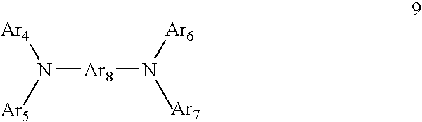
In some embodiments, the triarylamine material preferably incorporates one or more arylenediamine linkages of the formula 9:
Figure US07166010-20070123-C00004

where Ar4, Ar5, Ar6, Ar7, and Ar8 are substituted or unsubstituted aryl or arylene groups and where, optionally, the arylenediamine linkage(s) is/are coupled to other portions of the compound through one or more of the arylene functional groups, if present. One preferred arylenediamine linkage is a phenylenediamine linkage where Ar8 is a phenylene group. Examples of suitable compounds of this type include those compounds illustrated in Formulas 10–12:
Figure US07166010-20070123-C00005

where each R2 is independently alkyl or aryl and each R3 and R4 is independently H, alkyl, aryl, alkoxy, aryloxy, arylthio, alkylthio, halo, or —NRaRb, where Ra and Rb are aryl or alkyl. Each aryl or alkyl portion of any of these substituents can be substituted or unsubstituted. In some embodiments, one of the following conditions applies: all of the R3 and R4 substituents are the same; all of the R3 substituents are the same; all of the R4 substituents are the same; or all of the R3 substituents and all of the R4 substituents are the same, but R3 and R4 are different.
Specific examples of suitable compounds of this type include 4,4′,4″-tris(N,N-diphenylamino)triphenylamine (TDATA) (Formula 13), 4,4′,4″-tris(N-3-methylphenyl-N-phenylamino)triphenylamine (MTDATA) (Formula 14), 4,4′,4″-tris(carbozol-9-yl)triphenylamine (TCTA) (Formula 15), 4,4′,4″-tris(N-naphthyl-N-phenylamino)triphenylamine (2-TNATA) (Formula 16):
Figure US07166010-20070123-C00006
Figure US07166010-20070123-C00007

Another example is Formula 17 where each X is independently O or S (and preferably all of the X substituents are the same).
Figure US07166010-20070123-C00008
As an alternative to small molecule triarylamine materials, polymeric materials with triarylamine moieties can be used. The triarylamine moieties can be in the backbone of the polymeric material, can be pendent groups extending from the backbone of the polymeric material, or both. Polymers with triarylamine moieties in the backbone include, for example, the polymers of Formulas 18, 19, 20, and 21:
Figure US07166010-20070123-C00009

where R3 and R4 are independently H, alkyl, aryl, alkoxy, aryloxy, arylthio, alkylthio, halo, or —NRaRb, where Ra and Rb are aryl or alkyl, Ar9 is aryl or arylene, CM is one or more comonomers, n is an integer of three or greater and preferably 10 or greater, and m is an integer of zero or greater. Each aryl or alkyl portion of any of these substituents can be substituted or unsubstituted. Suitable comonomers, CM, include, for example, another triarylamine-containing monomer such as those illustrated in Formulas 18–21 or 33–34 below, arylene (including substituted or unsubstituted para- or meta-phenylene), substituted or unsubstituted styrene comonomers, derivatized carbazole comonomers (such as N-alkyl carbazole or N-aryl carbazole, for example, the comonomers as illustrated in Formulas 29 and 32), ether-and polyether-linked comonomers, carbonate comonomers, urethane-linked comonomers, thioether-linked comonomers, ester-linked comonomers, and imide-and amide-linked comonomers. Examples of such comonomers include, but are not limited to, —O—(CnH2nO)— and —Ar10—O—(CnH2nO)—Ar11— where Ar10 and Ar11 are arylene.
In some instances, the comonomer contains one or more photo- or thermocrosslinking functional groups, such a benzocyclobutene (Formula 22) or acrylate or methacrylate groups, such as, for example, the acrylate group of Formula 23.
Figure US07166010-20070123-C00010

Other examples of cross-linkable moieties are described in, for example, PCT patent application Publication No. WO 97/33193, incorporated herein by reference. In some embodiments, the polymers containing such cross-linkable moieties are selected to crosslink under relatively mild photochemical or thermal conditions. For example, thermal crosslinking may occur at 100 to 150° C. Alternatively, UV-visible radiation in the range of 300 to 700 nm might be used to crosslink the polymers.
Typically the comonomer is copolymerized with the triarylamine-containing monomer unit. However, in some instances, the comonomer can be coupled to the triarylamine-containing monomer unit prior to polymerization. Such a polymer might not be considered a copolymer, but rather a homopolymer with the coupled triarylamine-containing unit/comonomer unit as the basic monomer unit of the polymer. Examples of such polymers are illustrated by Formulas 24–27.
Figure US07166010-20070123-C00011
Specific examples of the polymers of Formulas 24–27 include the polymers of Formulas 28–32:
Figure US07166010-20070123-C00012
Figure US07166010-20070123-C00013

In Formulas 29–32, the comonomer unit is coupled to the triarylamine moiety-containing monomer unit in such a way that the two monomer units alternate in the polymer.
Formulas 33 and 34 illustrate polymers with triarylamine pendent groups:
Figure US07166010-20070123-C00014

where R3, R4, and R5 are independently H, alkyl, aryl, alkoxy, aryloxy, arylthio, alkylthio, halo, or —NRaRb, where Ra and Rb are aryl or alkyl, CM is one or more comonomers, n is an integer of three or greater and preferably 10 or greater, and m is an integer of zero or greater. Each aryl or alkyl portion of any of these substituents can be substituted or unsubstituted. Suitable comonomers, CM, include, for example, another triarylamine-containing monomer containing one or more chain polymerizable moieties, arylenes (including substituted or unsubstituted para-or meta-phenylene) with one or more chain polymerizable moieties, derivatized carbazole comonomers (such as N-vinyl carbazole), carbonate comonomers, urethane-linked comonomers, thioether-linked comonomers, ester-linked comonomers, imide-and amide-linked comonomers, substituted or unsubstituted styrene comonomers, (meth)acrylate comonomers of, for example, C1–C12 alcohols, diene comonomers such as, for example, butadiene, isoprene and 1,3 cyclohexadiene, and other chain-polymerizable comonomers.
Typically the comonomer is copolymerized with the triarylamine-containing monomer unit. However, in some instances, the comonomer can be coupled to the triarylamine-containing monomer unit prior to polymerization. Such a polymer might not be considered a copolymer, but rather a homopolymer with the coupled triarylamine-containing unit/comonomer unit as the basic monomer unit of the polymer. One example is illustrated as Formula 35.
Figure US07166010-20070123-C00015
It will be understood that the pendent groups can also extend from backbone moieties other than the ethylene moieties illustrated in Formulas 33 and 34. Examples of other backbone units from which the triarylamine pendent groups can extend include, for example, alkylene (such as propylene, butylenes, isoprene, or 1,3-cyclohexadiene), silane, arylenes (including substituted or unsubstituted para- or meta-phenylene), derivatized carbazole monomers (as illustrated in Formulas 29 and 32), carbonate monomers, urethane-linked monomers, thioethers-linked monomers, ester-linked monomers, imide- and amide-linked monomers, substituted and unsubstituted styrene monomers, and (meth)acrylate monomers. The triarylamine may not be directly attached to the backbone, but may be separated from the backbone by a spacer group such as, for example, an alkylene group (e.g., methylene or ethylene), alkenylene (e.g., —(CH═CH)n—, n=1–6), alkynylene (e.g., —(C≡C)n—, n=1–6), arylene, an alkyl ether (e.g., —CH2—O—) group, or any combination of these groups.
Specific examples of suitable polymers with pendent triarylamine groups include, for example, the polymers of Formulas 36–38:
Figure US07166010-20070123-C00016

where each R3, R4, R5, R6, and R7 is independently H, alkyl, aryl, alkoxy, aryloxy, arylthio, alkylthio, halo, or —NRaRb, where Ra and Rb are aryl or alkyl. Each aryl or alkyl portion of any of these substituents can be substituted or unsubstituted. In some embodiments, one or more of the following conditions applies: all of the R3, R4, and R5 substituents are the same; all of the R3 substituents are the same; all of the R4 substituents are the same; all of the R5 substituents are the same; all of the R7 substituents are the same; or all of the R3 substituents and all of the R4 substituents are the same, but R3 and R4 are different. For example, R3, R5, R6, and R7 can be H and R4 can be methyl in any of Formulas 36–38.
Unless otherwise indicated, the term “alkyl” includes both straight-chained, branched, and cyclic alkyl groups and includes both unsubstituted and substituted alkyl groups. Unless otherwise indicated, the alkyl groups are typically C1–C20. Examples of “alkyl” as used herein include, but are not limited to, methyl, ethyl, n-propyl, n-butyl, n-pentyl, isobutyl, and isopropyl, and the like.
Unless otherwise indicated, the term “aryl” refers to monovalent unsaturated aromatic carbocyclic radicals having one to fifteen rings, such as phenyl or bipheynyl, or multiple fused rings, such as naphthyl or anthryl, or combinations thereof. Examples of aryl as used herein include, but are not limited to, phenyl, 2-naphthyl, 1-naphthyl, biphenyl, 2-hydroxyphenyl, 2-aminophenyl, 2-methoxyphenyl and the like.
Unless otherwise indicated, the term “arylene” refers to divalent unsaturated aromatic carbocyclic radicals having one to fifteen rings, such as phenylene, or multiple fused rings, such as fluorene, naphthylene or anthrylene, or combinations thereof. Examples of “arylene” as used herein include, but are not limited to, benzene-1,2-diyl, benzene-1,3-diyl, benzene-1,4-diyl, naphthalene-1,8-diyl, anthracene-1,4-diyl, fluorene, phenylenevinylene, phenylenedivinylene, and the like.
Unless otherwise indicated, the term “alkoxy” refers to the functional group —OR where R is a substituted or unsubstituted alkyl group. Unless otherwise indicated, the alkyl group is typically C1–C20. Examples of “alkoxy” as used herein include, but are not limited to, methoxy, ethoxy, n-propoxy, and 1-methylethoxy, and the like.
Unless otherwise indicated, the term “aryloxy” refers to the functional group —OAr where Ar is a substituted or unsubstituted aryl group. Examples of “aryloxy” as used herein include, but are not limited to, phenyloxy, naphthyloxy, and the like.
Suitable substituents for substituted alkyl, aryl, and arylene groups include, but are not limited to, alkyl, alkylene, aryl, arylene, heteroaryl, heteroarylene, alkenyl, alkenylene, —NRR′, F, Cl, Br, I, —OR, —SR, cyano, nitro, —COOH, and —COO-alkyl where R and R′ are independently hydrogen, alkyl, or aryl.
Unless otherwise indicated, the term “halo” includes fluoro, chloro, bromo, and iodo.
Unless otherwise indicated, the term “polymer” includes homopolymers and copolymers including block copolymers and random copolymers.
In addition to the triarylamine material, the buffer layer also includes an electron acceptor material to improve electron transport. Preferably, such compounds have relatively high electron affinity and relatively low energy of the lowest unoccupied molecular orbital (LUMO). Suitable electron acceptor materials include electron deficient compounds such as, for example, tetracyanoquinodimethane and derivatives, thiopyranylidines, polynitrofluorenones, tetracyanoethylene (TCNE), chloranil, and other compounds commonly used as electron acceptors in charge transfer materials and electrophotography. Specific examples of electron acceptor materials include tetracyanoquinodimethane (TCNQ) (Formula 39), tetrafluoro-tetracyanoquinodimethane (F4-TCNQ) (Formula 40), tetracyanoethylene, chloranil, 2-(4-(1-methylethyl)phenyl-6-phenyl-4H-thiopyran-4-ylidene)-propanedinitrile-1,1-dioxyide (PTYPD) (Formula 41), and 2,4,7-trinitrofluorenone (Formula 42).
Figure US07166010-20070123-C00017

Preferably, the electron acceptor material is soluble in one or more organic solvents, more preferably, one or more organic solvents in which the triarylamine material is also soluble. Typically, the electron donor material is present in the buffer layer in the range of 0.5 to 20 wt. % of the triarylamine material. In some embodiments, the electron donor material is present in the buffer layer in the range of 1 to 5 wt. % of the triarylamine material.
The buffer layer optionally includes a polymeric binder. The polymeric binder can include inert or electroactive polymers or combinations thereof. Suitable polymers for the polymeric binder include, for example, polystyrene, poly(N-vinyl carbazole), polyfluorenes, poly(para-phenylenes), poly(phenylenevinylenes), polycarbonates, polyimides, polyolefins, polyacrylates, polymethacrylates (for example, poly(methylmethacrylate)), polyethers, polysulfones, polyether ketones, and copolymers or mixtures thereof. If the triarylamine material includes a triarylamine-containing polymer, that polymer can act as or in cooperation with a polymeric binder, if desired. If used, the polymeric binder is typically provided in the range of 20 to 150 wt. %, preferably 70 to 120 wt. %, of the triarylamine material.
In some embodiments, the polymeric binder can be photochemically or thermally crosslinked with itself or with other components in the buffer layer. Accordingly, a thermochemical or photochemical crosslinking agent, such as, for example, 2,6-bis(4-azidobenzylidene)-4-methylcyclohexanone, can optionally be included in the buffer layer. Crosslinking can be desirable for one or more purposes, such as decreasing the migration of buffer layer components out of the buffer layer, decreasing the migration of other materials into the buffer layer, increasing thermal stability, increasing mechanical stability, increasing morphological stability, increasing buffer layer stability, and increasing layer integrity, particularly during further solution processing. Crosslinking the buffer layer can also facilitate manufacture of a device by providing a buffer layer upon which other layers can be solution coated or cast with substantially less concern about dissolving the buffer layer.
The buffer layer can optionally include a color converting material. This material can be a luminescent or non-luminescent organic, organometallic, or inorganic compound or combinations thereof. The color converting material changes the color of electroluminescence from an emitting layer by selective absorption of light or by absorption of light and re-emission of the light in a different spectral range. Suitable materials include, for example, dyes, pigments, and nanoparticles. Examples of suitable non-luminescent and luminescent dyes include: azo dyes (e.g. C.I. Direct Green 26 and others), anthraquinone dyes (e.g. C.I. Reactive Blue 4 and others), indigoid dyes (e.g. Tyrian Purple and others), triphenylmethane-based dyes (e.g. Eosin and others), coumarin dyes (e.g. Coumarin 6 and others), metal porphyrins (e.g. platinum [II] octaethylporphyrin and others), cyclometalated transition metal complexes (e.g. iridium tris(2-phenylpyridine) and others), and other dyes including those discussed in H. Zollinger, Color Chemistry, 1991, VCH Publishers: New York, and The Chemistry and Application of Dyes, Ed. By D. R. Waring and G. Halls, 1990, Plenum Press: New York, both of which are incorporated herein by reference. Examples of nanoparticles suitable for color conversion can be found in M. Bruchez et al., Science 281, 2013 (1998), incorporated herein by reference. The color converting material can be polymeric with color converting moieties in the backbone, on pendant chains, or both. The color converting material, if used, is typically included in the buffer layer in an amount in the range of 0.1 to 100 wt. %, preferably 0.1 to 10 wt. %, of the triarylamine material.
The buffer layer can also optionally include scattering material, such as small particles, nanocrystals, or clusters. Examples of suitable materials include clays, oxides, metals, and glasses. Specific examples of suitable materials include titania, alumina and silica powders having a mean particle size of approximately 0.05 to 0.2 microns, and added to the buffer layer composition in a concentration of from 0.1 to 20% by weight, and preferably from about 1–5% by weight.
The buffer layer 254 is formed by solution coating the material of the buffer layer onto the substrate 250. After formation of the buffer layer 254, additional layers, such as the hole transport layer 260 or emission layer 256, can be formed on the buffer layer by a variety of techniques including, for example, solution coating, physical or chemical vapor deposition, and thermal transfer, including light-induced thermal transfer as described below.
An organic solvent is used to make the solution for the buffer layer. Examples of suitable organic solvents include carbon tetrachloride, toluene, chloroform, 1,2-dichloroethane, 1,2-dichlorobenzene, tetrahydrofuran, pyridine, and the like. The remaining materials of the buffer layer are typically dispersible or, preferably, soluble in the organic solvent.
In some conventional device formation methods, layers are formed using solutions of components in water. A drawback of these methods is that some of the device materials are degraded in the presence of water or irreversible physical changes may occur leading to device degradation. Thus, if a layer is formed using a water solution, the water generally must be completely removed. On the other hand according to the invention, organic solvents can be chosen that are easier to remove or do not degrade materials in the device or both.
In other conventional device formation methods, the materials of a layer are disposed by vapor deposition. A number of materials are difficult to accurately and consistently deposit by vapor deposition methods. Included in these materials are a variety of polymers and ionic compounds. Thus, it can be difficult to deposit materials such as a polymeric binder and cross-linking agent using vapor deposition techniques. In addition, the consistency and uniformity of a vapor deposited composition becomes increasingly difficult when the composition contains multiple components. On the other hand according to the invention, forming a buffer layer by solution coating can facilitate the use of materials such as polymeric binders, polymeric triarylamine materials, cross-linking agents, dyes, pigments, scattering particles, and so on. In addition, the coating technique permits the use of multi-component systems when all of the components are soluble or dispersible in the solvent.
As an alternative to solution coating the buffer layer material directly onto the substrate or depositing the buffer layer material using ink jet techniques, the buffer layer material can be coated onto a donor sheet and then transferred by techniques such as thermal transfer to the substrate. This can be particularly useful for patterning the buffer layer onto the substrate. For example, the buffer layer material can be selectively transferred from the donor sheet to the substrate according to a pattern by selective application of, for example, light or heat to the donor sheet. This can be useful, for example, to pattern individual buffer layers with a different color converting materials (or lack of color converting material) onto the substrate. Thus, a full-color display could be formed using, for example, three different buffer layers with three different color converting materials (or two different color converting materials and the third buffer layer lacking a color converting material). Other methods of selectively patterning color converting materials in buffer layer(s) include, for example, thermal diffusion of the color converting material, inkjet transfer of the buffer material with (or without) color converting materials onto the substrate, and selective photobleaching.
Suitable thermal transfer methods for transferring a buffer layer or other device layers to the substrate or onto a previously-formed buffer layer include, for example, thermal head transfer methods and light-induced thermal transfer methods. The presence of the buffer layer on the substrate can, at least in some instances, facilitate the transfer of other layers to the substrate by these methods. Materials, layers, or other structures can be selectively transferred from the transfer layer of a donor sheet to a receptor substrate by placing the transfer layer of the donor element adjacent to the receptor and selectively heating the donor element. For example, the donor element can be selectively heated by irradiating the donor element with imaging radiation that can be absorbed by light-to-heat converter material disposed in the donor, often in a separate light-to-heat conversion (LTHC) layer, and converted into heat. Examples of such methods, donor elements and receptors, as well as articles and devices that can be formed using thermal transfer, can be found in U.S. Pat. Nos. 5,521,035, 5,691,098, 5,693,446, 5,695,907, 5,710,097, 5,725,989, 5,747,217, 5,766,827, 5,863,860, 5,897,727, 5,976,698, 5,981,136, 5,998,085, 6,057,067, 6,099,994, 6,114,088, 6,140,009, 6,190,826, 6,194,119, 6,221,543, 6,214,520, 6,221,553, 6,228,543, 6,228,555, 6,242,152, 6,270,934, and 6,270,944 and PCT patent applications Publication Nos. WO 00/69649 and WO 01/39986 and U.S. patent applications Ser. Nos. 09/662,845, 09/662,980, 09/844,100, and 09/931,598, all of which are incorporated herein by reference. The donor can be exposed to imaging radiation through the donor substrate, through the receptor, or both. The radiation can include one or more wavelengths, including visible light, infrared radiation, or ultraviolet radiation, for example from a laser, lamp, or other radiation source.
Other selective heating methods can also be employed, such as using a thermal print head or using a thermal hot stamp (e.g., a patterned thermal hot stamp such as a heated silicone stamp that has a relief pattern that can be used to selectively heat a donor). Thermal print heads or other heating elements may be particularly suited for making lower resolution patterns of material or for patterning elements whose placement need not be precisely controlled.
Material from the transfer layer can be selectively transferred to a receptor in this manner to imagewise form patterns of the transferred material on the receptor. In many instances, thermal transfer using light from, for example, a lamp or laser, to patternwise expose the donor can be advantageous because of the accuracy and precision that can often be achieved. The size and shape of the transferred pattern (e.g., a line, circle, square, or other shape) can be controlled by, for example, selecting the size of the light beam, the exposure pattern of the light beam, the duration of directed beam contact with the donor sheet, or the materials of the donor sheet. The transferred pattern can also be controlled by irradiating the donor element through a mask.
Transfer layers can also be transferred from donor sheets without selectively transferring the transfer layer. For example, a transfer layer can be formed on a donor substrate that, in essence, acts as a temporary liner that can be released after the transfer layer is contacted to a receptor substrate, typically with the application of heat or pressure. Such a method, referred to as lamination transfer, can be used to transfer the entire transfer layer, or a large portion thereof, to the receptor.
A donor sheet for light-induced thermal transfer can include, for example, a donor substrate, an optional underlayer, an optional light-to-heat conversion (LTHC) layer, an optional interlayer, and a transfer layer. The donor substrate can be a polymer film or any other suitable, preferably transparent, substrate. The donor substrate is also typically selected from materials that remain stable despite heating of one or more layers of the donor. However, the inclusion of an underlayer between the substrate and an LTHC layer can be used to insulate the substrate from heat generated in the LTHC layer during imaging.
The underlayer can include materials that impart desired mechanical or thermal properties to the donor element. For example, the underlayer can include materials that exhibit a low value for the mathematical product of specific heat and density or low thermal conductivity relative to the donor substrate. Such an underlayer may be used to increase heat flow to the transfer layer, for example to improve the imaging sensitivity of the donor. The underlayer can also include materials for their mechanical properties or for adhesion between the substrate and the LTHC.
An LTHC layer can be included in donor sheets of the present invention to couple irradiation energy into the donor sheet. The LTHC layer preferably includes a radiation absorber that absorbs incident radiation (e.g., laser light) and converts at least a portion of the incident radiation into heat to enable transfer of the transfer layer from the donor sheet to the receptor.
An optional interlayer can be disposed between the LTHC layer and transfer layer. The interlayer can be used, for example, to minimize damage and contamination of the transferred portion of the transfer layer and may also reduce distortion in the transferred portion of the transfer layer. The interlayer can also influence the adhesion of the transfer layer to the rest of the donor sheet. Typically, the interlayer has high thermal resistance. Preferably, the interlayer does not distort or chemically decompose under the imaging conditions, particularly to an extent that renders the transferred image non-functional. The interlayer typically remains in contact with the LTHC layer during the transfer process and is not substantially transferred with the transfer layer.
The interlayer can provide a number of benefits, if desired. The interlayer can be a barrier against the transfer of material from the light-to-heat conversion layer. It can also modulate the temperature attained in the transfer layer so that thermally unstable materials can be transferred. For example, the interlayer can act as a thermal diffuser to control the temperature at the interface between the interlayer and the transfer layer relative to the temperature attained in the LTHC layer. This can improve the quality (i.e., surface roughness, edge roughness, etc.) of the transferred layer. The presence of an interlayer can also result in improved plastic memory in the transferred material.
The thermal transfer layer includes the buffer material to form the buffer layer, if desired, or appropriate materials to form other layers depending on the desired thermal transfer. For example, other layers of the device, such as the hole transport layer or the emission layer, can be transferred onto the substrate or onto the buffer layer or other layers disposed on the substrate by these methods. Such transfer can be sequential using multiple donor sheets or, in some embodiments, multiple layers can be transferred using a single donor sheet with the transfer layer having individual sublayers.
The present invention contemplates light emitting OEL displays and devices. In one embodiment, OEL displays can be made that emit light and that have adjacent devices that can emit light having different color. For example, FIG. 5 shows an OEL display 300 that includes a plurality of OEL devices 310 disposed on a substrate 320. Adjacent devices 310 can be made to emit different colors of light.
The separation shown between devices 310 is for illustrative purposes only. Adjacent devices may be separated, in contact, overlapping, etc., or different combinations of these in more than one direction on the display substrate. For example, a pattern of parallel striped transparent conductive anodes can be formed on the substrate followed by a striped pattern of a hole transport material and a striped repeating pattern of red, green, and blue light emitting LEP layers, followed by a striped pattern of cathodes, the cathode stripes oriented perpendicular to the anode stripes. Such a construction may be suitable for forming passive matrix displays. In other embodiments, transparent conductive anode pads can be provided in a two-dimensional pattern on the substrate and associated with addressing electronics such as one or more transistors, capacitors, etc., such as are suitable for making active matrix displays. Other layers, including the light emitting layer(s) can then be coated or deposited as a single layer or can be patterned (e.g., parallel stripes, two-dimensional pattern commensurate with the anodes, etc.) over the anodes or electronic devices. Any other suitable construction is also contemplated by the present invention.
In one embodiment, display 300 can be a multiple color display. As such, it may be desirable to position optional polarizer 330 between the light emitting devices and a viewer, for example to enhance the contrast of the display. In exemplary embodiments, each of the devices 310 emits light. There are many displays and devices constructions covered by the general construction illustrated in FIG. 3. Some of those constructions are discussed as follows.
OEL backlights can include emissive layers. Constructions can include bare or circuitized substrates, anodes, cathodes, hole transport layers, electron transport layers, hole injection layers, electron injection layers, emissive layers, color changing layers, and other layers and materials suitable in OEL devices. Constructions can also include polarizers, diffusers, light guides, lenses, light control films, brightness enhancement films, and the like. Applications include white or single color large area single pixel lamps, for example where an emissive material is provided by thermal stamp transfer, lamination transfer, resistive head thermal printing, or the like; white or single color large area single electrode pair lamps that have a large number of closely spaced emissive layers patterned by laser induced thermal transfer; and tunable color multiple electrode large area lamps.
Low resolution OEL displays can include emissive layers. Constructions can include bare or circuitized substrates, anodes, cathodes, hole transport layers, electron transport layers, hole injection layers, electron injection layers, emissive layers, color changing layers, and other layers and materials suitable in OEL devices. Constructions can also include polarizers, diffusers, light guides, lenses, light control films, brightness enhancement films, and the like. Applications include graphic indicator lamps (e.g., icons); segmented alphanumeric displays (e.g., appliance time indicators); small monochrome passive or active matrix displays; small monochrome passive or active matrix displays plus graphic indicator lamps as part of an integrated display (e.g., cell phone displays); large area pixel display tiles (e.g., a plurality of modules, or tiles, each having a relatively small number of pixels), such as may be suitable for outdoor display used; and security display applications.
High resolution OEL displays can include emissive layers. Constructions can include bare or circuitized substrates, anodes, cathodes, hole transport layers, electron transport layers, hole injection layers, electron injection layers, emissive layers, color changing layers, and other layers and materials suitable in OEL devices. Constructions can also include polarizers, diffusers, light guides, lenses, light control films, brightness enhancement films, and the like. Applications include active or passive matrix multicolor or full color displays; active or passive matrix multicolor or full color displays plus segmented or graphic indicator lamps (e.g., laser induced transfer of high resolution devices plus thermal hot stamp of icons on the same substrate); and security display applications.
EXAMPLES
All chemicals are available from Aldrich Chemical Co., Milwaukee, Wis., unless otherwise indicated.
Preparation of ITO Substrates
For Examples 1–13, ITO substrates were prepared as follows: ITO (indium tin oxide) glass substrates (Applied Films Corporation, CO; ca. 25 Ω/sq.) were rinsed in acetone (Aldrich Chemical Company), dried with nitrogen, and rubbed with TX1010 Vectra Sealed-Border Wipers (ITW Texwipe, Upper Saddle River, N.J.) soaked in methanol (Aldrich Chemical Company, Milwaukee, Wis.), after which they were subjected to oxygen plasma treatment for four minutes at 200 mT (about 27 Pa) base oxygen pressure and output power of 50 W in Technics Micro Reactive Ion Etcher, Series 80 (K&M Company, CA). The OLED's described below were generally 1 to 1.5 cm2 in size.
Comparative Example 1 and Examples 1–3 Buffer Layers Containing of Triarylamine Materials with Electrically Inert Polymers
This Example describes the formation of OLEDs having a solution-processed hole-injecting buffer layer incorporating 4,4′,4″-tris(N-3-methylphenyl-N-phenylamino)triphenylamine (MTDATA) as a triarylamine material, polystyrene (PS) as an electrically inert polymer binder, and tetrafluoro-tetracyanoquinodimethane (F4-TCNQ) or tetracyanoquinodimethane (TCNQ) as an electron accepting dopant material.
The OLED is prepared by vapor depositing, onto an ITO substrate with a buffer layer, 20 nm of N,N′-bis(naphthan-2-yl)-N,N′-bis(phenyl)benzidine (NPD, H.W. Sands Corp., Jupiter, Fla.), followed by 30 nm of aluminum tris(8-hydroxyquinolate) (AlQ, H.W. Sands Corp, Jupiter, Fla.) doped with ca. 1 wt. % of green-emitting Coumarin 545T (C545T, Eastman Kodak Co., Rochester, N.Y.), and followed by 20 nm of AlQ. The OLED was capped with a cathode composed of ca. 0.7 nm of lithium fluoride (LiF, Alfa Aesar Co., Ward Hill, Mass.) and 200 nm of aluminum (Al, Alfa Aesar Co., Ward Hill, Mass.). In this OLED construction, the NPD layer acts as a hole-transport layer and electron-blocking layer, the layer of AlQ doped with C545T (AlQ:C545T) acts as a light emitting layer, and the layer of AlQ acts as an electron injection and transport layer. These OLED constructions are further referred to as “/NPD/AlQ:C545T/AlQ/LiF/Al”.
All organic and cathode layers except the buffer layers were fabricated in a standard vacuum-deposition procedure at a base vacuum of ca. 10−7 to 10−5 torr (about 10−5 to 10−3 Pa) with evaporation rates of 0.05–0.2 nm/s for organic materials, 0.05 nm/s for LiF, and 1.5–2 nm/s for Al.
In Comparative Example 1, polypyrrole (PPY, Aldrich Chemical Co.) was used as a control hole-injecting buffer layer for purposes of comparison of the OLED behavior of the devices deposited onto PPY and onto doped triarylamine-based buffer layers. PPY was spun-coat from its water suspension after filtering the suspension through 0.2 μm Nylon microfilters, followed by annealing under nitrogen gas flow at 110° C. for ca. 15 min.
In Examples 1–4, OLEDs with buffer layers containing MTDATA, PS, and TCNQ were prepared and their performance evaluated along with that of the control PPY-based OLEDs. MTDATA, PS, and TCNQ were purchased from HWSands Corp. (Jupiter, Fla.), Polysciences Inc. (Eppelheim, Germany), and TCI America (Portland, Oreg.), respectively. The buffer layers were spun-coat from their ca. 1.5 wt. % solutions in toluene at the spin-rate of 2000 RPM (about 33 s−1) to form ca. 90 nm thick films on the ITO coated substrates. The device structures are glass-ITO/buffer layer/NPD/AlQ:C545T/AlQ/LiF/Al. The buffers layers for the Examples are:
Comparative Example 1: PPY
Example 1: 31 wt. % PS, 62 wt. % MTDATA, and 7 wt. % TCNQ
Example 2: 47 wt. % PS, 46 wt. % MTDATA, and 7 wt. % TCNQ
Example 3: 62 wt. % PS, 31 wt. % MTDATA, and 7 wt. % TCNQ
No short-circuiting was observed in any of the studied electroluminescent lamps. For Examples 1–3, the OLEDs showed high operational efficiency and low operational voltages, with operational voltages decreasing with increasing triarylamine concentration.
Examples 5–6 Buffer Layers Containing Triarylamines and an Electroactive Polymer Binder
High bandgap hole-transporting poly(N-vinylcarbazole) (PVK, Polymer Source Inc., Dorval, Quebec) having relatively high oxidation potential (ca. 1V vs. SCE) and low hole mobility (ca. 10−6–10−5 cm2/V*s (about 10−1–10−9 m2 V s)) was used as an electroactive binder in the following buffer compositions: a) 60 wt. % PVK and 40 wt. % MTDATA, and b) 56 wt. % PVK, 37 wt. % MTDATA, and 7 wt. % F4-TCNQ. These buffer layers were spun-coat from their ca. 1.5% wt. solutions in toluene at the spin-rate of 2000 RPM (about 33 s−1) to form ca. 90 nm thick films on the ITO coated substrates.
OLED devices were made as described above for Comparative Example 1 and Examples 1–3, except that the buffer layers corresponded to:
Example 5: 60 wt. % PVK and 40 wt. % MTDATA
Example 6: 56 wt. % PVK, 37 wt. % MTDATA, and 7 wt. % F4-TCNQ.
No short-circuiting was observed in any of the studied electroluminescent lamps. Luminance-voltage-current density screening of the OLEDs indicated that high efficiencies can be obtained in the composition including triarylamine-based buffers along with low operational voltages. Doping the PVK:MTDATA blend with F4-TCNQ significantly lowered the operational voltage of the OLEDs. Operational lifetime studies on the triarylamine-based compositions, in which the OLEDs were driven at a constant current of ca. 1.8 mA/cm2 (about 18 A/m2) under inert atmosphere, show that projected operation lifetimes of these OLEDs extend into 103–104 hours range at an initial luminance of several hundred Cd/m2.
Examples 7 and 8 Buffer Layers Containing Copolymers with Triarylamine Moieties Pendant to a Polyolefin Backbone
In this Example, doped triarylamine buffer layers based on copolymers incorporating triarylamine moieties as a functionality pendant to a polyolefin backbone were incorporated into OLEDs.
A block co-polymer of styrene with diphenylaminostyrene (PS-pDPAS), having approximately 6:1 molar ratio of the monomers was synthesized and screened as a triarylamine-containing polymer.
All materials are available from Aldrich Chemical Co., Milwaukee, Wis., with the exception of p-diphenylaminostyrene, and as where noted. This monomer was synthesized by a preparation similar to that described by G. N. Tew, M. U. Pralle, and S. I. Stupp in Angew. Chem. Int. Ed., 2000, 39, 517, incorporated herein by reference.
Synthesis of p-diphenylaminostyrene
To a mixture of 4-(diphenylamino)benzaldehyde (20.06 g, 73 mmol, Fluka Chemical Co., Milwaukee, Wis.), methyltriphenyl phosphonium bromide (26.22 g, 73 mmol) and dry tetrahydrofuran (450 mL) under nitrogen was added a 1M solution of potassium t-butoxide in tetrahydrofuran (80 mL, 80 mmol) over 5 minutes. The mixture was stirred for 17 hours at room temperature. Water (400 mL) was added and the tetrahydrofuran was removed under reduced pressure. The mixture was extracted with ether, and the combined organic layers were dried over MgSO4 and concentrated under vacuum. The crude solid was purified by column chromatography on silica gel using a 50/50 mixture of methylene chloride and hexane to give a yellow solid that was further recrystallized once from hexane (15.37 g, 78%).
Synthesis of Block Co-polymer of Styrene with Diphenylaminostyrene (PS-pDPAS)
A round-bottom glass reactor was baked out under vacuum at 200° C. for 2 hours, then allowed to cool. The reactor was filled with dry nitrogen. Subsequently, 71.8 g of cyclohexane and 4.4 mL of tetrahydrofuran (THF) were added to the reactor by syringe. The THF was distilled from sodium/benzophenone solution under nitrogen prior to use, in order to scavenge water and oxygen. The cyclohexane was dried by passage through activated basic alumina, followed by sparging with nitrogen gas for 30 minutes prior to use. After addition of the solvents, the reaction flask was cooled to 3° C. in an ice water bath, after which 0.02 mL of styrene was added to the reactor. The styrene had previously been passed through activated basic alumina to remove inhibitors and water, and sparged with nitrogen gas to remove oxygen. A solution of s-butyllithium in cyclohexane (0.4 mL, 1.3 mol/L) was subsequently added to the reactor. The solution immediately turned orange, characteristic of the formation of polystyryl anion. After stirring at 3° C. for 2 hours, a solution of p-diphenylaminostyrene (1.61 g) in cyclohexane (20 mL) was added to the reactor by cannula. This solution had previously been degassed by repeatedly freezing it with liquid nitrogen and exposing it to vacuum. The solution was stirred overnight while warming to room temperature. The reaction was then terminated by addition of methanol, precipitated into a mixture of methanol and isopropanol, and dried under in a vacuum oven overnight, yielding 3.2 g of polymer. The resulting PS-pDPAS block polymer contained 74.1 mol % styrene and 25.9 mol % p-diphenylaminostyrene, based on 13C NMR. The molecular weight of the block copolymer was 7700 g/mol, based on gel permeation chromatography in THF against polystyrene standards.
OLED Preparation
OLEDs were formed as described in the Comparative Example 1 and Examples 1–3 except that the buffer layers were as follows:
Example 7: PS-pDPAS
Example 8: 93 wt. % PS-pDPAS and 7 wt. % F4-TCNQ.
These buffer layers were spun-coat from their ca. 1.5% wt. solutions in toluene at the spin-rate of 2000 RPM (about 33 s−1) to form ca. 90 nm thick films on the ITO coated substrates.
No short-circuiting was observed in any of the studied electroluminescent lamps. Luminance-voltage-current density screening of the OLEDs indicated that high efficiencies and low operational voltages were obtained. Doping PS-pDPAS with F4-TCNQ significantly lowered the operational voltage of the OLEDs.
Comparative Example 2 and Examples 9 and 10 Buffer Layers Containing Conjugated Copolymers with Triarylamine Moieties in the Backbone
This describes the preparation and characterization of an OLED with doped co-polymer based triarylamine hole injecting buffer layers. The buffer layers include PEDT (poly(3,4-ethylenedioxythiophene) available as CH8000 from Bayer AG, Leverkusen, Germany), undoped poly{(9-phenyl-9H-carbazole-3,6-diyl)[N,N′-bis(phenyl-4-yl)-N,N′-bis(4-butylphenyl)benzene-1,4-diamine]} (Cz-triarylamine), and Cz-triarylamine doped with F4-TCNQ. An advantage of using Cz-triarylamine as a triarylamine-containing co-polymer for hole injecting buffer layers lies in the presence of phenylenediamine linkages, which typically cause lower ionization potential (higher energy of the highest occupied molecular orbital). This provides favorable conditions for increased conductivity due to doping with electron acceptors (e.g. F4-TCNQ).
3,6-Dibromo-9-phenylcarbazole was made according to M. Park, J. R. Buck, C. J. Rizzo, J. Carmelo. Tetrahedron 119, 54 (42), 12707–12714, incorporated herein by reference. N,N′-bis(4-bromophenyl)-N,N′-bis(4-butylphenyl)benzene-1,4-diamine can be obtained in two steps from 1,4-phenylenediamine as reported in Raymond et al., Polymer Preprints 2001, 42(2), 587–588, incorporated herein by reference. Tricaprylylmethylammonium chloride is available from Aldrich Chemical Company under the trade name Aliquat® 336. All other materials were obtained from Aldrich Chemical Company.
Preparation of 9-Phenyl-3,6-bis(4,4,5,5-tetramethyl-1,3,2-dioxaborolan-2-yl)-9H-carbazole
A 2 L flask was charged with 600 mL dry THF and 3,6-dibrimo-9-phenylcarbazole (60 g, 0.15 mole). This was cooled to −78° C. with an acetone-dry ice bath. n-Butyllithium (138 mL of a 2.5M solution in hexanes, 0.34 mole) was added drop-wise via syringe. The reaction was stirred for 20 minutes and then warmed to −50° C. The temperature was reduced to −78° C. and 2-isopropoxy-4,4,5,5-tetramethyl-1,3,2-dioxaborolane (64 g, 0.34 mole) added via syringe at such a rate as to maintain the temperature below −60° C. The reaction was maintained at −78° C. for two hours and then poured into an aqueous solution of ammonium acetate (90 g in 2100 mL water). The layers were phase separated and the aqueous phase extracted with methyl tert-butyl ether (2×200 mL). The combined organic phase and extracts were washed with brine (2×200 mL) and dried over magnesium sulfate. Concentration and re-crystallization of the solid obtained form acetone gave pure 9-phenyl-3,6-bis(4,4,5,5-tetramethyl-1,3,2-dioxaborolan-2-yl)-9H-carbazole (12 g, 16% yield).
Preparation of Poly{(9-phenyl-9H-carbazole-3,6-diyl)[N,N′-bis(phenyl-4-yl)-N,N′-bis(4-butylphenyl)benzene-1,4-diamine]} (Cz-triarylamine- Formula 32 above)
In a 50 mL round bottomed flask fitted with a rubber septum and reflux condenser were introduced 9-phenyl-3,6-bis(4,4,5,5-tetramethyl-1,3,2-dioxaborolan-2-yl)-9H-carbazole (0.79 g, 1.59 mmole, 5 equivalents), N,N′-bis(4-bromophenyl)-N,N′-bis(4-butylphenyl)benzene-1,4-diamine (0.65 g, 0.952 mmol, 3 equivalents), Aliquat® 336 (0.16 g, 0.405 mmole, 1.28 equivalents), 2M sodium carbonate solution (5.4 mL, 10.8 mmol, 34 equivalents) and 20 mL toluene. This was purged with a stream of nitrogen for 30 min. Under a nitrogen purge, tetrakistriphenylphosphine palladium (0) (10 mg, 0.0.0068 mmole, 0.02 equivalents) was added. The reaction mixture was then refluxed for 16 hrs. A solution of 0.5 g bromobenzene in 5 mL purged toluene was added followed by and a further charge of tetrakistriphenylphosphine paladium (0) (10 mg) and refluxing then continued for a further 16 hrs.
The reaction was then cooled to room temperature and 30 mL water added. The organic layer was separated and washed with water followed by brine. Precipitation into methanol, filtration and vacuum drying of the solid thus obtained gave 0.62 g of the required hole transport polymer. Molecular weight determination by gel permeation chromatography versus polystyrene standards gave Mw 2.39×10³, Mn 1.49×10³ and polydispersity of 1.67
OLED Preparation
OLEDs were formed as described in the Comparative Example 1 and Examples 1–3 except that the buffer layers were as follows:
Comparative Example 2: PEDT
Example 9: Cz-triarylamine
Example 10: 93 wt. % Cz-triarylamine and 7 wt. % F4-TCNQ.
These buffer layers were spun-coat from their ca. 1.5% wt. solutions in toluene at the spin-rate of 2000 RPM (about 33 s−1) to form ca. 90 nm thick films on the ITO coated substrates.
No short-circuiting was observed in any of the studied electroluminescent lamps. Devices with both doped and undoped Cz-triarylamine-based buffer layer showed high external quantum efficiencies. Devices with undoped Cz-triarylamine buffer layer showed noticeably higher operational voltages than those made on PEDT. Upon doping Cz-triarylamine with F4-TCNQ, operational voltages decreased to the level of those observed for PEDT-based LEDs. This indicates that Cz-triarylamine possesses an ionization potential which is low enough for efficient F4-TCNQ doping to increase conductivity in the hole-injecting buffer layer.
Preliminary operation stability studies on devices incorporating Cz-triarylamine buffer layer carried out in the constant current continuous sweep regime at current density levels of ca. 1.8 mA/cm2 (luminance of 100–150 Cd/m2) suggest that Cz-triarylamine-based buffer layers can be used to achieve improved operational lifetime in OLEDs.
Examples 11–13 Absorptive Dye Doped Color Converting Buffer Layers
This Example describes the fabrication of hole-injecting solution-processed buffer layers based on doped triarylamines blended with electroactive polymer binder and blended with color-converting organic dye material in order to tune electroluminescence energy and CIE color coordinates of the OLEDs incorporating such buffer layers.
Three solutions consisting of a) 30 mg poly(vinyl carbazole) (PVK, Aldrich Chemical Co.), 20 mg MTDATA (H. W. Sands Corp., Jupiter, Fla.), 2 mg F4-TCNQ (TCI America, Portland, Oreg.), 3.7 ml CHCl3, b) 30 mg PVK, 20 mg MTDATA, 2 mg F4-TCNQ, 75 mg 1,4-bis(2-methyl-6-ethyl anilino) anthraquinone (Dye), 3.7 ml CHCl3 and, c) 30 mg PVK, 20 mg MTDATA, 2 mg F4-TCNQ, 117 mg 1,4-bis(2-methyl-6-ethyl anilino) anthraquinone (Dye), 3.7 ml CHCl3 were prepared. The Dye can be prepared according to U.S. Pat. No. 5,639,896, incorporated herein by reference and is available as “Amaplast Blue RFC” supplied by “American Aniline Products”, N.Y., N.Y., a unit of Koppers Co., Pittsburgh, Pa. Each solution was then spun coat onto cleaned ITO substrates at 3000 R.P.M. for 30s. A vapor deposited small-molecule OLED with NPD (20 nm, 0.2 nm/s), AlQ (50 nm, 0.1 nm/s), LiF (0.7 nm, 0.05 nm/s), Al (200 nm, 2 nm/s) was sequentially deposited on top in a standard vacuum deposition procedure at 10−6 torr (about 10−4 Pa) as described in Comparative Example 1 and Examples 1–3.
OLEDs were formed as described in the Comparative Example 1 and Examples 1–3 except that the buffer layers were as follows:
Example 11: Solution a) corresponding to 58 wt. % PVK, 38 wt. % MTDATA, and 4 wt. % F4-TCNQ
Example 12: Solution b) corresponding to 24 wt. % PVK, 16 wt. % MTDATA, 2 wt. % F4-TCNQ, and 58 wt. % Dye
Example 13: Solution c) corresponding to 18 wt. % PVK, 12 wt. % MTDATA, 1 wt. % F4-TCNQ, and 69 wt. % Dye.
Devices containing the dye in the buffer layer exhibit a clear change in the electroluminescence spectrum and the corresponding C.I.E coordinates due to selective absorption of the AlQ emission by the dye. CIE color coordinates for two hole-injecting buffer layer compositions containing the studied dye material in different concentrations as well as those for the control device are shown in Table I.
TABLE I
Color Coordinate Shift
Sample CIE (x) CIE (y)
Example 11 0.34 0.55
Example 12 0.20 0.56
Example 13 0.17 0.57
Example 14 Preparation of an OLED Device Using Thermal Transfer
Preparation of a Donor Sheet without a Transfer Layer
A thermal transfer donor sheet was prepared in the following manner:
An LTHC solution, given in Table II, was coated onto a 0.1 mm thick polyethylene terephthalate (PET) film substrate (M7 from Teijin, Osaka, Japan). Coating was performed using a Yasui Seiki Lab Coater, Model CAG-150, using a microgravure roll with 150 helical cells per inch. The LTHC coating was in-line dried at 80° C. and cured under ultraviolet (UV) radiation.
TABLE II
LTHC Coating Solution
Parts by
Component Trade Designation Weight
carbon black pigment Raven 760 Ultra (1) 3.55
polyvinyl butyral resin Butvar B-98 (2) 0.63
acrylic resin Joncryl 67 (3) 1.90
Dispersant Disperbyk 161 (4) 0.32
Surfactant FC-430 (5) 0.09
epoxy novolac acrylate Ebecryl 629 (6) 12.09
acrylic resin Elvacite 2669 (7) 8.06
2-benzyl-2-(dimethylamino)-1-(4- Irgacure 369 (8) 0.82
(morpholinyl)phenyl)butanone
1-hydroxycyclohexyl phenyl ketone Irgacure 184 (8) 0.12
2-butanone 45.31
1,2-propanediol monomethyl ether 27.19
acetate
(1) available from Columbian Chemicals Co., Atlanta, GA
(2) available from Solutia Inc., St. Louis, MO
(3) available from S. C. Johnson & Son, Inc. Racine, WI
(4) available from Byk-Chemie USA, Wallingford, CT
(5) available from Minnesota Mining and Manufacturing Co., St. Paul, MN
(6) available from UCB Radcure Inc., N. Augusta, SC
(7) available from ICI Acrylics Inc., Memphis, TN
(8) available from Ciba-Geigi Corp., Tarrytown, NY
Next, an interlayer solution, given in Table III, was coated onto the cured LTHC layer by a rotogravure coating method using the Yasui Seiki lab coater, Model CAG-150, with a microgravure roll having 180 helical cells per lineal inch. This coating was in-line dried at 60° C. and cured under ultraviolet (UV) radiation.
TABLE III
Interlayer Coating Solution
PARTS BY
COMPONENT WEIGHT
SR 351 HP (trimethylolpropane triacrylate 14.85
ester, available from Sartomer, Exton, PA)
Butvar B-98 0.93
Joncryl 67 2.78
Irgacure 369 1.25
Irgacure 184 0.19
2-butanone 48.00
1-methoxy-2-propanol 32.00

Preparation of Solutions for Receptor
The following solutions were prepared and used in the preparation of layers on the receptor substrate:
  • MTDATA: (4,4′,4″-tris(N-(3-methylphenyl)-N-phenylamino)triphenylamine) (OSA 3939, H. W. Sands Corp., Jupiter, Fla.) 1.0% (w/w) in toluene was filtered and dispensed through a Whatman Puradisc™ 0.45 μm Polypropylene (PP) syringe filter.
  • PVK: Poly(9-vinylcarbazole) (Aldrich Chemical Co., Milwaukee, Wis.) 1.0% (w/w) in toluene was filtered and dispensed through a Whatman Puradisc™ 0.45 μm Polypropylene (PP) syringe filter.
  • F4-TCNQ: Tetrafluorotetracyanoquinodimethane (Tokyo Kasei Kogyo Co., Tokyo, Japan) 0.25% (w/w) in toluene was filtered and dispensed through a Whatman Puradisc™ 0.45 μm Polypropylene (PP) syringe filter.
  • MTDATA/F4-TCNQ: 98/2 w/w % mixture of MTDATA/F4-TCNQ.
  • MTDATA/PVK: 65/35 w/w % mixture of MTDATA/PVK
  • MTDATA/PVK/F4-TCNQ: 64/35/1 w/w/w % mixture of MTDATA/PVK/F4-TCNQ
    Preparation of Receptors
Receptors were formed as follows: ITO(indium tin oxide) glass (Delta Technologies, Stillwater, Minn., less than 100 Ω/square, 1.1 mm thick) was processed using photolithography to provide a patterned ITO structure capable of making an electroluminescent device. The substrate was ultrasonically cleaned in a hot, 3% solution of Deconex 12NS (Borer Chemie AG, Zuchwil Switzerland). The substrates were then placed in the Plasma Science plasma treater for surface treatment under the following conditions:
Time:  2 minutes
Power: 500 watt (165 W/cm2)
Oxygen Flow: 100 sccm
Immediately after plasma treatment, a solution of material was applied to the surface of the ITO according to Table IV below.
TABLE IV
Preparation of receptors
Spin Film
Receptor Receptor Coating speed thickness
number Solution Composition (RPM) (nm)
1 MTDATA Neat 1000 40
2 MTDATA/F4- 98/2 w/w % 1000 40
TCNQ
3 MTDATA/PVK 65/35 w/w % 1000 40
4 MTDATA/PVK/F4- 64/35/1 w/w/w % 1000 40
TCNQ

Preparation of Solutions for Transfer Layer
The following solutions were prepared:
  • Covion Super Yellow: Covion PPV polymer PDY 132 “Super Yellow” (75 mg) from Covion Organic Semiconductors GmbH, Frankfurt, Germany was weighed out into an amber vial with a PTFE cap. To this was added 9.925 g of toluene (HPLC grade obtained from Aldrich Chemical, Milwaukee, Wis.). The solution was stirred over night. The solution was filtered through a 5 μm Millipore Millex syringe filter.
  • Polystyrene: Polystyrene (250 mg) from Aldrich Chemical, Milwaukee, Wis. (Mw=2,430) was dissolved in 9.75 g of toluene (HPLC grade obtained from Aldrich Chemical, Milwaukee, Wis.). The solution was filtered through a 0.45 μm polypropylene (PP) syringe filter.
    Preparation of Transfer Layers on Donor Sheet and Transfer of Transfer Layers
Transfer layers were formed on the donor sheets using a 33/67 w/w % blend of the solutions of Covion Super Yellow and polystyrene from the previous section. To obtain the blends, the above-described solutions were mixed at the appropriate ratios and the resulting blend solutions were stirred for 20 min at room temperature.
The transfer layers were disposed on the donor sheets by spinning (Headway Research spincoater) the blend solution at about 2000–2500 rpm for 30 s to yield a film thickness of approximately 100 nm.
The donor sheets coated with Covion Super Yellow/polystyrene were brought into contact with each of the receptor substrates prepared in an above section. Next, the donor sheets were imaged using two single-mode Nd:YAG lasers. Scanning was performed using a system of linear galvanometers, with the combined laser beams focused onto the image plane using an f-theta scan lens as part of a near-telecentric configuration. The laser energy density was 0.4 to 0.8 J/cm2. The laser spot size, measured at the 1/e2 intensity, was 30 micrometers by 350 micrometers. The linear laser spot velocity was adjustable between 10 and 30 meters per second, measured at the image plane. The laser spot was dithered perpendicular to the major displacement direction with about a 100 nm amplitude. The transfer layers were transferred as lines onto the receptor substrates, and the intended width of the lines was about 100 nm.
The transfer layers were successfully transferred in a series of lines that were in overlying registry with the ITO stripes on the receptor substrates, resulting in good imaging transfer.
Preparation of OEL Devices
Electroluminescent devices were prepared by depositing calcium/silver cathodes on top of the LEP (Covion Super Yellow/PS) transferred in the above section. Approximately 40 nm of calcium was vapor deposited at a rate of 0.11 nm/s onto the LEP, followed by approximately 400 mn of silver at a rate of 0.5 nm/s. In all cases, diode behavior and yellow light emission was observed.
The present invention should not be considered limited to the particular examples described above, but rather should be understood to cover all aspects of the invention as fairly set out in the attached claims. Various modifications, equivalent processes, as well as numerous structures to which the present invention may be applicable will be readily apparent to those of skill in the art to which the present invention is directed upon review of the instant specification.

Claims (14)

1. A method of making an electroluminescent device comprising:
forming an electrode on a receptor substrate;
forming a buffer layer over the electrode, the buffer layer comprising a triarylamine hole transport material, and an electron acceptor material;
forming a transfer layer on a donor substrate, the transfer layer comprising an emission layer; and
selectively thermally transferring a portion of the transfer layer from the donor to the buffer layer,
wherein the electrode, buffer layer, and transfer layer are in electrical communication, and the emission layer comprises a light emitting material.
2. The method of claim 1, where the transfer layer further comprises at least one of a hole transport layer, a hole blocking layer, an electron transport layer, an electron blocking layer, an electron injection layer and a second electrode layer.
3. The method of claim 1, further comprising disposing a hole transport layer over the buffer layer prior to selectively transferring the transfer layer over the buffer layer.
4. The method of claim 1, wherein the buffer layer further comprises at least one of a polymeric binder and a crosslinked polymeric binder.
5. The method of claim 4, wherein the polymeric binder or the crosslinked polymeric binder is electroactive.
6. The method of claim 4, wherein the polymeric binder or the crosslinked polymeric binder is electrically inert.
7. The method of claim 1, wherein the buffer layer further comprises a color converting material.
8. A method of making an electroluminescent device comprising:
forming an electrode on a receptor substrate,
forming a first transfer layer on a donor substrate, the first transfer layer comprising a buffer layer, wherein the buffer layer comprises a triarylamine hole transport material and an electron acceptor material;
selectively thermally transferring a portion of the first transfer layer onto the receptor substrate, and in electrical communication with the electrode;
forming a second transfer layer on a donor substrate, the second transfer layer comprising an emission layer; and
selectively thermally transferring a portion of the second transfer layer from the donor to the first transfer layer on the receptor substrate,
wherein the electrode, first transfer layer, and second transfer layer are in electrical communication, and the emission layer comprises a light emitting material.
9. The method of claim 8, where the second transfer layer further comprises at least one of a hole transport layer, a hole blocking layer, an electron transport layer, an electron blocking layer, an electron injection layer and a second electrode layer.
10. The method of claim 8, further comprising disposing a hole transport layer over the buffer layer prior to selectively transferring the transfer layer over the buffer layer.
11. The method of claim 8, wherein the buffer layer further comprises at least one of a polymeric binder and a crosslinked polymeric binder.
12. The method of claim 11, wherein the polymeric binder or the crosslinked polymeric binder is electroactive.
13. The method of claim 11, wherein the polymeric binder or the crosslinked polymeric binder is electrically inert.
14. The method of claim 8, wherein the buffer layer further comprises a color converting material.
US11/118,574 2002-06-26 2005-04-29 Buffer layers for organic electroluminescent devices and methods of manufacture and use Expired - Lifetime US7166010B2 (en)

Priority Applications (3)

Application Number Priority Date Filing Date Title
US11/118,574 US7166010B2 (en) 2002-06-26 2005-04-29 Buffer layers for organic electroluminescent devices and methods of manufacture and use
US11/609,066 US20070079927A1 (en) 2002-06-26 2006-12-11 Buffer layers for organic electroluminescent devices and methods of manufacture and use
US13/773,533 US20130164875A1 (en) 2002-06-26 2013-02-21 Buffer layers for organic electroluminescent devices and methods of manufacture and use

Applications Claiming Priority (2)

Application Number Priority Date Filing Date Title
US10/183,717 US20040004433A1 (en) 2002-06-26 2002-06-26 Buffer layers for organic electroluminescent devices and methods of manufacture and use
US11/118,574 US7166010B2 (en) 2002-06-26 2005-04-29 Buffer layers for organic electroluminescent devices and methods of manufacture and use

Related Parent Applications (1)

Application Number Title Priority Date Filing Date
US10/183,717 Division US20040004433A1 (en) 2002-06-26 2002-06-26 Buffer layers for organic electroluminescent devices and methods of manufacture and use

Related Child Applications (1)

Application Number Title Priority Date Filing Date
US11/609,066 Continuation US20070079927A1 (en) 2002-06-26 2006-12-11 Buffer layers for organic electroluminescent devices and methods of manufacture and use

Publications (2)

Publication Number Publication Date
US20050191776A1 US20050191776A1 (en) 2005-09-01
US7166010B2 true US7166010B2 (en) 2007-01-23

Family

ID=29999217

Family Applications (4)

Application Number Title Priority Date Filing Date
US10/183,717 Abandoned US20040004433A1 (en) 2002-06-26 2002-06-26 Buffer layers for organic electroluminescent devices and methods of manufacture and use
US11/118,574 Expired - Lifetime US7166010B2 (en) 2002-06-26 2005-04-29 Buffer layers for organic electroluminescent devices and methods of manufacture and use
US11/609,066 Abandoned US20070079927A1 (en) 2002-06-26 2006-12-11 Buffer layers for organic electroluminescent devices and methods of manufacture and use
US13/773,533 Abandoned US20130164875A1 (en) 2002-06-26 2013-02-21 Buffer layers for organic electroluminescent devices and methods of manufacture and use

Family Applications Before (1)

Application Number Title Priority Date Filing Date
US10/183,717 Abandoned US20040004433A1 (en) 2002-06-26 2002-06-26 Buffer layers for organic electroluminescent devices and methods of manufacture and use

Family Applications After (2)

Application Number Title Priority Date Filing Date
US11/609,066 Abandoned US20070079927A1 (en) 2002-06-26 2006-12-11 Buffer layers for organic electroluminescent devices and methods of manufacture and use
US13/773,533 Abandoned US20130164875A1 (en) 2002-06-26 2013-02-21 Buffer layers for organic electroluminescent devices and methods of manufacture and use

Country Status (12)

Country Link
US (4) US20040004433A1 (en)
EP (1) EP1518281B8 (en)
JP (1) JP2005531915A (en)
KR (1) KR101011428B1 (en)
CN (2) CN1666356A (en)
AT (1) ATE358336T1 (en)
AU (1) AU2003286999A1 (en)
DE (1) DE60312861T2 (en)
MX (1) MXPA04012432A (en)
MY (1) MY135888A (en)
TW (1) TW200402248A (en)
WO (1) WO2004021463A2 (en)

Cited By (57)

* Cited by examiner, † Cited by third party
Publication number Priority date Publication date Assignee Title
US20040124504A1 (en) * 2002-09-24 2004-07-01 Che-Hsiung Hsu Electrically conducting organic polymer/nanoparticle composites and methods for use thereof
US20070079927A1 (en) * 2002-06-26 2007-04-12 3M Innovative Properties Company Buffer layers for organic electroluminescent devices and methods of manufacture and use
US20070216292A1 (en) * 2004-12-06 2007-09-20 Satoshi Seo Composite Material Including organic Compound And Inorganic Compound Light-Emitting Element And Light-Emitting Device Using The Composite Compound, And Manufacturing Method Of The Light-Emitting Element
US20070273275A1 (en) * 2003-07-19 2007-11-29 Samsung Electronics Co., Ltd. Alloy type semiconductor nanocrystals and method for preparing the same
US20080003449A1 (en) * 2006-02-03 2008-01-03 Che-Hsiung Hsu Transparent composite conductors having high work function
US20080003455A1 (en) * 2004-12-08 2008-01-03 Fuji Electric Holdings Co., Ltd. Organic El Device
US20080135809A1 (en) * 2002-09-24 2008-06-12 Che-Hsiung Hsu Electrically conducting organic polymer/nanoparticle composites and method for use thereof
US20080169753A1 (en) * 2007-01-11 2008-07-17 Motorola, Inc. Light emissive printed article printed with quantum dot ink
US20080213594A1 (en) * 2006-12-28 2008-09-04 Che-Hsiung Hsu Laser (230nm) ablatable compositions of electrically conducting polymers made with a perfluoropolymeric acid applications thereof
US20080210909A1 (en) * 2006-12-28 2008-09-04 Che-Hsiung Hsu Compositions of polyaniline made with perfuoropolymeric acid which are heat-enhanced and electronic devices made therewith
US20080241768A1 (en) * 2007-04-02 2008-10-02 Sony Corporation Transfer substrate, and fabrication process of organic electroluminescent devices
US20080240479A1 (en) * 2006-10-03 2008-10-02 Sonic Innovations, Inc. Hydrophobic and oleophobic coating and method for preparing the same
US20080248314A1 (en) * 2003-04-22 2008-10-09 Che-Hsiung Hsu Water dispersible polythiophenes made with polymeric acid colloids
US20080296536A1 (en) * 2002-09-24 2008-12-04 Che-Hsiung Hsu Water dispersible polythiophenes made with polymeric acid colloids
US20090015757A1 (en) * 2007-07-13 2009-01-15 3M Innovative Properties Company Light extraction film for organic light emitting diode lighting devices
US20090015142A1 (en) * 2007-07-13 2009-01-15 3M Innovative Properties Company Light extraction film for organic light emitting diode display devices
US20090059554A1 (en) * 2007-08-28 2009-03-05 Motorola, Inc. Apparatus for selectively backlighting a material
US20090072201A1 (en) * 2002-09-24 2009-03-19 E. I. Du Pont De Nemours And Company Water dispersible polyanilines made with polymeric acid colloids for electronics applications
US20090152567A1 (en) * 2006-03-07 2009-06-18 Mark Comerford Article including semiconductor nanocrystals
US20090162011A1 (en) * 2006-03-07 2009-06-25 Seth Coe-Sullivan Compositions, optical component, system including an optical component, devices, and other products
WO2009086337A1 (en) * 2007-12-27 2009-07-09 E. I. Du Pont De Nemours And Company Buffer bilayers for electronic devices
US20100110551A1 (en) * 2008-10-31 2010-05-06 3M Innovative Properties Company Light extraction film with high index backfill layer and passivation layer
US20100133515A1 (en) * 2007-01-30 2010-06-03 Xia Sheng Layered devices with crosslinked polymer and methods of preparing the same
US20100150513A1 (en) * 2008-12-17 2010-06-17 3M Innovative Properties Company Light extraction film with nanoparticle coatings
US20100187982A1 (en) * 2008-12-19 2010-07-29 E. I. Du Pont De Nemours And Company Buffer bilayers for electronic devices
US20100265307A1 (en) * 2007-06-25 2010-10-21 Linton John R Compositions and methods including depositing nanomaterial
US20100292399A1 (en) * 2008-11-18 2010-11-18 Plextronics, Inc. Aminobenzene compositions and related devices and methods
WO2011002927A2 (en) 2009-06-30 2011-01-06 Plextronics, Inc. Novel compositions, methods and polymers
US20110042688A1 (en) * 2008-05-16 2011-02-24 E. I. Du Pont De Nemours And Company Buffer bilayers for electronic devices
WO2011028827A2 (en) 2009-09-04 2011-03-10 Plextronics, Inc. Organic electronic devices and polymers, including photovoltaic cells and diketone-based polymers
US20110159299A1 (en) * 2006-10-03 2011-06-30 Linforf Mattew R Hydrophobic coating and method
US20110168952A1 (en) * 2006-12-29 2011-07-14 E. I. Du Pont De Nemours And Company High work-function and high conductivity compositions of electrically conducting polymers
US20110253985A1 (en) * 2009-10-19 2011-10-20 E. I. Du Pont De Nemours And Company Triarylamine compounds for electronic applications
US20110253986A1 (en) * 2009-10-19 2011-10-20 E. I. Du Pont De Nemours And Company Triarylamine compounds for electronic applications
US8147962B2 (en) 2004-04-13 2012-04-03 E. I. Du Pont De Nemours And Company Conductive polymer composites
US8241526B2 (en) 2007-05-18 2012-08-14 E I Du Pont De Nemours And Company Aqueous dispersions of electrically conducting polymers containing high boiling solvent and additives
US8405063B2 (en) 2007-07-23 2013-03-26 Qd Vision, Inc. Quantum dot light enhancement substrate and lighting device including same
US8409476B2 (en) 2005-06-28 2013-04-02 E I Du Pont De Nemours And Company High work function transparent conductors
USRE44853E1 (en) 2005-06-28 2014-04-22 E I Du Pont De Nemours And Company Buffer compositions
US8766239B2 (en) 2008-12-27 2014-07-01 E I Du Pont De Nemours And Company Buffer bilayers for electronic devices
US8765022B2 (en) 2004-03-17 2014-07-01 E I Du Pont De Nemours And Company Water dispersible polypyrroles made with polymeric acid colloids for electronics applications
US8785913B2 (en) 2008-12-27 2014-07-22 E I Du Pont De Nemours And Company Buffer bilayers for electronic devices
US8845933B2 (en) 2009-04-21 2014-09-30 E I Du Pont De Nemours And Company Electrically conductive polymer compositions and films made therefrom
US8849087B2 (en) 2006-03-07 2014-09-30 Qd Vision, Inc. Compositions, optical component, system including an optical component, devices, and other products
US8945427B2 (en) 2009-04-24 2015-02-03 E I Du Pont De Nemours And Company Electrically conductive polymer compositions and films made therefrom
US8945426B2 (en) 2009-03-12 2015-02-03 E I Du Pont De Nemours And Company Electrically conductive polymer compositions for coating applications
TWI490234B (en) * 2009-10-27 2015-07-01 Samsung Electronics Co Ltd Composition for anode buffer layer, polymer compound for anode buffer layer, organic electroluminescent device, method for producing the same, and use thereof
US9140844B2 (en) 2008-05-06 2015-09-22 Qd Vision, Inc. Optical components, systems including an optical component, and devices
US9207385B2 (en) 2008-05-06 2015-12-08 Qd Vision, Inc. Lighting systems and devices including same
US9252013B2 (en) 2006-04-07 2016-02-02 Qd Vision, Inc. Methods and articles including nanomaterial
US9297092B2 (en) 2005-06-05 2016-03-29 Qd Vision, Inc. Compositions, optical component, system including an optical component, devices, and other products
US20170005271A1 (en) * 2014-03-14 2017-01-05 Nissan Chemical Industries, Ltd. Aniline derivative and use thereof
US9701899B2 (en) 2006-03-07 2017-07-11 Samsung Electronics Co., Ltd. Compositions, optical component, system including an optical component, devices, and other products
US9874674B2 (en) 2006-03-07 2018-01-23 Samsung Electronics Co., Ltd. Compositions, optical component, system including an optical component, devices, and other products
US9929325B2 (en) 2012-06-05 2018-03-27 Samsung Electronics Co., Ltd. Lighting device including quantum dots
US9951438B2 (en) 2006-03-07 2018-04-24 Samsung Electronics Co., Ltd. Compositions, optical component, system including an optical component, devices, and other products
US10145539B2 (en) 2008-05-06 2018-12-04 Samsung Electronics Co., Ltd. Solid state lighting devices including quantum confined semiconductor nanoparticles, an optical component for a solid state lighting device, and methods

Families Citing this family (111)

* Cited by examiner, † Cited by third party
Publication number Priority date Publication date Assignee Title
KR100652039B1 (en) * 2000-11-23 2006-11-30 엘지.필립스 엘시디 주식회사 Electroluminescence Device
JP2004063363A (en) * 2002-07-31 2004-02-26 Semiconductor Energy Lab Co Ltd Material for electroluminescent element and electroluminescent element using the material
TWI280973B (en) * 2002-08-28 2007-05-11 Sumitomo Chemical Co Polymer compound and polymer light-emitting device using the same
KR100518419B1 (en) * 2002-11-06 2005-09-29 엘지.필립스 엘시디 주식회사 Organic Electro luminescence Device
US7338820B2 (en) * 2002-12-19 2008-03-04 3M Innovative Properties Company Laser patterning of encapsulated organic light emitting diodes
CN1826840B (en) * 2002-12-19 2010-06-23 株式会社半导体能源研究所 Light emitting device and a method of manufacturing thereof
US6869699B2 (en) * 2003-03-18 2005-03-22 Eastman Kodak Company P-type materials and mixtures for electronic devices
US20060099448A1 (en) * 2003-04-28 2006-05-11 Zheng-Hong Lu Top light-emitting devices with fullerene layer
JP2007525011A (en) * 2003-06-26 2007-08-30 イー・アイ・デュポン・ドウ・ヌムール・アンド・カンパニー Method for forming a pattern of filled dielectric material on a substrate
JP4300176B2 (en) * 2003-11-13 2009-07-22 ローム株式会社 Organic electroluminescent device
JP4378186B2 (en) * 2004-02-06 2009-12-02 キヤノン株式会社 Organic EL element array
US7365230B2 (en) * 2004-02-20 2008-04-29 E.I. Du Pont De Nemours And Company Cross-linkable polymers and electronic devices made with such polymers
KR20060133056A (en) 2004-03-31 2006-12-22 이 아이 듀폰 디 네모아 앤드 캄파니 Triarylamine compounds for use as charge transport materials
US20050282307A1 (en) * 2004-06-21 2005-12-22 Daniels John J Particulate for organic and inorganic light active devices and methods for fabricating the same
US7449831B2 (en) 2004-08-02 2008-11-11 Lg Display Co., Ltd. OLEDs having inorganic material containing anode capping layer
US7449830B2 (en) * 2004-08-02 2008-11-11 Lg Display Co., Ltd. OLEDs having improved luminance stability
US20060182993A1 (en) * 2004-08-10 2006-08-17 Mitsubishi Chemical Corporation Compositions for organic electroluminescent device and organic electroluminescent device
KR100699993B1 (en) * 2004-08-30 2007-03-26 삼성에스디아이 주식회사 Method of laser induced thermal imaging
US8471456B2 (en) 2004-10-12 2013-06-25 Koninklijke Philips Electronics N.V. Electroluminescent light source with improved color rendering
US7560862B2 (en) * 2004-10-22 2009-07-14 Eastman Kodak Company White OLEDs with a color-compensated electroluminescent unit
US20060103299A1 (en) * 2004-11-15 2006-05-18 The Hong Kong University Of Science And Technology Polycrystalline silicon as an electrode for a light emitting diode & method of making the same
KR100685419B1 (en) * 2004-11-17 2007-02-22 삼성에스디아이 주식회사 Organic light emitting display and fabricating method of the same
US7315042B2 (en) * 2004-11-18 2008-01-01 3M Innovative Properties Company Semiconductors containing trans-1,2-bis(acenyl)ethylene compounds
US20060105199A1 (en) * 2004-11-18 2006-05-18 3M Innovative Properties Company Electroluminescent devices containing trans-1,2-bis(acenyl)ethylene compounds
JP2006190995A (en) * 2004-12-06 2006-07-20 Semiconductor Energy Lab Co Ltd Composite material comprising organic compound and inorganic compound, light emitting element and light emitting device employing the composite material as well as manufacturing method of the light emitting element
JP2006237592A (en) * 2005-01-31 2006-09-07 Semiconductor Energy Lab Co Ltd Hole-injecting material, light emitting device material, light emitting device, organic compound, monomer and monomer mixture
US20080154005A1 (en) * 2005-01-31 2008-06-26 Semiconductor Energy Laboratory Co., Ltd. Hole-Injecting Material, Material for Light-Emitting Element, Light-Emitting Element, Organic Compound, Monomer, and Monomer Mixture
JP2006216858A (en) * 2005-02-04 2006-08-17 Institute Of Physical & Chemical Research Organic el element
WO2006087945A1 (en) 2005-02-15 2006-08-24 Pioneer Corporation Film forming composition and organic electroluminescent device
US7977865B2 (en) * 2005-03-23 2011-07-12 Semiconductor Energy Laboratory Co., Ltd. Composite material, material for light-emitting element, light-emitting element, light-emitting device and electronic device
US7645478B2 (en) * 2005-03-31 2010-01-12 3M Innovative Properties Company Methods of making displays
US7777407B2 (en) 2005-05-04 2010-08-17 Lg Display Co., Ltd. Organic light emitting devices comprising a doped triazine electron transport layer
US8487527B2 (en) * 2005-05-04 2013-07-16 Lg Display Co., Ltd. Organic light emitting devices
JP5134210B2 (en) * 2005-05-17 2013-01-30 住友化学株式会社 Polymer composition for organic electroluminescence
US7811679B2 (en) * 2005-05-20 2010-10-12 Lg Display Co., Ltd. Display devices with light absorbing metal nanoparticle layers
US7750561B2 (en) * 2005-05-20 2010-07-06 Lg Display Co., Ltd. Stacked OLED structure
US7728517B2 (en) * 2005-05-20 2010-06-01 Lg Display Co., Ltd. Intermediate electrodes for stacked OLEDs
US7943244B2 (en) * 2005-05-20 2011-05-17 Lg Display Co., Ltd. Display device with metal-organic mixed layer anodes
US7795806B2 (en) 2005-05-20 2010-09-14 Lg Display Co., Ltd. Reduced reflectance display devices containing a thin-layer metal-organic mixed layer (MOML)
TWI268739B (en) * 2005-06-21 2006-12-11 Au Optronics Corp Organic electroluminescent device
US7576356B2 (en) * 2005-08-08 2009-08-18 Osram Opto Semiconductors Gmbh Solution processed crosslinkable hole injection and hole transport polymers for OLEDs
EP1923929B1 (en) * 2005-09-08 2014-12-03 Idemitsu Kosan Co., Ltd. Organic electroluminescence device
US20070126347A1 (en) * 2005-12-01 2007-06-07 Eastman Kodak Company OLEDS with improved efficiency
US20070128465A1 (en) * 2005-12-05 2007-06-07 General Electric Company Transparent electrode for organic electronic devices
KR101308203B1 (en) * 2005-12-14 2013-09-13 샤프 가부시키가이샤 Method of manufacturing an organic el display
GB0526185D0 (en) 2005-12-22 2006-02-01 Cambridge Display Tech Ltd Electronic device
DE102006005042A1 (en) * 2006-02-03 2007-08-09 Tridonic Optoelectronics Gmbh Light-emitting device with non-activated phosphor
KR100777099B1 (en) * 2006-03-08 2007-11-19 한국전자통신연구원 High efficiency organic light emitting diodes and manufacturing method
US20080061686A1 (en) * 2006-03-22 2008-03-13 Jie Liu Phosphorescent light-emitting materials and methods of preparing
DE102006013834A1 (en) * 2006-03-23 2007-09-27 Tesa Ag Electroluminescent PSAs
US20070241665A1 (en) * 2006-04-12 2007-10-18 Matsushita Electric Industrial Co., Ltd. Organic electroluminescent element, and manufacturing method thereof, as well as display device and exposure apparatus using the same
WO2007120143A1 (en) * 2006-04-18 2007-10-25 E. I. Du Pont De Nemours And Company High energy-potential bilayer compositions
US8974918B2 (en) * 2006-07-04 2015-03-10 Semiconductor Energy Laboratory Co., Ltd. Display device and electronic device
WO2008024378A2 (en) 2006-08-24 2008-02-28 E. I. Du Pont De Nemours And Company Hole transport polymers
KR101270169B1 (en) * 2006-11-13 2013-05-31 삼성전자주식회사 Organic light emitting devices
US8465848B2 (en) * 2006-12-29 2013-06-18 E I Du Pont De Nemours And Company Benzofluorenes for luminescent applications
EP1986473B1 (en) * 2007-04-03 2017-01-25 Tsinghua University Organic electroluminescent device
KR100829760B1 (en) * 2007-04-10 2008-05-15 삼성에스디아이 주식회사 Method of manufacturing the organic light emitting device, and organic light emitting device manufactured by using the same
EP2176374A2 (en) 2007-06-01 2010-04-21 E. I. Du Pont de Nemours and Company Charge transport materials for luminescent applications
JP2010532910A (en) * 2007-06-25 2010-10-14 キユーデイー・ビジヨン・インコーポレーテツド Compositions, optical components, systems, devices and other products containing optical components
JP2009021104A (en) * 2007-07-12 2009-01-29 Sumitomo Chemical Co Ltd Manufacturing method for organic light emitting element
JP4949149B2 (en) * 2007-07-18 2012-06-06 富士フイルム株式会社 Light emitting element
JP2009070815A (en) * 2007-08-21 2009-04-02 Fujifilm Corp Organic electroluminescent display device
US8063399B2 (en) 2007-11-19 2011-11-22 E. I. Du Pont De Nemours And Company Electroactive materials
US8178870B2 (en) * 2008-04-23 2012-05-15 Panasonic Corporation Organic electroluminescence element
JP5644063B2 (en) * 2008-05-07 2014-12-24 三菱化学株式会社 Composition for organic electroluminescence device, polymer film, organic electroluminescence device, organic EL display and organic EL lighting
US8343381B1 (en) 2008-05-16 2013-01-01 E I Du Pont De Nemours And Company Hole transport composition
GB2462433B (en) * 2008-08-05 2012-11-07 Cambridge Display Tech Ltd An organic electroluminescent device
EP2355625B1 (en) * 2008-11-13 2015-10-07 LG Chem, Ltd. Low voltage-driven organic electroluminescence device, and manufacturing method thereof
JP2012510474A (en) * 2008-12-01 2012-05-10 イー・アイ・デュポン・ドウ・ヌムール・アンド・カンパニー Electroactive materials
EP2352802A4 (en) * 2008-12-01 2012-10-31 Du Pont Electroactive materials
TWI393283B (en) * 2008-12-04 2013-04-11 Univ Nat Chiao Tung Organic optoelectronic component
WO2010065700A2 (en) * 2008-12-04 2010-06-10 E. I. Du Pont De Nemours And Company Electroactive materials
US20110037056A1 (en) * 2008-12-12 2011-02-17 E. I. Du Pont De Nemours And Company Photoactive composition and electronic device made with the composition
US8759818B2 (en) 2009-02-27 2014-06-24 E I Du Pont De Nemours And Company Deuterated compounds for electronic applications
JP2010212354A (en) * 2009-03-09 2010-09-24 Mitsubishi Chemicals Corp Composition for organic electroluminescent element and manufacturing method thereof, organic electroluminescent element, organic el display, and organic el illumination
JP2010225653A (en) * 2009-03-19 2010-10-07 Mitsubishi Chemicals Corp Composition for charge transportation film, organic electroluminescent element, organic el display, and organic el illumination
KR101582707B1 (en) * 2009-04-03 2016-01-05 이 아이 듀폰 디 네모아 앤드 캄파니 Electroactive materials
US9067942B2 (en) 2009-04-08 2015-06-30 Basf Se Pyrrolopyrrole derivatives, their manufacture and use as semiconductors
KR101174289B1 (en) 2009-07-30 2012-08-14 엘지디스플레이 주식회사 Organic Light Emitting Display Device
WO2011040939A1 (en) * 2009-09-29 2011-04-07 E. I. Du Pont De Nemours And Company Deuterated compounds for luminescent applications
US8120134B2 (en) 2009-10-15 2012-02-21 Micron Technology, Inc. High-performance diode device structure and materials used for the same
EP2493887A4 (en) 2009-10-29 2013-06-19 Du Pont Deuterated compounds for electronic applications
US8617720B2 (en) 2009-12-21 2013-12-31 E I Du Pont De Nemours And Company Electroactive composition and electronic device made with the composition
DE102010006280A1 (en) * 2010-01-30 2011-08-04 Merck Patent GmbH, 64293 color conversion
FR2958455B1 (en) * 2010-04-06 2015-06-26 Commissariat Energie Atomique ORGANIC ELECTROLUMINESCENT DIODE COMPRISING AT LEAST TWO ELECTROLUMINESCENT LAYERS.
DE102010033777A1 (en) * 2010-08-09 2012-02-09 Merck Patent Gmbh Polymers with carbazole structural units
US20120049168A1 (en) * 2010-08-31 2012-03-01 Universal Display Corporation Cross-Linked Charge Transport Layer Containing an Additive Compound
CN103140492B (en) 2010-09-29 2016-06-15 巴斯夫欧洲公司 Based on the semi-conductor of diketopyrrolopyrrolecocrystals
US8946376B2 (en) 2010-09-29 2015-02-03 Basf Se Semiconductors based on diketopyrrolopyrroles
JP5727038B2 (en) 2010-12-20 2015-06-03 イー・アイ・デュポン・ドウ・ヌムール・アンド・カンパニーE.I.Du Pont De Nemours And Company Compositions for electronic technology applications
CN103443140B (en) 2011-03-28 2015-07-08 新日铁住金化学株式会社 Curable composition, cured product, and organic electroluminescent element using same
GB201108865D0 (en) * 2011-05-26 2011-07-06 Ct For Process Innovation The Ltd Semiconductor compounds
GB201108864D0 (en) 2011-05-26 2011-07-06 Ct For Process Innovation The Ltd Transistors and methods of making them
JP6165135B2 (en) 2011-06-22 2017-07-19 ビーエーエスエフ ソシエタス・ヨーロピアBasf Se Diketopyrrolopyrrole oligomers for use in organic semiconductor devices
US9034674B2 (en) 2011-08-08 2015-05-19 Quarkstar Llc Method and apparatus for coupling light-emitting elements with light-converting material
WO2013030325A1 (en) 2011-09-02 2013-03-07 Basf Se Diketopyrrolopyrrole oligomers and compositions, comprising diketopyrrolopyrrole oligomers
KR102171425B1 (en) * 2012-04-16 2020-10-29 닛폰 호소 교카이 Organic electroluminescent element and method for manufacturing same
WO2014073683A1 (en) * 2012-11-12 2014-05-15 三菱化学株式会社 Organic electroluminescent element and method for manufacturing same
EP2926379A4 (en) * 2012-12-03 2016-07-20 Univ Akron An organic polymer photo device with broadband response and increased photo-responsitivity
KR101487729B1 (en) * 2013-07-03 2015-01-29 코닝정밀소재 주식회사 Substrate for optoelectronics and optoelectronics including the same
US9318715B2 (en) * 2014-05-21 2016-04-19 E I Du Point De Nemours And Company Hole transport composition without luminance quenching
KR101825871B1 (en) 2014-06-20 2018-02-05 코니카 미놀타 가부시키가이샤 Electroluminescent element design method and electroluminescent element manufacturing method using such design method
MX2017001147A (en) * 2014-07-25 2017-07-13 Avery Dennison Corp Two-in-one translucent and colored film.
EP3413370B1 (en) 2014-08-21 2019-09-25 Dow Global Technologies LLC Oxygen substituted benzoclobutenes derived compositions for electronic devices
WO2016026123A1 (en) 2014-08-21 2016-02-25 Dow Global Technologies Llc Compositions comprising oxygen substituted benzocyclobutenes and dienophiles, and electronic devices containing same
WO2016026122A1 (en) 2014-08-21 2016-02-25 Dow Global Technologies Llc Benzocyclobutenes derived compositions, and electronic devices containing the same
CN105870353B (en) * 2016-04-14 2018-04-27 京东方科技集团股份有限公司 Organic electroluminescence device and preparation method thereof, display device
WO2017217727A1 (en) * 2016-06-15 2017-12-21 코오롱인더스트리 주식회사 Organic solar cell and method for manufacturing same
TWI662730B (en) * 2018-03-09 2019-06-11 謙華科技股份有限公司 Thermal transfer film for preparing organic light emitting diode and preparation method thereof
CN116134504A (en) * 2020-07-30 2023-05-16 株式会社半导体能源研究所 Light emitting device, light emitting apparatus, light emitting module, electronic apparatus, and lighting apparatus

Citations (60)

* Cited by examiner, † Cited by third party
Publication number Priority date Publication date Assignee Title
US5158829A (en) 1988-05-27 1992-10-27 Ciba-Geigy Corporation Electroactive ultra-thin layers
US5247226A (en) 1991-04-19 1993-09-21 Mitsubishi Kasei Corporation Organic electroluminescent device
US5281489A (en) 1990-03-16 1994-01-25 Asashi Kasei Kogyo Kabushiki Kaisha Electroluminescent element
US5284779A (en) 1989-11-24 1994-02-08 Semiconductor Energy Laboratory Co., Ltd. Method of forming organic charge-transfer thin films
US5521035A (en) 1994-07-11 1996-05-28 Minnesota Mining And Manufacturing Company Methods for preparing color filter elements using laser induced transfer of colorants with associated liquid crystal display device
US5559400A (en) 1993-11-15 1996-09-24 Hitachi, Ltd. Variable wavelength luminescent device and control method therefor
US5621131A (en) 1994-10-14 1997-04-15 Hoechst Aktiengesellschaft Conjugated polymers having spiro centers and their use as electroluminescence materials
US5639896A (en) 1995-05-10 1997-06-17 Bayer Aktiengesellschaft Process for the preparation of N,N'-disubstituted 1,4-diaminoanthraquinones
WO1997033193A2 (en) 1996-02-23 1997-09-12 The Dow Chemical Company Cross-linkable or chain extendable polyarylpolyamines and films thereof
US5691098A (en) 1996-04-03 1997-11-25 Minnesota Mining And Manufacturing Company Laser-Induced mass transfer imaging materials utilizing diazo compounds
US5693446A (en) 1996-04-17 1997-12-02 Minnesota Mining And Manufacturing Company Polarizing mass transfer donor element and method of transferring a polarizing mass transfer layer
US5695907A (en) 1996-03-14 1997-12-09 Minnesota Mining And Manufacturing Company Laser addressable thermal transfer imaging element and method
US5708130A (en) 1995-07-28 1998-01-13 The Dow Chemical Company 2,7-aryl-9-substituted fluorenes and 9-substituted fluorene oligomers and polymers
US5710097A (en) 1996-06-27 1998-01-20 Minnesota Mining And Manufacturing Company Process and materials for imagewise placement of uniform spacers in flat panel displays
US5725989A (en) 1996-04-15 1998-03-10 Chang; Jeffrey C. Laser addressable thermal transfer imaging element with an interlayer
US5728801A (en) 1996-08-13 1998-03-17 The Dow Chemical Company Poly (arylamines) and films thereof
US5747217A (en) 1996-04-03 1998-05-05 Minnesota Mining And Manufacturing Company Laser-induced mass transfer imaging materials and methods utilizing colorless sublimable compounds
US5766827A (en) 1995-03-16 1998-06-16 Minnesota Mining And Manufacturing Co. Process of imaging black metal thermally imageable transparency elements
US5840217A (en) 1994-04-07 1998-11-24 Hoechst Aktiengesellschaft Spiro compounds and their use as electroluminescence materials
WO1998055561A1 (en) 1997-06-02 1998-12-10 Isis Innovation Limited Organometallic complexes
US5858562A (en) 1994-10-13 1999-01-12 Nec Corporation Organic thin film electroluminescent device
US5863860A (en) 1995-01-26 1999-01-26 Minnesota Mining And Manufacturing Company Thermal transfer imaging
US5869350A (en) 1991-02-27 1999-02-09 The Regents Of The University Of California Fabrication of visible light emitting diodes soluble semiconducting polymers
US5897727A (en) 1996-09-20 1999-04-27 Minnesota Mining And Manufacturing Company Method for assembling layers with a transfer process using a crosslinkable adhesive layer
US5900327A (en) 1996-03-04 1999-05-04 Uniax Corporation Polyfluorenes as materials for photoluminescence and electroluminescence
US5929194A (en) 1996-02-23 1999-07-27 The Dow Chemical Company Crosslinkable or chain extendable polyarylpolyamines and films thereof
WO1999040655A1 (en) 1998-02-04 1999-08-12 Axiva Gmbh Use of spiro compounds as laser dyes
US5998045A (en) 1997-07-03 1999-12-07 International Business Machines Corporation Polymeric light-emitting device
US5998085A (en) 1996-07-23 1999-12-07 3M Innovative Properties Process for preparing high resolution emissive arrays and corresponding articles
DE19825737A1 (en) 1998-06-09 1999-12-16 Bayer Ag Electroluminescent devices with N-alkyl-2,2'-imino-bis (8-hydroxyquinoline) metal complexes
US6030715A (en) 1997-10-09 2000-02-29 The University Of Southern California Azlactone-related dopants in the emissive layer of an OLED
WO2000017911A1 (en) 1998-09-24 2000-03-30 Fed Corporation Active matrix organic light emitting diode with doped organic layer having increased thickness
WO2000018851A1 (en) 1998-09-25 2000-04-06 Isis Innovation Limited Divalent lanthanide metal complexes
US6057048A (en) 1998-10-01 2000-05-02 Xerox Corporation Electroluminescent (EL) devices
US6057067A (en) 1994-07-11 2000-05-02 3M Innovative Properties Company Method for preparing integral black matrix/color filter elements
EP1017118A2 (en) 1998-12-28 2000-07-05 Sharp Kabushiki Kaisha Organic electroluminescent element and production method thereof
JP2000195673A (en) 1998-12-25 2000-07-14 Sanyo Electric Co Ltd Organic electroluminescent element and luminous element
US6114088A (en) 1999-01-15 2000-09-05 3M Innovative Properties Company Thermal transfer element for forming multilayer devices
US6121727A (en) 1997-04-04 2000-09-19 Mitsubishi Chemical Corporation Organic electroluminescent device
US6132641A (en) 1995-12-01 2000-10-17 Vantico, Inc. Composition and support material comprising poly(9,9'-spiro-bisfluorenes)
US6150043A (en) 1998-04-10 2000-11-21 The Trustees Of Princeton University OLEDs containing thermally stable glassy organic hole transporting materials
WO2000069649A1 (en) 1999-05-14 2000-11-23 3M Innovative Properties Company Thermal transfer of a black matrix containing carbon black
US6169163B1 (en) 1995-07-28 2001-01-02 The Dow Chemical Company Fluorene-containing polymers and compounds useful in the preparation thereof
WO2001018888A1 (en) 1999-09-03 2001-03-15 3M Innovative Properties Company Organic electronic devices having conducting self-doped polymer buffer layers
US6221543B1 (en) 1999-05-14 2001-04-24 3M Innovatives Properties Process for making active substrates for color displays
US6228555B1 (en) 1999-12-28 2001-05-08 3M Innovative Properties Company Thermal mass transfer donor element
US6228543B1 (en) 1999-09-09 2001-05-08 3M Innovative Properties Company Thermal transfer with a plasticizer-containing transfer layer
US6242115B1 (en) 1997-09-08 2001-06-05 The University Of Southern California OLEDs containing thermally stable asymmetric charge carrier materials
US6242152B1 (en) 2000-05-03 2001-06-05 3M Innovative Properties Thermal transfer of crosslinked materials from a donor to a receptor
WO2001039986A1 (en) 1999-11-30 2001-06-07 3M Innovative Properties Company Thermal transfer of microstructured layers
WO2002022372A1 (en) 2000-09-15 2002-03-21 3M Innovative Properties Company Use of electronically active primer layers in thermal patterning of materials
WO2002022374A1 (en) 2000-09-15 2002-03-21 3M Innovative Properties Company Thermal transfer of light-emitting polymers
US6485844B1 (en) 2000-04-04 2002-11-26 Honeywell International, Inc. Thermal barrier coating having a thin, high strength bond coat
US6573650B2 (en) 2000-02-23 2003-06-03 Dai Nippon Printing Co., Ltd. Electroluminescent device and process for producing the same
US20040004433A1 (en) 2002-06-26 2004-01-08 3M Innovative Properties Company Buffer layers for organic electroluminescent devices and methods of manufacture and use
US6690109B2 (en) 2001-08-13 2004-02-10 Victor Company Of Japan, Ltd. Organic electroluminescence element and manufacturing method thereof
US6699597B2 (en) * 2001-08-16 2004-03-02 3M Innovative Properties Company Method and materials for patterning of an amorphous, non-polymeric, organic matrix with electrically active material disposed therein
US6805979B2 (en) * 2001-05-18 2004-10-19 Sharp Kabushiki Kaisha Transfer film and process for producing organic electroluminescent device using the same
US6909231B2 (en) * 2000-03-07 2005-06-21 Pioneer Corporation Light emitting device having a light emitting layer composed of a material containing a polymer
US7094902B2 (en) * 2002-09-25 2006-08-22 3M Innovative Properties Company Electroactive polymers

Family Cites Families (19)

* Cited by examiner, † Cited by third party
Publication number Priority date Publication date Assignee Title
JP3016896B2 (en) * 1991-04-08 2000-03-06 パイオニア株式会社 Organic electroluminescence device
US5294870A (en) * 1991-12-30 1994-03-15 Eastman Kodak Company Organic electroluminescent multicolor image display device
JPH06215874A (en) * 1993-01-20 1994-08-05 Idemitsu Kosan Co Ltd Organic electroluminescent element
US5558904A (en) * 1994-07-08 1996-09-24 Xerox Corporation Electroluminescent devices containing a conjugated polymer obtained via halogen precursor route chemistry
TW293172B (en) * 1994-12-09 1996-12-11 At & T Corp
US5707745A (en) * 1994-12-13 1998-01-13 The Trustees Of Princeton University Multicolor organic light emitting devices
JP2931229B2 (en) * 1995-02-13 1999-08-09 出光興産株式会社 Organic electroluminescence device
JP3334408B2 (en) * 1995-03-01 2002-10-15 三菱化学株式会社 Organic electroluminescent device and method of manufacturing the same
JP3412076B2 (en) * 1995-03-08 2003-06-03 株式会社リコー Organic EL device
US5705285A (en) * 1996-09-03 1998-01-06 Motorola, Inc. Multicolored organic electroluminescent display
US6592933B2 (en) * 1997-10-15 2003-07-15 Toray Industries, Inc. Process for manufacturing organic electroluminescent device
DE60027483T2 (en) * 1999-01-15 2007-05-03 3M Innovative Properties Co., Saint Paul Material patterning method
US20020036291A1 (en) * 2000-06-20 2002-03-28 Parker Ian D. Multilayer structures as stable hole-injecting electrodes for use in high efficiency organic electronic devices
US20020031602A1 (en) * 2000-06-20 2002-03-14 Chi Zhang Thermal treatment of solution-processed organic electroactive layer in organic electronic device
JP2002083691A (en) * 2000-09-06 2002-03-22 Sharp Corp Active matrix driven organic led display unit and its manufacturing method
US6485884B2 (en) * 2001-04-27 2002-11-26 3M Innovative Properties Company Method for patterning oriented materials for organic electronic displays and devices
JP4281308B2 (en) * 2001-08-28 2009-06-17 コニカミノルタホールディングス株式会社 Multicolor light emitting device and manufacturing method thereof
US6759146B2 (en) * 2001-11-08 2004-07-06 Xerox Corporation Organic devices
US7241512B2 (en) * 2002-04-19 2007-07-10 3M Innovative Properties Company Electroluminescent materials and methods of manufacture and use

Patent Citations (74)

* Cited by examiner, † Cited by third party
Publication number Priority date Publication date Assignee Title
US5158829A (en) 1988-05-27 1992-10-27 Ciba-Geigy Corporation Electroactive ultra-thin layers
US5284779A (en) 1989-11-24 1994-02-08 Semiconductor Energy Laboratory Co., Ltd. Method of forming organic charge-transfer thin films
US5281489A (en) 1990-03-16 1994-01-25 Asashi Kasei Kogyo Kabushiki Kaisha Electroluminescent element
US5869350A (en) 1991-02-27 1999-02-09 The Regents Of The University Of California Fabrication of visible light emitting diodes soluble semiconducting polymers
US5247226A (en) 1991-04-19 1993-09-21 Mitsubishi Kasei Corporation Organic electroluminescent device
US5559400A (en) 1993-11-15 1996-09-24 Hitachi, Ltd. Variable wavelength luminescent device and control method therefor
US5840217A (en) 1994-04-07 1998-11-24 Hoechst Aktiengesellschaft Spiro compounds and their use as electroluminescence materials
US6057067A (en) 1994-07-11 2000-05-02 3M Innovative Properties Company Method for preparing integral black matrix/color filter elements
US5521035A (en) 1994-07-11 1996-05-28 Minnesota Mining And Manufacturing Company Methods for preparing color filter elements using laser induced transfer of colorants with associated liquid crystal display device
US5858562A (en) 1994-10-13 1999-01-12 Nec Corporation Organic thin film electroluminescent device
US5621131A (en) 1994-10-14 1997-04-15 Hoechst Aktiengesellschaft Conjugated polymers having spiro centers and their use as electroluminescence materials
US5863860A (en) 1995-01-26 1999-01-26 Minnesota Mining And Manufacturing Company Thermal transfer imaging
US5766827A (en) 1995-03-16 1998-06-16 Minnesota Mining And Manufacturing Co. Process of imaging black metal thermally imageable transparency elements
US5639896A (en) 1995-05-10 1997-06-17 Bayer Aktiengesellschaft Process for the preparation of N,N'-disubstituted 1,4-diaminoanthraquinones
US6169163B1 (en) 1995-07-28 2001-01-02 The Dow Chemical Company Fluorene-containing polymers and compounds useful in the preparation thereof
US5708130A (en) 1995-07-28 1998-01-13 The Dow Chemical Company 2,7-aryl-9-substituted fluorenes and 9-substituted fluorene oligomers and polymers
US6132641A (en) 1995-12-01 2000-10-17 Vantico, Inc. Composition and support material comprising poly(9,9'-spiro-bisfluorenes)
WO1997033193A2 (en) 1996-02-23 1997-09-12 The Dow Chemical Company Cross-linkable or chain extendable polyarylpolyamines and films thereof
US5929194A (en) 1996-02-23 1999-07-27 The Dow Chemical Company Crosslinkable or chain extendable polyarylpolyamines and films thereof
US5900327A (en) 1996-03-04 1999-05-04 Uniax Corporation Polyfluorenes as materials for photoluminescence and electroluminescence
US5695907A (en) 1996-03-14 1997-12-09 Minnesota Mining And Manufacturing Company Laser addressable thermal transfer imaging element and method
US5747217A (en) 1996-04-03 1998-05-05 Minnesota Mining And Manufacturing Company Laser-induced mass transfer imaging materials and methods utilizing colorless sublimable compounds
US5691098A (en) 1996-04-03 1997-11-25 Minnesota Mining And Manufacturing Company Laser-Induced mass transfer imaging materials utilizing diazo compounds
US6190826B1 (en) 1996-04-15 2001-02-20 3M Innovative Properties Company Laser addressable thermal transfer imaging element with an interlayer
US5725989A (en) 1996-04-15 1998-03-10 Chang; Jeffrey C. Laser addressable thermal transfer imaging element with an interlayer
US6099994A (en) 1996-04-15 2000-08-08 3M Innovative Properties Company Laser addressable thermal transfer imaging element with an interlayer
US6270934B1 (en) 1996-04-15 2001-08-07 3M Innovative Properties Company Laser addressable thermal transfer imaging element with an interlayer
US5981136A (en) 1996-04-15 1999-11-09 3M Innovative Properties Company Laser addressable thermal transfer imaging element with an interlayer
US5693446A (en) 1996-04-17 1997-12-02 Minnesota Mining And Manufacturing Company Polarizing mass transfer donor element and method of transferring a polarizing mass transfer layer
US5976698A (en) 1996-06-27 1999-11-02 3M Innovative Properties Company Process and materials for imagewise placement of uniform spacers in flat panel displays
US5710097A (en) 1996-06-27 1998-01-20 Minnesota Mining And Manufacturing Company Process and materials for imagewise placement of uniform spacers in flat panel displays
US5998085A (en) 1996-07-23 1999-12-07 3M Innovative Properties Process for preparing high resolution emissive arrays and corresponding articles
US5728801A (en) 1996-08-13 1998-03-17 The Dow Chemical Company Poly (arylamines) and films thereof
US5897727A (en) 1996-09-20 1999-04-27 Minnesota Mining And Manufacturing Company Method for assembling layers with a transfer process using a crosslinkable adhesive layer
US6121727A (en) 1997-04-04 2000-09-19 Mitsubishi Chemical Corporation Organic electroluminescent device
WO1998055561A1 (en) 1997-06-02 1998-12-10 Isis Innovation Limited Organometallic complexes
US5998045A (en) 1997-07-03 1999-12-07 International Business Machines Corporation Polymeric light-emitting device
US6242115B1 (en) 1997-09-08 2001-06-05 The University Of Southern California OLEDs containing thermally stable asymmetric charge carrier materials
US6030715A (en) 1997-10-09 2000-02-29 The University Of Southern California Azlactone-related dopants in the emissive layer of an OLED
WO1999040655A1 (en) 1998-02-04 1999-08-12 Axiva Gmbh Use of spiro compounds as laser dyes
US6150043A (en) 1998-04-10 2000-11-21 The Trustees Of Princeton University OLEDs containing thermally stable glassy organic hole transporting materials
US6294273B1 (en) 1998-06-09 2001-09-25 Bayer Aktiengesellschaft Electroluminescent assemblies containing N-alkyl-2,2′-imino-bis-(8-hydroxy-quinoline)-metal complexes
DE19825737A1 (en) 1998-06-09 1999-12-16 Bayer Ag Electroluminescent devices with N-alkyl-2,2'-imino-bis (8-hydroxyquinoline) metal complexes
WO2000017911A1 (en) 1998-09-24 2000-03-30 Fed Corporation Active matrix organic light emitting diode with doped organic layer having increased thickness
WO2000018851A1 (en) 1998-09-25 2000-04-06 Isis Innovation Limited Divalent lanthanide metal complexes
US6057048A (en) 1998-10-01 2000-05-02 Xerox Corporation Electroluminescent (EL) devices
JP2000195673A (en) 1998-12-25 2000-07-14 Sanyo Electric Co Ltd Organic electroluminescent element and luminous element
EP1017118A2 (en) 1998-12-28 2000-07-05 Sharp Kabushiki Kaisha Organic electroluminescent element and production method thereof
US6566807B1 (en) 1998-12-28 2003-05-20 Sharp Kabushiki Kaisha Organic electroluminescent element and production method thereof
US6114088A (en) 1999-01-15 2000-09-05 3M Innovative Properties Company Thermal transfer element for forming multilayer devices
US6140009A (en) 1999-01-15 2000-10-31 3M Innovative Properties Company Thermal transfer element for forming multilayer devices
US6194119B1 (en) 1999-01-15 2001-02-27 3M Innovative Properties Company Thermal transfer element and process for forming organic electroluminescent devices
US6214520B1 (en) 1999-01-15 2001-04-10 3M Innovative Properties Company Thermal transfer element for forming multilayer devices
US6221553B1 (en) 1999-01-15 2001-04-24 3M Innovative Properties Company Thermal transfer element for forming multilayer devices
US6270944B1 (en) 1999-01-15 2001-08-07 3M Innovative Properties Company Thermal transfer element for forming multilayers devices
US6221543B1 (en) 1999-05-14 2001-04-24 3M Innovatives Properties Process for making active substrates for color displays
WO2000069649A1 (en) 1999-05-14 2000-11-23 3M Innovative Properties Company Thermal transfer of a black matrix containing carbon black
WO2001018888A1 (en) 1999-09-03 2001-03-15 3M Innovative Properties Company Organic electronic devices having conducting self-doped polymer buffer layers
US6228543B1 (en) 1999-09-09 2001-05-08 3M Innovative Properties Company Thermal transfer with a plasticizer-containing transfer layer
WO2001039986A1 (en) 1999-11-30 2001-06-07 3M Innovative Properties Company Thermal transfer of microstructured layers
US6228555B1 (en) 1999-12-28 2001-05-08 3M Innovative Properties Company Thermal mass transfer donor element
US6573650B2 (en) 2000-02-23 2003-06-03 Dai Nippon Printing Co., Ltd. Electroluminescent device and process for producing the same
US6909231B2 (en) * 2000-03-07 2005-06-21 Pioneer Corporation Light emitting device having a light emitting layer composed of a material containing a polymer
US6485844B1 (en) 2000-04-04 2002-11-26 Honeywell International, Inc. Thermal barrier coating having a thin, high strength bond coat
US6242152B1 (en) 2000-05-03 2001-06-05 3M Innovative Properties Thermal transfer of crosslinked materials from a donor to a receptor
WO2002022374A1 (en) 2000-09-15 2002-03-21 3M Innovative Properties Company Thermal transfer of light-emitting polymers
WO2002022372A1 (en) 2000-09-15 2002-03-21 3M Innovative Properties Company Use of electronically active primer layers in thermal patterning of materials
US6805979B2 (en) * 2001-05-18 2004-10-19 Sharp Kabushiki Kaisha Transfer film and process for producing organic electroluminescent device using the same
US6690109B2 (en) 2001-08-13 2004-02-10 Victor Company Of Japan, Ltd. Organic electroluminescence element and manufacturing method thereof
US6699597B2 (en) * 2001-08-16 2004-03-02 3M Innovative Properties Company Method and materials for patterning of an amorphous, non-polymeric, organic matrix with electrically active material disposed therein
US6844128B2 (en) * 2001-08-16 2005-01-18 3M Innovative Properties Company Method and materials for patterning of an amorphous, non-polymeric, organic matrix with electrically active material disposed therein
US7014978B2 (en) * 2001-08-16 2006-03-21 3M Innovative Properties Company Method and materials for patterning of an amorphous, non-polymeric, organic matrix with electrically active material disposed therein
US20040004433A1 (en) 2002-06-26 2004-01-08 3M Innovative Properties Company Buffer layers for organic electroluminescent devices and methods of manufacture and use
US7094902B2 (en) * 2002-09-25 2006-08-22 3M Innovative Properties Company Electroactive polymers

Non-Patent Citations (17)

* Cited by examiner, † Cited by third party
Title
Blochwitz, et al., Low Voltage Organic Light Emitting Diodes Featuring Doped Phthalocyanine As Hole Transport Material, Applied Physics Letters, vol. 73, No. 6 729-731 (1998).
Bruchez, Jr. et al., Semiconductor Nanocrystals As Fluorescent Biological Labels, Science, 281, 2013 (1998).
Chen, et al., Recent Developments In Molecular Organic Electroluminescent Materials, Macromol. Symp., 125, 1 (1997).
Friend, et al., Electroluminescence in Conjugated Polymers, Nature, 397, 121 (1999).
Fujikawa, et al., Energy Structures of Triphenylamine Oligomers, Synthetic Metals, 91, 161 (1997).
Grazulevicius, et al., Charge-Transporting Polymers and Molecular Glasses, Handbook of Advanced Electronic and Photonic Materials and Devices, H.S. Nalwa (ed.), 10, 233-274 (2001).
Kido, J., et al., Bright Organic Electroluminescent Devices Having A Metal-Doped Electron-Injecting Layer, Applied Physics Letters, American Institute of Physics, vol. 73, No. 20, Nov. 16, 1998.
Kraft, et al., Electroluminescent Conjugated Polymers-Seeing Polymers In A New Light, Angew. Chem. Int. Ed., 37, 402-428 (1998).
Park, et al., A Convenient Synthesis of 3,6-Substituted Carbazoles Via Nickel Catalyzed Cross-Coupling, Tetrahedron, 119, 54 (42), 12707-12714.
Raymond et al., Total Synthesis And Emission Properties Of Poly[9,9-Dihexylfluorene)-Co-(NN'- Diphenyl-NN'-Di(P-Butylphenyl)-1,4-Phenylenediamine)], Polymer Preprints, 42(2), 587-588 (2001).
Sato, et al., Organic Electroluminescent Devices with Polymer Buffer Layer, Proceedings of SPIE, vol. 4105, 134-142 (2001).
Schaer, et al., Water Vapor and Oxygen Degradation Mechanisms in Organic Light Emitting Diodes, Adv. Funct. Mater., vol. 11, No. 2 116-121 (2001).
Shirota, Organic Materials For Electronic And Optoelectronic Devices, J. Mater. Chem., 10, 1-25 (2000).
Tew, et al., Supramolecular Materials With Electroactive Chemical Functions, Angew. Chem. Int. ed., 39, 517 (2000).
Van Slyke, et al., Organic Electroluminescent Devices With Improved Stability, Appl. Phys. Lett., vol. 69 (15) 2160-2162 (1996).
Zhou et al., Enhanced Hole Injection Into Amorphous Hole-Transport Layers Of Organic Light-Emitting Diodes Using Controlled P-Type Doping, Adv. Funct. Mater., vol. 11, No. 4 310-314 (2001).
Zhou et al., Very-Low-Operating-Voltage Organic Light-Emitting Diodes Using A P-Doped Amorphous Hole Injection Layer, Applied Physics Letters, vol. 78, No. 4 410-412 (2001).

Cited By (107)

* Cited by examiner, † Cited by third party
Publication number Priority date Publication date Assignee Title
US20070079927A1 (en) * 2002-06-26 2007-04-12 3M Innovative Properties Company Buffer layers for organic electroluminescent devices and methods of manufacture and use
US20080135809A1 (en) * 2002-09-24 2008-06-12 Che-Hsiung Hsu Electrically conducting organic polymer/nanoparticle composites and method for use thereof
US8338512B2 (en) 2002-09-24 2012-12-25 E I Du Pont De Nemours And Company Electrically conducting organic polymer/nanoparticle composites and method for use thereof
US8455865B2 (en) 2002-09-24 2013-06-04 E I Du Pont De Nemours And Company Electrically conducting organic polymer/nanoparticle composites and methods for use thereof
US8585931B2 (en) 2002-09-24 2013-11-19 E I Du Pont De Nemours And Company Water dispersible polythiophenes made with polymeric acid colloids
US20080296536A1 (en) * 2002-09-24 2008-12-04 Che-Hsiung Hsu Water dispersible polythiophenes made with polymeric acid colloids
US20110155966A1 (en) * 2002-09-24 2011-06-30 E.I. Du Pont De Nemours And Company Electrically conducting organic polymer/nanoparticle composites and methods for use thereof
US8784692B2 (en) 2002-09-24 2014-07-22 E I Du Pont De Nemours And Company Water dispersible polythiophenes made with polymeric acid colloids
US8318046B2 (en) 2002-09-24 2012-11-27 E I Du Pont De Nemours And Company Water dispersible polyanilines made with polymeric acid colloids for electronics applications
US20040124504A1 (en) * 2002-09-24 2004-07-01 Che-Hsiung Hsu Electrically conducting organic polymer/nanoparticle composites and methods for use thereof
US20090072201A1 (en) * 2002-09-24 2009-03-19 E. I. Du Pont De Nemours And Company Water dispersible polyanilines made with polymeric acid colloids for electronics applications
US8641926B2 (en) 2003-04-22 2014-02-04 E I Du Pont De Nemours And Company Water dispersible polythiophenes made with polymeric acid colloids
US20080248314A1 (en) * 2003-04-22 2008-10-09 Che-Hsiung Hsu Water dispersible polythiophenes made with polymeric acid colloids
US7829189B2 (en) * 2003-07-19 2010-11-09 Samsung Electronics Co., Ltd. Alloy-type semiconductor nanocrystals
US20070273275A1 (en) * 2003-07-19 2007-11-29 Samsung Electronics Co., Ltd. Alloy type semiconductor nanocrystals and method for preparing the same
US8765022B2 (en) 2004-03-17 2014-07-01 E I Du Pont De Nemours And Company Water dispersible polypyrroles made with polymeric acid colloids for electronics applications
US8147962B2 (en) 2004-04-13 2012-04-03 E. I. Du Pont De Nemours And Company Conductive polymer composites
US20070216292A1 (en) * 2004-12-06 2007-09-20 Satoshi Seo Composite Material Including organic Compound And Inorganic Compound Light-Emitting Element And Light-Emitting Device Using The Composite Compound, And Manufacturing Method Of The Light-Emitting Element
US20080003455A1 (en) * 2004-12-08 2008-01-03 Fuji Electric Holdings Co., Ltd. Organic El Device
US9297092B2 (en) 2005-06-05 2016-03-29 Qd Vision, Inc. Compositions, optical component, system including an optical component, devices, and other products
US8409476B2 (en) 2005-06-28 2013-04-02 E I Du Pont De Nemours And Company High work function transparent conductors
USRE44853E1 (en) 2005-06-28 2014-04-22 E I Du Pont De Nemours And Company Buffer compositions
US20080003449A1 (en) * 2006-02-03 2008-01-03 Che-Hsiung Hsu Transparent composite conductors having high work function
US8216680B2 (en) 2006-02-03 2012-07-10 E I Du Pont De Nemours And Company Transparent composite conductors having high work function
US8273459B2 (en) 2006-02-03 2012-09-25 E I Du Pont De Nemours And Company Transparent composite conductors having high work function
US8343630B2 (en) 2006-02-03 2013-01-01 E I Du Pont De Nemours And Company Transparent composite conductors having high work function
US20090152567A1 (en) * 2006-03-07 2009-06-18 Mark Comerford Article including semiconductor nanocrystals
US8849087B2 (en) 2006-03-07 2014-09-30 Qd Vision, Inc. Compositions, optical component, system including an optical component, devices, and other products
US8642977B2 (en) * 2006-03-07 2014-02-04 Qd Vision, Inc. Article including semiconductor nanocrystals
US10393940B2 (en) 2006-03-07 2019-08-27 Samsung Electronics Co., Ltd. Compositions, optical component, system including an optical component, devices, and other products
US10633582B2 (en) 2006-03-07 2020-04-28 Samsung Electronics Co., Ltd. Compositions, optical component, system including an optical component, and other products
US9701899B2 (en) 2006-03-07 2017-07-11 Samsung Electronics Co., Ltd. Compositions, optical component, system including an optical component, devices, and other products
US8718437B2 (en) 2006-03-07 2014-05-06 Qd Vision, Inc. Compositions, optical component, system including an optical component, devices, and other products
US9951438B2 (en) 2006-03-07 2018-04-24 Samsung Electronics Co., Ltd. Compositions, optical component, system including an optical component, devices, and other products
US9874674B2 (en) 2006-03-07 2018-01-23 Samsung Electronics Co., Ltd. Compositions, optical component, system including an optical component, devices, and other products
US20090162011A1 (en) * 2006-03-07 2009-06-25 Seth Coe-Sullivan Compositions, optical component, system including an optical component, devices, and other products
US9252013B2 (en) 2006-04-07 2016-02-02 Qd Vision, Inc. Methods and articles including nanomaterial
US20080240479A1 (en) * 2006-10-03 2008-10-02 Sonic Innovations, Inc. Hydrophobic and oleophobic coating and method for preparing the same
US20110159299A1 (en) * 2006-10-03 2011-06-30 Linforf Mattew R Hydrophobic coating and method
US8846161B2 (en) 2006-10-03 2014-09-30 Brigham Young University Hydrophobic coating and method
US8153029B2 (en) 2006-12-28 2012-04-10 E.I. Du Pont De Nemours And Company Laser (230NM) ablatable compositions of electrically conducting polymers made with a perfluoropolymeric acid applications thereof
US8062553B2 (en) 2006-12-28 2011-11-22 E. I. Du Pont De Nemours And Company Compositions of polyaniline made with perfuoropolymeric acid which are heat-enhanced and electronic devices made therewith
US20080210909A1 (en) * 2006-12-28 2008-09-04 Che-Hsiung Hsu Compositions of polyaniline made with perfuoropolymeric acid which are heat-enhanced and electronic devices made therewith
US20080213594A1 (en) * 2006-12-28 2008-09-04 Che-Hsiung Hsu Laser (230nm) ablatable compositions of electrically conducting polymers made with a perfluoropolymeric acid applications thereof
US8491819B2 (en) 2006-12-29 2013-07-23 E I Du Pont De Nemours And Company High work-function and high conductivity compositions of electrically conducting polymers
US20110168952A1 (en) * 2006-12-29 2011-07-14 E. I. Du Pont De Nemours And Company High work-function and high conductivity compositions of electrically conducting polymers
US20080169753A1 (en) * 2007-01-11 2008-07-17 Motorola, Inc. Light emissive printed article printed with quantum dot ink
US8836212B2 (en) 2007-01-11 2014-09-16 Qd Vision, Inc. Light emissive printed article printed with quantum dot ink
US8003980B2 (en) 2007-01-30 2011-08-23 Hewlett-Packard Development Company, L.P. Layered electro-organic devices with crosslinked polymer and methods of preparing the same
US20100133515A1 (en) * 2007-01-30 2010-06-03 Xia Sheng Layered devices with crosslinked polymer and methods of preparing the same
US7993806B2 (en) * 2007-04-02 2011-08-09 Sony Corporation Transfer substrate, and fabrication process of organic electroluminescent devices
US20080241768A1 (en) * 2007-04-02 2008-10-02 Sony Corporation Transfer substrate, and fabrication process of organic electroluminescent devices
US8241526B2 (en) 2007-05-18 2012-08-14 E I Du Pont De Nemours And Company Aqueous dispersions of electrically conducting polymers containing high boiling solvent and additives
US8876272B2 (en) 2007-06-25 2014-11-04 Qd Vision, Inc. Compositions and methods including depositing nanomaterial
US11472979B2 (en) 2007-06-25 2022-10-18 Samsung Electronics Co., Ltd. Compositions and methods including depositing nanomaterial
US20100265307A1 (en) * 2007-06-25 2010-10-21 Linton John R Compositions and methods including depositing nanomaterial
US11866598B2 (en) 2007-06-25 2024-01-09 Samsung Electronics Co., Ltd. Compositions and methods including depositing nanomaterial
US9815996B2 (en) 2007-06-25 2017-11-14 Samsung Electronics Co., Ltd. Compositions and methods including depositing nanomaterial
US11214701B2 (en) 2007-06-25 2022-01-04 Samsung Electronics Co., Ltd. Compositions and methods including depositing nanomaterial
US8298032B2 (en) 2007-07-13 2012-10-30 3M Innovative Properties Company Methods for providing light extraction films on organic light emitting diode devices
US20090015757A1 (en) * 2007-07-13 2009-01-15 3M Innovative Properties Company Light extraction film for organic light emitting diode lighting devices
US20110229992A1 (en) * 2007-07-13 2011-09-22 3M Innovative Properties Company Light extraction film for organic light emitting diode lighting devices
US20090015142A1 (en) * 2007-07-13 2009-01-15 3M Innovative Properties Company Light extraction film for organic light emitting diode display devices
US8179034B2 (en) 2007-07-13 2012-05-15 3M Innovative Properties Company Light extraction film for organic light emitting diode display and lighting devices
US10096744B2 (en) 2007-07-23 2018-10-09 Samsung Electronics Co., Ltd. Quantum dot light enhancement substrate and lighting device including same
US9276168B2 (en) 2007-07-23 2016-03-01 Qd Vision, Inc. Quantum dot light enhancement substrate and lighting device including same
US9680054B2 (en) 2007-07-23 2017-06-13 Samsung Electronics Co., Ltd. Quantum dot light enhancement substrate and lighting device including same
US8405063B2 (en) 2007-07-23 2013-03-26 Qd Vision, Inc. Quantum dot light enhancement substrate and lighting device including same
US8759850B2 (en) 2007-07-23 2014-06-24 Qd Vision, Inc. Quantum dot light enhancement substrate
US8128249B2 (en) 2007-08-28 2012-03-06 Qd Vision, Inc. Apparatus for selectively backlighting a material
US20090059554A1 (en) * 2007-08-28 2009-03-05 Motorola, Inc. Apparatus for selectively backlighting a material
WO2009086337A1 (en) * 2007-12-27 2009-07-09 E. I. Du Pont De Nemours And Company Buffer bilayers for electronic devices
US10145539B2 (en) 2008-05-06 2018-12-04 Samsung Electronics Co., Ltd. Solid state lighting devices including quantum confined semiconductor nanoparticles, an optical component for a solid state lighting device, and methods
US9946004B2 (en) 2008-05-06 2018-04-17 Samsung Electronics Co., Ltd. Lighting systems and devices including same
US9140844B2 (en) 2008-05-06 2015-09-22 Qd Vision, Inc. Optical components, systems including an optical component, and devices
US10359555B2 (en) 2008-05-06 2019-07-23 Samsung Electronics Co., Ltd. Lighting systems and devices including same
US10627561B2 (en) 2008-05-06 2020-04-21 Samsung Electronics Co., Ltd. Lighting systems and devices including same
US9207385B2 (en) 2008-05-06 2015-12-08 Qd Vision, Inc. Lighting systems and devices including same
US20110042688A1 (en) * 2008-05-16 2011-02-24 E. I. Du Pont De Nemours And Company Buffer bilayers for electronic devices
US8216685B2 (en) 2008-05-16 2012-07-10 E I Du Pont De Nemours And Company Buffer bilayers for electronic devices
US20100110551A1 (en) * 2008-10-31 2010-05-06 3M Innovative Properties Company Light extraction film with high index backfill layer and passivation layer
US20100292399A1 (en) * 2008-11-18 2010-11-18 Plextronics, Inc. Aminobenzene compositions and related devices and methods
US8283002B2 (en) 2008-11-18 2012-10-09 Plextronics, Inc. Aminobenzene compositions and related devices and methods
US7957621B2 (en) 2008-12-17 2011-06-07 3M Innovative Properties Company Light extraction film with nanoparticle coatings
US20110200293A1 (en) * 2008-12-17 2011-08-18 3M Innovative Properties Company Light extraction film with nanoparticle coatings
US20100150513A1 (en) * 2008-12-17 2010-06-17 3M Innovative Properties Company Light extraction film with nanoparticle coatings
US8249409B2 (en) 2008-12-17 2012-08-21 3M Innovative Properties Company Light extraction film with nanoparticle coatings
US8461758B2 (en) 2008-12-19 2013-06-11 E I Du Pont De Nemours And Company Buffer bilayers for electronic devices
US20100187982A1 (en) * 2008-12-19 2010-07-29 E. I. Du Pont De Nemours And Company Buffer bilayers for electronic devices
US8785913B2 (en) 2008-12-27 2014-07-22 E I Du Pont De Nemours And Company Buffer bilayers for electronic devices
US8766239B2 (en) 2008-12-27 2014-07-01 E I Du Pont De Nemours And Company Buffer bilayers for electronic devices
US8945426B2 (en) 2009-03-12 2015-02-03 E I Du Pont De Nemours And Company Electrically conductive polymer compositions for coating applications
US8845933B2 (en) 2009-04-21 2014-09-30 E I Du Pont De Nemours And Company Electrically conductive polymer compositions and films made therefrom
US8945427B2 (en) 2009-04-24 2015-02-03 E I Du Pont De Nemours And Company Electrically conductive polymer compositions and films made therefrom
WO2011002927A2 (en) 2009-06-30 2011-01-06 Plextronics, Inc. Novel compositions, methods and polymers
US20110028644A1 (en) * 2009-06-30 2011-02-03 Plextronics, Inc. Novel compositions, methods and polymers
US8440785B2 (en) 2009-06-30 2013-05-14 Plextronics, Inc. Compositions, methods and polymers
WO2011028827A2 (en) 2009-09-04 2011-03-10 Plextronics, Inc. Organic electronic devices and polymers, including photovoltaic cells and diketone-based polymers
US8937300B2 (en) * 2009-10-19 2015-01-20 E I Du Pont De Nemours And Company Triarylamine compounds for use in organic light-emitting diodes
US20110253986A1 (en) * 2009-10-19 2011-10-20 E. I. Du Pont De Nemours And Company Triarylamine compounds for electronic applications
US20110253985A1 (en) * 2009-10-19 2011-10-20 E. I. Du Pont De Nemours And Company Triarylamine compounds for electronic applications
US8648333B2 (en) * 2009-10-19 2014-02-11 E I Du Pont De Nemours And Company Triarylamine compounds for use in organic light-emitting diodes
US9644048B2 (en) 2009-10-27 2017-05-09 Samsung Electronics Co., Ltd Composition for anode buffer layer, high-molecular weight compound for anode buffer layer, organic electroluminescence element, and production process and uses of the same
TWI490234B (en) * 2009-10-27 2015-07-01 Samsung Electronics Co Ltd Composition for anode buffer layer, polymer compound for anode buffer layer, organic electroluminescent device, method for producing the same, and use thereof
US9929325B2 (en) 2012-06-05 2018-03-27 Samsung Electronics Co., Ltd. Lighting device including quantum dots
US10193075B2 (en) * 2014-03-14 2019-01-29 Nissan Chemical Industries, Ltd. Aniline derivative and use thereof
US20170005271A1 (en) * 2014-03-14 2017-01-05 Nissan Chemical Industries, Ltd. Aniline derivative and use thereof

Also Published As

Publication number Publication date
CN101325247A (en) 2008-12-17
DE60312861D1 (en) 2007-05-10
EP1518281A2 (en) 2005-03-30
AU2003286999A8 (en) 2004-03-19
EP1518281B8 (en) 2007-09-12
US20050191776A1 (en) 2005-09-01
CN1666356A (en) 2005-09-07
AU2003286999A1 (en) 2004-03-19
WO2004021463A2 (en) 2004-03-11
ATE358336T1 (en) 2007-04-15
US20130164875A1 (en) 2013-06-27
KR20050019791A (en) 2005-03-03
WO2004021463A3 (en) 2004-07-29
TW200402248A (en) 2004-02-01
DE60312861T2 (en) 2008-01-24
EP1518281B1 (en) 2007-03-28
US20070079927A1 (en) 2007-04-12
JP2005531915A (en) 2005-10-20
KR101011428B1 (en) 2011-01-28
US20040004433A1 (en) 2004-01-08
MXPA04012432A (en) 2005-04-19
MY135888A (en) 2008-07-31

Similar Documents

Publication Publication Date Title
US7166010B2 (en) Buffer layers for organic electroluminescent devices and methods of manufacture and use
US6844128B2 (en) Method and materials for patterning of an amorphous, non-polymeric, organic matrix with electrically active material disposed therein
US7094902B2 (en) Electroactive polymers
US7442421B2 (en) Electroluminescent materials and methods of manufacture and use
US20040062947A1 (en) Organic electroluminescent compositions
US20080054794A1 (en) Organic Electroluminescence Device, Image Display Apparatus and Lighting Apparatus Including the Same, Charge Transport Material and Charge Transport Layer Forming Ink Including the Same
US20060008577A1 (en) Method and materials for patterning of a polymerizable, amorphous matrix with electrically active material disposed therein

Legal Events

Date Code Title Description
STCF Information on status: patent grant

Free format text: PATENTED CASE

CC Certificate of correction
FPAY Fee payment

Year of fee payment: 4

AS Assignment

Owner name: 3M INNOVATIVE PROPERTIES COMPANY, MINNESOTA

Free format text: ASSIGNMENT OF ASSIGNORS INTEREST;ASSIGNORS:LAMANSKY, SERGEY A.;NIRMAL, MANOJ;MCCORMICK, FRED B.;AND OTHERS;REEL/FRAME:025551/0156

Effective date: 20020626

AS Assignment

Owner name: SAMSUNG MOBILE DISPLAY CO., LTD., KOREA, REPUBLIC

Free format text: ASSIGNMENT OF ASSIGNORS INTEREST;ASSIGNOR:3M INNOVATIVE PROPERTIES COMPANY;REEL/FRAME:025566/0595

Effective date: 20101202

AS Assignment

Owner name: SAMSUNG DISPLAY CO., LTD., KOREA, REPUBLIC OF

Free format text: MERGER;ASSIGNOR:SAMSUNG MOBILE DISPLAY CO., LTD.;REEL/FRAME:028816/0306

Effective date: 20120702

FEPP Fee payment procedure

Free format text: PAYOR NUMBER ASSIGNED (ORIGINAL EVENT CODE: ASPN); ENTITY STATUS OF PATENT OWNER: LARGE ENTITY

FPAY Fee payment

Year of fee payment: 8

MAFP Maintenance fee payment

Free format text: PAYMENT OF MAINTENANCE FEE, 12TH YEAR, LARGE ENTITY (ORIGINAL EVENT CODE: M1553)

Year of fee payment: 12