US7358025B2 - Photoresist undercoat-forming material and patterning process - Google Patents

Photoresist undercoat-forming material and patterning process Download PDF

Info

Publication number
US7358025B2
US7358025B2 US11/372,370 US37237006A US7358025B2 US 7358025 B2 US7358025 B2 US 7358025B2 US 37237006 A US37237006 A US 37237006A US 7358025 B2 US7358025 B2 US 7358025B2
Authority
US
United States
Prior art keywords
layer
group
undercoat
photoresist
derivatives
Prior art date
Legal status (The legal status is an assumption and is not a legal conclusion. Google has not performed a legal analysis and makes no representation as to the accuracy of the status listed.)
Active, expires
Application number
US11/372,370
Other versions
US20060204891A1 (en
Inventor
Jun Hatakeyama
Current Assignee (The listed assignees may be inaccurate. Google has not performed a legal analysis and makes no representation or warranty as to the accuracy of the list.)
Shin Etsu Chemical Co Ltd
Original Assignee
Shin Etsu Chemical Co Ltd
Priority date (The priority date is an assumption and is not a legal conclusion. Google has not performed a legal analysis and makes no representation as to the accuracy of the date listed.)
Filing date
Publication date
Application filed by Shin Etsu Chemical Co Ltd filed Critical Shin Etsu Chemical Co Ltd
Assigned to SHIN-ETSU CHEMICAL CO., LTD. reassignment SHIN-ETSU CHEMICAL CO., LTD. ASSIGNMENT OF ASSIGNORS INTEREST (SEE DOCUMENT FOR DETAILS). Assignors: HATAKEYAMA, JUN
Publication of US20060204891A1 publication Critical patent/US20060204891A1/en
Application granted granted Critical
Publication of US7358025B2 publication Critical patent/US7358025B2/en
Active legal-status Critical Current
Adjusted expiration legal-status Critical

Links

Images

Classifications

    • GPHYSICS
    • G03PHOTOGRAPHY; CINEMATOGRAPHY; ANALOGOUS TECHNIQUES USING WAVES OTHER THAN OPTICAL WAVES; ELECTROGRAPHY; HOLOGRAPHY
    • G03FPHOTOMECHANICAL PRODUCTION OF TEXTURED OR PATTERNED SURFACES, e.g. FOR PRINTING, FOR PROCESSING OF SEMICONDUCTOR DEVICES; MATERIALS THEREFOR; ORIGINALS THEREFOR; APPARATUS SPECIALLY ADAPTED THEREFOR
    • G03F7/00Photomechanical, e.g. photolithographic, production of textured or patterned surfaces, e.g. printing surfaces; Materials therefor, e.g. comprising photoresists; Apparatus specially adapted therefor
    • G03F7/004Photosensitive materials
    • G03F7/09Photosensitive materials characterised by structural details, e.g. supports, auxiliary layers
    • G03F7/091Photosensitive materials characterised by structural details, e.g. supports, auxiliary layers characterised by antireflection means or light filtering or absorbing means, e.g. anti-halation, contrast enhancement
    • GPHYSICS
    • G03PHOTOGRAPHY; CINEMATOGRAPHY; ANALOGOUS TECHNIQUES USING WAVES OTHER THAN OPTICAL WAVES; ELECTROGRAPHY; HOLOGRAPHY
    • G03FPHOTOMECHANICAL PRODUCTION OF TEXTURED OR PATTERNED SURFACES, e.g. FOR PRINTING, FOR PROCESSING OF SEMICONDUCTOR DEVICES; MATERIALS THEREFOR; ORIGINALS THEREFOR; APPARATUS SPECIALLY ADAPTED THEREFOR
    • G03F7/00Photomechanical, e.g. photolithographic, production of textured or patterned surfaces, e.g. printing surfaces; Materials therefor, e.g. comprising photoresists; Apparatus specially adapted therefor
    • G03F7/26Processing photosensitive materials; Apparatus therefor
    • G03F7/40Treatment after imagewise removal, e.g. baking
    • GPHYSICS
    • G03PHOTOGRAPHY; CINEMATOGRAPHY; ANALOGOUS TECHNIQUES USING WAVES OTHER THAN OPTICAL WAVES; ELECTROGRAPHY; HOLOGRAPHY
    • G03FPHOTOMECHANICAL PRODUCTION OF TEXTURED OR PATTERNED SURFACES, e.g. FOR PRINTING, FOR PROCESSING OF SEMICONDUCTOR DEVICES; MATERIALS THEREFOR; ORIGINALS THEREFOR; APPARATUS SPECIALLY ADAPTED THEREFOR
    • G03F7/00Photomechanical, e.g. photolithographic, production of textured or patterned surfaces, e.g. printing surfaces; Materials therefor, e.g. comprising photoresists; Apparatus specially adapted therefor
    • G03F7/004Photosensitive materials
    • G03F7/039Macromolecular compounds which are photodegradable, e.g. positive electron resists
    • G03F7/0392Macromolecular compounds which are photodegradable, e.g. positive electron resists the macromolecular compound being present in a chemically amplified positive photoresist composition

Definitions

  • This invention relates to an undercoat-forming material useful in a multilayer resist technology for micropatterning in a process for the fabrication of semiconductor devices or the like, and a resist pattern-forming process adapted for exposure to KrF excimer laser (248 nm), ArF excimer laser (193 nm), F 2 laser (157 nm), Kr 2 laser (146 nm), Ar 2 laser (126 nm) beams, soft X-rays, electron beams, ion beams and X-rays, using the same.
  • g-line (436 nm) or i-line (365 nm) from a mercury lamp has been widely used.
  • One means believed effective for further reducing the feature size is to reduce the wavelength of exposure light.
  • the exposure light source of i-line (365 nm) was replaced by a KrF excimer laser having a shorter wavelength of 248 nm.
  • a shorter wavelength light source is required for the fabrication of DRAM with a degree of integration of 1 G or more requiring a finer patterning technology (processing feature size 0.13 ⁇ m or less.
  • photolithography using ArF excimer laser light (193 nm) is now under investigation.
  • the bilayer resist process is advantageous in forming a high-aspect ratio pattern on a stepped substrate.
  • high molecular weight silicone compounds having hydrophilic groups such as hydroxyl and carboxyl groups must be used.
  • silicone base chemically amplified positive resist compositions recently proposed were those compositions for KrF excimer laser exposure comprising a base resin in the form of polyhydroxybenzylsilsesquioxane, which is a stable alkali-soluble silicone polymer, in which some phenolic hydroxyl groups are blocked with t-BOC groups, in combination with a photoacid generator (see JP-A 6-118651 and SPIE vol. 1925 (1993), p. 377).
  • positive resist compositions comprising as a base a silsesquioxane of the type in which cyclohexylcarboxylic acid has substituted thereon an acid labile group were proposed (see JP-A 10-324748, JP-A 11-302382, and SPIE vol. 3333 (1998), p. 62).
  • positive resist compositions based on a silsesquioxane having hexafluoroisopropanol as a dissolvable group were proposed (see JP-A 2002-55456).
  • the above polymer bears in its backbone a polysilsesquioxane containing a ladder skeleton produced through polycondensation of a trialkoxysilane or trihalosilane.
  • Silicon-containing (meth)acrylate polymers were proposed as a resist base polymer having silicon pendants on side chains (see JP-A 9-110938, J. Photopolymer Sci. and Technol., Vol. 9, No. 3 (1996), pp. 435-446).
  • the undercoat layer of the bilayer resist process is formed of a hydrocarbon compound which can be etched with oxygen gas, and must have high etching resistance since it serves as a mask when the underlying substrate is subsequently etched.
  • the undercoat layer must be formed solely of a silicon atom-free hydrocarbon.
  • the undercoat layer must also have the function of an antireflective coating. Specifically, the reflectance from the undercoat layer back into the resist film must be reduced to below 1%.
  • FIGS. 1 and 2 show the results of calculation of reflectance at film thickness varying up to the maximum of 500 nm.
  • the exposure wavelength is 193 nm
  • the topcoat resist has an n value of 1.74 and a k value of 0.02.
  • FIG. 1 shows substrate reflectance when the undercoat layer has a fixed k value of 0.3, the n value varies from 1.0 to 2.0 on the ordinate and the film thickness varies from 0 to 500 nm on the abscissa.
  • FIG. 2 shows substrate reflectance when the undercoat layer has a fixed n value of 1.5 and the k value varies from 0 to 1.0. In the k value range of 0.24 to 0.15, the reflectance can be reduced to or below 1%.
  • the antireflective film used in the form of a thin film of about 40 nm thick in the monolayer resist process has an optimum k value in the range of 0.4 to 0.5, which differs from the optimum k value of the undercoat layer used with a thickness of 300 nm or greater in the bilayer resist process.
  • an undercoat layer having a lower k value, that is, more transparent is necessary.
  • copolymers of polyhydroxystyrene with acrylates are under study as described in SPIE vol. 4345, p. 50 (2001).
  • Polyhydroxystyrene has a very strong absorption at 193 nm and its k value is as high as around 0.6 by itself.
  • the k value of the copolymer is adjusted to around 0.25.
  • the resistance of the acrylic polymer to substrate etching is weak as compared with polyhydroxystyrene, and a considerable proportion of the acrylate must be copolymerized in order to reduce the k value. As a result, the resistance to substrate etching is considerably reduced.
  • the etching resistance is not only reflected by the etching speed, but also evidenced by the development of surface roughness after etching. Through copolymerization of acrylic compound, the surface roughness after etching is increased to a level of serious concern.
  • Naphthalene ring is one of rings that have a more transparency at 193 nm and a higher etching resistance than benzene ring.
  • JP-A 2002-14474 proposes an undercoat layer having a naphthalene or anthracene ring.
  • naphthol-copolycondensed novolac resin and polyvinyl naphthalene resin have k values in the range of 0.3 to 0.4, the target transparency corresponding to a k value of 0.1 to 0.3 is not reached, with a further improvement in transparency being necessary.
  • the naphthol-copolycondensed novolac resin and polyvinyl naphthalene resin have low n values at 193 nm, as evidenced by a value of 1.4 for the naphthol-copolycondensed novolac resin and a value of only 1.2 for the polyvinyl naphthalene resin when the inventors measured.
  • JP-A 2001-40293 and JP-A 2002-214777 describe acenaphthylene polymers which have lower n values and higher k values at the wavelength of 193 nm than at 248 nm, both falling outside the target values. There is a need for an undercoat layer having a high n value, a low k value, transparency and high etching resistance.
  • the optimum optical constants of the undercoat layer for controlling reflection from the substrate are different from those in the bilayer process.
  • the purpose of minimizing substrate reflection, specifically to a level of 1% or less is the same between the bi- and tri-layer processes.
  • the bilayer process only the undercoat layer is endowed with the antireflective effect.
  • the tri-layer process either one or both of the intermediate layer and the undercoat layer may be endowed with the antireflective effect.
  • U.S. Pat. Nos. 6,506,497 and 6,420,088 disclose silicon-containing layer materials endowed with antireflective effect.
  • a multi-layer antireflective coating has greater antireflective effect than a monolayer antireflective coating and commercially widely used as an antireflective film for optical articles.
  • a higher antireflective effect is obtainable by imparting an antireflective effect to both an intermediate layer and an undercoat layer. If the silicon-containing intermediate layer in the tri-layer process is endowed with the function of an antireflective coating, the undercoat layer need not necessarily possess the maximum function of an antireflective coating. In the tri-layer process, the undercoat layer is required to have high etching resistance during substrate processing rather than the antireflective coating effect. Then a novolac resin having high etching resistance and containing more aromatic groups must be used as the undercoat layer in the tri-layer process.
  • FIG. 3 illustrates substrate reflectance with a change of the k value of the intermediate layer. It is seen that by setting a k value as low as 0.2 or less and an appropriate thickness to the intermediate layer, a satisfactory antireflective effect as demonstrated by a substrate reflectance of up to 1% is achievable.
  • the antireflective coating must have a k value of 0.2 or greater in order to reduce reflectance to or below 1% at a coating thickness of 100 nm or less (see FIG. 2 ).
  • the intermediate layer may have an optimum k value of less than 0.2.
  • FIGS. 4 and 5 illustrate changes of reflectance with the varying thickness of the intermediate layer and undercoat layer, when the undercoat layer has a k value of 0.2 and 0.6, respectively.
  • the undercoat layer having a k value of 0.2 assumedly corresponds to the undercoat layer optimized for the bilayer process, and the k value of 0.6 for the undercoat layer is approximate to the k values at 193 nm of novolac and polyhydroxystyrene.
  • the thickness of the undercoat layer varies with the topography of the substrate whereas the thickness of the intermediate layer is kept substantially unchanged so that presumably it can be coated to the predetermined thickness.
  • the undercoat layer with a higher k value (0.6) is effective in reducing reflectance to 1% or less with a thinner film.
  • the intermediate layer In the event where the undercoat layer has a k value of 0.2 and a thickness of 250 nm, the intermediate layer must be increased in thickness in order to provide a reflectance of 1% or less. Increasing the thickness of the intermediate layer is not preferable because a greater load is applied to the topcoat of resist during dry etching of the intermediate layer. To use the undercoat layer in thin film form, it must have not only a high k value, but also greater etching resistance.
  • the positive resist suffers from a footing problem and a poisoning problem that scum is left in the spaces. It is believed that these problems arise because ammonia is adsorbed by the porous silica during the substrate cleaning step using ammonia and then liberated during the resist processing step to neutralize the acid generated in the exposed area of resist.
  • JP-A 2004-177666 proposes to use a polymer having acidic groups for prohibiting the poisoning problem.
  • An object of the present invention is to provide an undercoat-forming material comprising a specific bisphenol compound with a group of many carbon atoms which material is useful as an undercoat layer in the bi- or tri-layer resist technology and has greater etching resistance than polyhydroxystyrene and cresol novolac resins, and a pattern-forming process using the same.
  • the inventor has discovered that a specific bisphenol compound with a group of many carbon atoms is a promising material to form an undercoat layer for the bi- or tri-layer resist technology and has improved etching resistance.
  • the invention relates to a material for forming an undercoat layer in the bi- or tri-layer resist technology, comprising a specific bisphenol compound with a group of many carbon atoms or a novolac resin obtained through condensation thereof as a base resin, which material has improved etching resistance and is adapted for exposure to high-energy radiation of less than 300 nm wavelength, specifically excimer lasers at 248, 193 and 157 nm, soft x-rays of 3 to 20 nm, electron beams and x-rays.
  • the material is fully resistant to dry etching during substrate processing.
  • the undercoat layer of the invention is primarily applicable to the tri-layer process.
  • the undercoat layer provides substantial substrate reflection when used in the bilayer process using KrF or ArF, due to a high k value for that use, but when combined with an intermediate layer having an antireflective effect, can reduce the substrate reflectance to 1% or less.
  • the undercoat-forming material of the invention forms a film which is densified enough to provide a barrier effect to ammonia gas, prohibiting the poisoning problem.
  • the present invention provides an undercoat-forming material and a pattern-forming process as defined below.
  • the invention provides a photoresist undercoat-forming material comprising a bisphenol compound having the general formula (1) and a photoresist undercoat-forming material comprising a resin comprising recurring units derived by novolac formation of a bisphenol compound, as represented by the general formula (2).
  • R 1 and R 2 are each independently hydrogen, a straight, branched or cyclic C 1 -C 10 alkyl group, C 6 -C 10 aryl group or C 2 -C 10 alkenyl group.
  • R 3 and R 4 are each independently hydrogen, a straight, branched or cyclic C 1 -C 6 alkyl group, straight, branched or cyclic C 2 -C 6 alkenyl group, C 6 -C 10 aryl group, C 2 -C 6 acetal group, C 2 -C 6 acyl group or glycidyl group.
  • Z is a divalent C 13 -C 30 hydrocarbon group containing an aromatic skeleton or fused polycyclic hydrocarbon group, which may contain at least one hetero atom.
  • R 5 is hydrogen, a straight, branched or cyclic C 1 -C 10 alkyl group or C 6 -C 10 aryl group.
  • the material may further comprise an organic solvent, a crosslinker and an acid generator.
  • the invention provides a patterning process comprising the steps of applying the undercoat-forming material defined above onto a processable substrate to form an undercoat layer, applying a photoresist composition onto the undercoat layer to form a photoresist layer, exposing the photoresist layer in a predetermined region to radiation, developing the photoresist layer with a developer to form a photoresist pattern, and processing the undercoat layer and the substrate through the patterned photoresist layer as a mask, by means of a dry etching apparatus.
  • the photoresist composition comprises a silicon atom-containing polymer
  • the processing step includes dry etching the undercoat layer through the photoresist layer as a mask with an oxygen-based etching gas.
  • the invention provides a patterning process comprising the steps of applying the undercoat-forming material defined above onto a processable substrate to form an undercoat layer, applying a silicon atom-containing intermediate layer over the undercoat layer, applying a photoresist composition onto the intermediate layer to form a photoresist layer, exposing the photoresist layer in a predetermined region to radiation, developing the photoresist layer with a developer to form a photoresist pattern, processing the intermediate layer through the patterned photoresist layer as a mask, removing the patterned photoresist layer, and processing the undercoat layer and then the substrate through the processed intermediate layer as a mask, the processing steps using a dry etching apparatus.
  • the photoresist composition comprises a silicon atom-free polymer
  • the step of processing the undercoat layer includes dry etching with an oxygen-based etching gas.
  • the photoresist undercoat-forming material of the invention optionally combined with an intermediate layer having an antireflective effect, has an absorptivity coefficient sufficient to provide an antireflective effect at a thickness equal to or more than 200 nm and a high etching resistance as demonstrated by an etching rate with CF 4 /CHF 3 gas and Cl 2 /BCl 3 gas (used in substrate processing) which is slower than conventional m-cresol novolac resins.
  • the resist profile after patterning is satisfactory.
  • FIG. 1 is a graph plotting the substrate reflectance versus undercoat layer thickness in bilayer process when the k value of the undercoat layer is fixed at 0.3 and the n value varies from 1.0 to 2.0.
  • FIG. 2 is a graph plotting the substrate reflectance versus undercoat layer thickness in bilayer process when the n value of the undercoat layer is fixed at 1.5 and the k value varies from 0 to 1.0.
  • FIG. 3 is a graph plotting the substrate reflectance in trilayer process when the undercoat layer has a fixed n of 1.5, a fixed k of 0.6 and a fixed thickness of 500 nm, and the intermediate layer has a fixed n of 1.5, a k value varying from 0 to 0.4 and a thickness varying from 0 to 400 nm.
  • FIG. 4 is a graph plotting the substrate reflectance versus varying thickness of the undercoat layer and intermediate layer in trilayer process when the undercoat layer has a fixed n of 1.5 and a fixed k of 0.2, and the intermediate layer has a fixed n of 1.5 and a fixed k of 0.1.
  • FIG. 5 is a graph plotting the substrate reflectance versus varying thickness of the undercoat layer and intermediate layer in trilayer process when the undercoat layer has a fixed n of 1.5 and a fixed k of 0.6, and the intermediate layer has a fixed n of 1.5 and a fixed k of 0.1.
  • FIG. 6 illustrates steps of a bilayer resist working process.
  • FIG. 7 illustrates steps of a trilayer resist working process.
  • the notation (Cn-Cm) means a group containing from n to m carbon atoms per group.
  • the patterning process of the invention involves the steps of applying a photoresist undercoat-forming material comprising a specific bisphenol compound with a group of many carbon atoms as represented by the general formula (1) or a resin comprising recurring units derived by novolac formation of a bisphenol compound as represented by the general formula (2) as a base resin onto a substrate to form an undercoat layer, applying a layer of a photoresist composition over the undercoat layer, optionally with an intermediate layer interposed therebetween, exposing the photoresist layer in a predetermined region to radiation, developing the photoresist layer with a liquid developer to form a resist pattern, and processing the undercoat layer and the substrate through the patterned photoresist layer as a mask, by means of a dry etching apparatus.
  • a photoresist undercoat-forming material comprising a specific bisphenol compound with a group of many carbon atoms as represented by the general formula (1) or a resin comprising recurring units derived by novolac formation of a bisphenol compound as represented
  • the undercoat-forming material used herein comprises essentially (A) a specific bisphenol compound with a group of many carbon atoms as represented by the general formula (1) and/or a resin comprising recurring units derived by novolac formation of a bisphenol compound as represented by the general formula (2), and optionally and preferably (B) an organic solvent.
  • the undercoat-forming material may further comprise (C) a blending polymer, (D) a crosslinker, and (E) an acid generator.
  • R 1 and R 2 are each independently hydrogen, a straight, branched or cyclic C 1 -C 10 alkyl group, C 6 -C 10 aryl group or C 2 -C 10 alkenyl group.
  • R 3 and R 4 are each independently hydrogen, a straight, branched or cyclic C 1 -C 6 alkyl group, straight, branched or cyclic C 2 -C 6 alkenyl group, C 6 -C 10 aryl group, C 2 -C 6 acetal group, C 2 -C 6 acyl group or glycidyl group.
  • Z is a divalent C 13 -C 30 hydrocarbon group containing an aromatic skeleton or fused polycyclic hydrocarbon group, which may contain at least one hetero atom.
  • R 5 is hydrogen, a straight, branched or cyclic C 1 -C 10 alkyl group or C 6 -C 10 aryl group.
  • R 1 and R 2 include a hydrogen atom, alkyl groups such as methyl, ethyl, propyl, isopropyl, butyl, isobutyl, tert-butyl, pentyl, cyclopentyl, hexyl, cyclohexyl, and octyl, aryl groups such as phenyl, tolyl and xylyl, and alkenyl groups such as vinyl, allyl, propenyl, butenyl, hexenyl and cyclohexenyl.
  • alkyl groups such as methyl, ethyl, propyl, isopropyl, butyl, isobutyl, tert-butyl, pentyl, cyclopentyl, hexyl, cyclohexyl, and octyl
  • aryl groups such as phenyl, tolyl and xylyl
  • R 3 and R 4 include a hydrogen atom, alkyl, alkenyl and aryl groups as exemplified above, acetal groups such as ethoxyethyl, methoxymethyl, ethoxypropyl, ethoxybutyl, propoxyethyl and butoxyethyl, acyl groups such as acetyl, and glycidyl.
  • R 5 include a hydrogen atom, alkyl and aryl groups as exemplified above.
  • R 1 , R 2 , R 3 and R 4 are as defined above.
  • R 3 and R 4 are hydrogen atoms or glycidyl groups, and most preferably hydrogen atoms.
  • Those compounds of formula (1) wherein R 3 and R 4 are H may be obtained by reacting a phenol with a corresponding cyclic ketone in a conventional way.
  • Those compounds of formula (1) wherein R 3 and R 4 are glycidyl groups may be obtained by converting the phenolic hydroxyl group on the phenol into a glycidyl group in a conventional way.
  • Those compounds of formula (1) wherein R 3 and R 4 are alkyl, alkenyl, aryl, acetal or acyl groups may be similarly obtained by converting the phenolic hydroxyl groups into the desired groups in a conventional way.
  • the compound of formula (1) itself may be added to form an undercoat layer.
  • the bisphenol compound of formula (1) may be previously converted to a novolac form through condensation reaction with an aldehyde, that is, a resin comprising recurring units of formula (2) may be added.
  • aldehyde examples include formaldehyde, trioxan, paraformaldehyde, benzaldehyde, acetaldehyde, propylaldehyde, phenylacetaldehyde, ⁇ -phenylpropylaldehyde, ⁇ -phenylpropylaldehyde, o-hydroxybenzaldehyde, m-hydroxybenzaldehyde, p-hydroxybenzaldehyde, o-chlorobenzaldehyde, m-chlorobenzaldehyde, p-chlorobenzaldehyde, o-nitrobenzaldehyde, m-nitrobenzaldehyde, p-nitrobenzaldehyde, o-methylbenzaldehyde, m-methylbenzaldehyde, p-methylbenzaldehyde, p-ethylbenzaldehyde, p-n-
  • aldehydes may be used alone or in admixture.
  • Catalysts may be used in the condensation reaction of phenols with aldehydes.
  • Suitable catalysts include acidic catalysts such as hydrochloric acid, nitric acid, sulfuric acid, formic acid, oxalic acid, acetic acid, methanesulfonic acid, camphorsulfonic acid, tosylic acid, and trifluoromethanesulfonic acid.
  • An appropriate amount of the acidic catalyst used is 1 ⁇ 10 ⁇ 5 to 5 ⁇ 10 ⁇ 1 mole per mole of the phenol.
  • the aldehyde is not necessarily needed in the event of copolymerization reaction with compounds having an unconjugated double bond such as indene, hydroxyindene, benzofuran, hydroxyanthracene, acenaphthylene, biphenyl, bisphenol, trisphenol, dicyclopentadiene, tetrahydroindene, 4-vinylcyclohexene, norbornadiene, 5-vinylnorborn-2-ene, ⁇ -pinene, ⁇ -pinene, and limonene.
  • compounds having an unconjugated double bond such as indene, hydroxyindene, benzofuran, hydroxyanthracene, acenaphthylene, biphenyl, bisphenol, trisphenol, dicyclopentadiene, tetrahydroindene, 4-vinylcyclohexene, norbornadiene, 5-vinylnorborn-2-ene, ⁇
  • the polycondensation may be conducted in a reaction medium which is typically water, methanol, ethanol, propanol, butanol, tetrahydrofuran, dioxane or a mixture thereof.
  • the solvent is used in an amount of 0 to 2,000 parts by weight per 100 parts by weight of the reactants.
  • An appropriate reaction temperature may be selected depending on the reactivity of the reactants, and usually in the range of 10 to 200° C.
  • the condensation reaction may be conducted by charging the bisphenol, aldehyde and catalyst all at once, or by adding dropwise the bisphenol and aldehyde in the presence of the catalyst.
  • the unreacted reactants, catalyst and the like may be removed from the system by elevating the temperature of the reactor vessel to 130 to 230° C. for evaporating off the volatiles at about 1 to 50 mmHg.
  • the bisphenol of formula (1) may be polymerized alone or copolymerized with another phenol.
  • any copolymerizable monomers may be further copolymerized.
  • suitable monomers include 1-naphthol, 2-naphthol, 2-methyl-1-naphthol, 4-methoxy-1-naphthol, 7-methoxy-2-naphthol and dihydroxynaphthalenes such as 1,5-dihydroxynaphthalene, 1,7-dihydroxynaphthalene, and 2,6-dihydroxynaphthalene; methyl 3-hydroxy-naphthalene-2-carboxylate, indene, hydroxyindene, benzofuran, hydroxyanthracene, acenaphthylene, biphenyl, bisphenol, trisphenol, dicyclopentadiene, tetrahydroindene, 4-vinylcyclohexene, norbornadiene, 5-vinylnorborn-2-ene, ⁇ -pinene, ⁇ -pinene, and limonen
  • the novolac resin thus obtained should preferably include 10 to 100 mol %, more preferably 30 to 100 mol % of the recurring units of formula (2).
  • the content of recurring units derived from the copolymerizable phenol is preferably 0 to 90 mol %, more preferably 0 to 70 mol %, and the content of recurring units derived from the copolymerizable monomer is preferably 0 to 90 mol %, more preferably 0 to 70 mol %.
  • the novolac resin should preferably have a weight average molecular weight (Mw) in the range of about 1,000 to about 30,000, more preferably about 2,000 to about 20,000, as measured by gel permeation chromatography (GPC) versus polystyrene standards.
  • Mw/Mn weight average molecular weight
  • GPC gel permeation chromatography
  • Mw/Mn molecular weight distribution or dispersity
  • a narrow dispersity which is arrived at by cutting off monomer components, oligomeric components or low molecular weight components having a Mw of not more than 1,000 offers benefits of more efficient crosslinking and reduced amounts of volatile components during baking, preventing contamination around the baking cup.
  • a fused aromatic or alicyclic substituent group may be subsequently introduced at the ortho-position relative to phenol, using an acidic catalyst.
  • polycyclic aromatic groups such as anthracenemethyl and pyrenemethyl groups are most preferred for 248-nm exposure. Those groups having alicyclic and naphthalene structures are preferred for improved transparency at 193 nm.
  • the absorption wavelength since the benzene ring has a window of improved transparency at the wavelength 157 nm, the absorption wavelength must be shifted so as to increase the absorption.
  • the furan ring has absorption at a shorter wavelength than the benzene ring and is thus improved in absorption at 157 nm, but to a very small extent.
  • Naphthalene, anthracene and pyrene rings are preferably used because of increased absorption due to a shift of the absorption wavelength to longer side and because these aromatic rings have the additional advantage of improved etching resistance.
  • the method of introducing a substituent group is by adding an alcohol whose hydroxyl group provides an attachment site of the substituent group to the polymer as polymerized in the presence of an acid catalyst, for thereby introducing the substituent group at the ortho- or para-position relative to the hydroxy group on the phenol.
  • Suitable acid catalysts include acidic catalysts such as hydrochloric acid, nitric acid, sulfuric acid, formic acid, oxalic acid, acetic acid, methanesulfonic acid, n-butanesulfonic acid, camphorsulfonic acid, tosylic acid, and trifluoromethanesulfonic acid.
  • An appropriate amount of the acidic catalyst used is 1 ⁇ 10 ⁇ 5 to 5 ⁇ 10 ⁇ 1 mole per mole of the phenol.
  • An appropriate amount of the substituent group introduced is in the range of 0 to 0.8 mole per mole of hydroxyl group on the phenol.
  • the inventive resin comprising recurring units of formula (2) can be hydrogenated to further improve its transparency at 193 nm.
  • the degree of hydrogenation is preferably up to 80 mol %, more preferably up to 60 mol % of the aromatic groups.
  • inventive resin can be blended with another polymer.
  • Preferred for this blending purpose are polymers which can serve the functions of improving film formation by spin coating and burying in stepped substrates when mixed with the compound of formula (1) or the novolac resin comprising recurring units of formula (2). More preferably a choice may be made of materials having a high carbon density and etching resistance.
  • Suitable materials include novolac resins derived from phenol, o-cresol, m-cresol, p-cresol, 2,3-dimethylphenol, 2,5-dimethylphenol, 3,4-dimethylphenol, 3,5-dimethylphenol, 2,4-dimethylphenol, 2,6-dimethylphenol, 2,3,5-trimethylphenol, 3,4,5-trimethylphenol, 2-t-butylphenol, 3-t-butylphenol, 4-t-butylphenol, 2-phenylphenol, 3-phenylphenol, 4-phenylphenol, 3,5-diphenylphenol, 2-naphthylphenol, 3-naphthylphenol, 4-naphthylphenol, 4-tritylphenol, resorcinol, 2-methylresorcinol, 4-methylresorcinol, 5-methylresorcinol, catechol, 4-t-butylcatechol, 2-methoxyphenol, 3-methoxyphenol, 2-propylphenol, 3-propylphenol, 4-propylphenol
  • the amount of the blending polymer compounded is usually 0 to 1,000 parts by weight, preferably 0 to 500 parts by weight per 100 parts by weight of the compound of formula (1) or the resin of formula (2).
  • One of the functions required for the undercoat layer including an antireflective film is the elimination of intermixing with the overcoat layer (i.e., silicon-containing intermediate layer and resist layer) and the elimination of diffusion of low molecular weight components into the overcoat layer (see Proc. SPIE Vol. 2195, pp. 225-229 (1994)).
  • One common means for preventing intermixing and diffusion is by baking an antireflective film as spin coated for inducing thermal crosslinkage. Then, in the event the antireflective film material contains a crosslinker, a method of introducing crosslinkable substituent groups into the polymer may be employed.
  • the specific bisphenol compound with a group of many carbon atoms represented by formula (1) and a novolac resin comprising recurring units derived by novolac formation of a bisphenol compound, as represented by the general formula (2) can be crosslinked by heating at a temperature of 300° C. or higher for inducing condensation reaction of hydroxyl groups.
  • crosslinker examples include melamine compounds, guanamine compounds, glycoluril compounds and urea compounds having substituted thereon at least one group selected from among methylol, alkoxymethyl and acyloxymethyl groups, epoxy compounds, thioepoxy compounds, isocyanate compounds, azide compounds, and compounds having a double bond such as an alkenyl ether group. These compounds may be used as an additive or introduced as pendant groups on polymer side chains. Compounds having a hydroxy group are also useful as the crosslinker.
  • suitable epoxy compounds include tris(2,3-epoxypropyl)isocyanurate, trimethylolmethane triglycidyl ether, trimethylolpropane triglycidyl ether, and triethylolethane triglycidyl ether.
  • the melamine compound examples include hexamethylol melamine, hexamethoxymethyl melamine, hexamethylol melamine compounds having 1 to 6 methylol groups methoxymethylated and mixtures thereof, hexamethoxyethyl melamine, hexaacyloxymethyl melamine, hexamethylol melamine compounds having 1 to 6 methylol groups acyloxymethylated and mixtures thereof.
  • guanamine compound examples include tetramethylol guanamine, tetramethoxymethyl guanamine, tetramethylol guanamine compounds having 1 to 4 methylol groups methoxymethylated and mixtures thereof, tetramethoxyethyl guanamine, tetraacyloxyguanamine, tetramethylol guanamine compounds having 1 to 4 methylol groups acyloxymethylated and mixtures thereof.
  • glycoluril compound examples include tetramethylol glycoluril, tetramethoxyglycoluril, tetramethoxymethyl glycoluril, tetramethylol glycoluril compounds having 1 to 4 methylol groups methoxymethylated and mixtures thereof, tetramethylol glycoluril compounds having 1 to 4 methylol groups acyloxymethylated and mixtures thereof.
  • urea compound include tetramethylol urea, tetramethoxymethyl urea, tetramethylol urea compounds having 1 to 4 methylol groups methoxymethylated and mixtures thereof, and tetramethoxyethyl urea.
  • alkenyl ether group-containing compound examples include ethylene glycol divinyl ether, triethylene glycol divinyl ether, 1,2-propanediol divinyl ether, 1,4-butanediol divinyl ether, tetramethylene glycol divinyl ether, neopentyl glycol divinyl ether, trimethylol propane trivinyl ether, hexanediol divinyl ether, 1,4-cyclohexanediol divinyl ether, pentaerythritol trivinyl ether, pentaerythritol tetravinyl ether, sorbitol tetravinyl ether, sorbitol pentavinyl ether, and trimethylol propane trivinyl ether.
  • alcoholic group-containing compounds and low-nuclear phenol compounds whose hydroxyl group is converted to a glycidyl ether form using epichlorohydrin.
  • Suitable alcoholic group-containing compounds include naphthol novolac, m- and p-cresol novolac, naphthol-dicyclopentadiene novolac, m- and p-cresol-dicyclopentadiene novolac, 4,8-bis(hydroxymethyl)tricyclo[5.2.1.0 2,6 ]-decane, pentaerythritol, 1,2,6-hexanetriol, 4,4′,4′′-methylidene triscyclohexanol, 4,4′-[1-[4-[1-(4-hydroxycyclohexyl)-1-methylethyl]phenyl]-ethylidene]biscyclohexanol, [1,1′-bicyclohexyl]-4,4
  • Suitable low-nuclear phenol compounds include bisphenol, methylene bisphenol, 2,2′-methylenebis[4-methylphenol], 4,4′-methylidene-bis[2,6-dimethylphenol], 4,4′-(1-methyl-ethylidene)bis[2-methylphenol], 4,4′-cyclohexylidene bisphenol, 4,4′-(1,3-dimethylbutylidene)bisphenol, 4,4′-(1-methylethylidene)bis[2,6-dimethylphenol], 4,4′-oxybisphenol, 4,4′-methylenebisphenol, bis(4-hydroxyphenyl)methanone, 4,4′-methylene bis[2-methylphenol], 4,4′-[1,4-phenylenebis(1-methylethylidene)]bisphenol, 4,4′-(1,2-ethanediyl)bisphenol, 4,4′-(diethylsilylene)bisphenol, 4,4′-[2,2,2-trifluoro-1-(tri
  • the crosslinker is preferably compounded in an amount of 3 to 50 parts by weight, more preferably 5 to 40 parts by weight per 100 parts by weight of the total of the compound of formula (1), the resin comprising recurring units of formula (2) and the blending polymer (the total being referred to as “base polymer,” hereinafter). Less than 3 pbw of the crosslinker may allow for mixing with the resist. More than 50 pbw of the crosslinker may invite a degraded antireflection effect, cracking of the crosslinked film or a lowering of etching resistance due to a drop of carbon density.
  • an acid generator may be added to accelerate the thermally induced crosslinking reaction.
  • Acid generators include those which generate an acid through pyrolysis and those which generate an acid upon exposure to light, and both are useful.
  • the acid generators used herein include
  • R 101a , R 101b , and R 101c independently represent straight, branched or cyclic alkyl, alkenyl, oxoalkyl or oxoalkenyl groups of 1 to 12 carbon atoms, aryl groups of 6 to 20 carbon atoms, or aralkyl or aryloxoalkyl groups of 7 to 12 carbon atoms, wherein some or all of the hydrogen atoms may be replaced by alkoxy or other groups.
  • R 101b and R 101c taken together, may form a ring.
  • R 101b and R 101c each are alkylene groups of 1 to 6 carbon atoms when they form a ring.
  • K ⁇ is a non-nucleophilic counter ion.
  • R 101d , R 101e , R 101f , and R 101g stand for the same as R 101a , R 101b , and R 101c as well as hydrogen atoms.
  • a pair of R 101d and R 101e or a combination of R 101d , R 101e and R 101f may form a ring, and each of R 101d and R 101e or each of R 101d , R 101e and R 101f is an alkylene group of 3 to 10 carbon atoms when they form a ring.
  • R 101d , R 101e , R 101f , and R 101g taken together, may stand for a heterocyclic aromatic ring having the nitrogen atom (in the formula) incorporated therein.
  • R 101a , R 101b , R 101c , R 101d , R 101e , R 101f , and R 101g may be the same or different and are illustrated below.
  • Exemplary alkyl groups include methyl, ethyl, propyl, isopropyl, n-butyl, sec-butyl, tert-butyl, pentyl, hexyl, heptyl, octyl, cyclopentyl, cyclohexyl, cycloheptyl, cyclopropylmethyl, 4-methylcyclohexyl, cyclohexylmethyl, norbornyl, and adamantyl.
  • Exemplary alkenyl groups include vinyl, allyl, propenyl, butenyl, hexenyl, and cyclohexenyl.
  • Exemplary oxoalkyl groups include 2-oxocyclopentyl and 2-oxocyclohexyl as well as 2-oxopropyl, 2-cyclopentyl-2-oxoethyl, 2-cyclohexyl-2-oxoethyl, and 2-(4-methylcyclohexyl)-2-oxoethyl.
  • aryl groups include phenyl and naphthyl; alkoxyphenyl groups such as p-methoxyphenyl, m-methoxyphenyl, o-methoxyphenyl, ethoxyphenyl, p-tert-butoxyphenyl, and m-tert-butoxyphenyl; alkylphenyl groups such as 2-methylphenyl, 3-methylphenyl, 4-methylphenyl, ethylphenyl, 4-tert-butylphenyl, 4-butylphenyl, and dimethylphenyl; alkylnaphthyl groups such as methylnaphthyl and ethylnaphthyl; alkoxynaphthyl groups such as methoxynaphthyl and ethoxynaphthyl; dialkylnaphthyl groups such as dimethylnaphthyl and diethylnaph,
  • Exemplary aralkyl groups include benzyl, phenylethyl, and phenethyl.
  • Exemplary aryloxoalkyl groups are 2-aryl-2-oxoethyl groups such as 2-phenyl-2-oxoethyl, 2-(1-naphthyl)-2-oxoethyl, and 2-(2-naphthyl)-2-oxoethyl.
  • non-nucleophilic counter ion represented by K ⁇ examples include halide ions such as chloride and bromide ions, fluoroalkylsulfonate ions such as triflate, 1,1,1-trifluoroethanesulfonate, and nonafluorobutanesulfonate, arylsulfonate ions such as tosylate, benzenesulfonate, 4-fluorobenzenesulfonate, and 1,2,3,4,5-pentafluorobenzenesulfonate, and alkylsulfonate ions such as mesylate and butanesulfonate.
  • halide ions such as chloride and bromide ions
  • fluoroalkylsulfonate ions such as triflate, 1,1,1-trifluoroethanesulfonate, and nonafluorobutanesulfonate
  • arylsulfonate ions such as to
  • Examples of the heterocyclic aromatic ring having the nitrogen atom (in formula (P1a-3)) incorporated therein, represented by R 101d , R 101e , R 101f , and R 101g include imidazole derivatives (e.g., imidazole, 4-methylimidazole, and 4-methyl-2-phenylimidazole), pyrazole derivatives, furazan derivatives, pyrroline derivatives (e.g., pyrroline and 2-methyl-1-pyrroline), pyrrolidine derivatives (e.g., pyrrolidine, N-methylpyrrolidine, pyrrolidinone, and N-methylpyrrolidone), imidazoline derivatives, imidazolidine derivatives, pyridine derivatives (e.g., pyridine, methylpyridine, ethylpyridine, propylpyridine, butylpyridine, 4-(1-butylpentyl)pyridine, dimethylpyridine, trimethylpyridine, triethylpyridine
  • the salts of (P1a-1) and (P1a-2) have both the functions of a photoacid generator and a thermal acid generator while the salts of (P1a-3) function as a thermal acid generator.
  • R 102a and R 102b independently represent straight, branched or cyclic alkyl groups of 1 to 8 carbon atoms.
  • R 103 represents a straight, branched or cyclic alkylene group of 1 to 10 carbon atoms.
  • R 104a and R 104b independently represent 2-oxoalkyl groups of 3 to 7 carbon atoms.
  • K ⁇ is a non-nucleophilic counter ion.
  • R 102a and R 102b Illustrative of the groups represented by R 102a and R 102b are methyl, ethyl, propyl, isopropyl, n-butyl, sec-butyl, tert-butyl, pentyl, hexyl, heptyl, octyl, cyclopentyl, cyclohexyl, cyclopropylmethyl, 4-methylcyclohexyl, and cyclohexylmethyl.
  • Illustrative of the groups represented by R 103 are methylene, ethylene, propylene, butylene, pentylene, hexylene, heptylene, octylene, nonylene, 1,4-cyclohexylene, 1,2-cyclohexylene, 1,3-cyclopentylene, 1,4-cyclooctylene, and 1,4-cyclohexanedimethylene.
  • Illustrative of the groups represented by R 104a and R 104b are 2-oxopropyl, 2-oxocyclopentyl, 2-oxocyclohexyl, and 2-oxocycloheptyl.
  • Illustrative examples of the counter ion represented by K ⁇ are the same as exemplified for formulae (P1a-1), (P1a-2) and (P1a-3).
  • R 105 and R 106 independently represent straight, branched or cyclic alkyl or halogenated alkyl groups of 1 to 12 carbon atoms, aryl or halogenated aryl groups of 6 to 20 carbon atoms, or aralkyl groups of 7 to 12 carbon atoms.
  • exemplary alkyl groups include methyl, ethyl, propyl, isopropyl, n-butyl, sec-butyl, tert-butyl, pentyl, hexyl, heptyl, octyl, amyl, cyclopentyl, cyclohexyl, cycloheptyl, norbornyl, and adamantyl.
  • exemplary halogenated alkyl groups include trifluoromethyl, 1,1,1-trifluoroethyl, 1,1,1-trichloroethyl, and nonafluorobutyl.
  • Exemplary aryl groups include phenyl; alkoxyphenyl groups such as p-methoxyphenyl, m-methoxyphenyl, o-methoxyphenyl, ethoxyphenyl, p-tert-butoxyphenyl, and m-tert-butoxyphenyl; and alkylphenyl groups such as 2-methylphenyl, 3-methylphenyl, 4-methylphenyl, ethylphenyl, 4-tert-butylphenyl, 4-butylphenyl, and dimethylphenyl.
  • Exemplary halogenated aryl groups include fluorophenyl, chlorophenyl, and 1,2,3,4,5-pentafluorophenyl.
  • Exemplary aralkyl groups include benzyl and phenethyl.
  • R 107 , R 108 , and R 109 independently represent straight, branched or cyclic alkyl or halogenated alkyl groups of 1 to 12 carbon atoms, aryl or halogenated aryl groups of 6 to 20 carbon atoms, or aralkyl groups of 7 to 12 carbon atoms. Also, R 108 and R 109 , taken together, may form a ring. R 108 and R 109 each are straight or branched alkylene groups of 1 to 6 carbon atoms when they form a ring.
  • Illustrative examples of the alkyl, halogenated alkyl, aryl, halogenated aryl, and aralkyl groups represented by R 107 , R 108 , and R 109 are the same as exemplified for R 105 and R 106 .
  • Examples of the alkylene groups represented by R 108 and R 109 include methylene, ethylene, propylene, butylene, and hexylene.
  • R 101a and R 101b are as defined above.
  • R 110 is an arylene group of 6 to 10 carbon atoms, alkylene group of 1 to 6 carbon atoms, or alkenylene group of 2 to 6 carbon atoms wherein some or all of the hydrogen atoms may be replaced by straight or branched alkyl or alkoxy groups of 1 to 4 carbon atoms, nitro, acetyl, or phenyl groups.
  • R 111 is a straight, branched or cyclic alkyl group of 1 to 8 carbon atoms, alkenyl, alkoxyalkyl, phenyl or naphthyl group wherein some or all of the hydrogen atoms may be replaced by alkyl or alkoxy groups of 1 to 4 carbon atoms, phenyl groups (which may have substituted thereon an alkyl or alkoxy of 1 to 4 carbon atoms, nitro, or acetyl group), hetero-aromatic groups of 3 to 5 carbon atoms, or chlorine or fluorine atoms.
  • exemplary arylene groups include 1,2-phenylene and 1,8-naphthylene; exemplary alkylene groups include methylene, ethylene, trimethylene, tetramethylene, phenylethylene, and norbornane-2,3-diyl; and exemplary alkenylene groups include 1,2-vinylene, 1-phenyl-1,2-vinylene, and 5-norbornene-2,3-diyl.
  • exemplary alkyl groups are as exemplified for R 101a to R 101c ;
  • exemplary alkenyl groups include vinyl, 1-propenyl, allyl, 1-butenyl, 3-butenyl, isoprenyl, 1-pentenyl, 3-pentenyl, 4-pentenyl, dimethylallyl, 1-hexenyl, 3-hexenyl, 5-hexenyl, 1-heptenyl, 3-heptenyl, 6-heptenyl, and 7-octenyl; and
  • exemplary alkoxyalkyl groups include methoxymethyl, ethoxymethyl, propoxymethyl, butoxymethyl, pentyloxymethyl, hexyloxymethyl, heptyloxymethyl, methoxyethyl, ethoxyethyl, propoxyethyl, butoxyethyl, pentyloxyethyl, hexyloxyethyl, methoxyprop
  • the alkyl groups of 1 to 4 carbon atoms include methyl, ethyl, propyl, isopropyl, n-butyl, isobutyl and tert-butyl;
  • the alkoxy groups of 1 to 4 carbon atoms include methoxy, ethoxy, propoxy, isopropoxy, n-butoxy, isobutoxy, and tert-butoxy;
  • the phenyl groups which may have substituted thereon an alkyl or alkoxy of 1 to 4 carbon atoms, nitro, or acetyl group include phenyl, tolyl, p-tert-butoxyphenyl, p-acetylphenyl and p-nitrophenyl;
  • the hetero-aromatic groups of 3 to 5 carbon atoms include pyridyl and furyl.
  • Illustrative examples of the acid generator include:
  • disulfone derivatives such as diphenyl disulfone derivatives and dicyclohexyl disulfone derivatives
  • onium salts such as triphenylsulfonium trifluoromethanesulfonate, (p-tert-butoxyphenyl)diphenylsulfonium trifluoromethanesulfonate, tris(p-tert-butoxyphenyl)sulfonium trifluoromethanesulfonate, triphenylsulfonium p-toluenesulfonate, (p-tert-butoxyphenyl)diphenylsulfonium p-toluenesulfonate, tris(p-tert-butoxyphenyl)sulfonium p-toluenesulfonate, trinaphthylsulfonium trifluoromethanesulfonate, cyclohexylmethyl(2-oxocyclohexyl)sulfonium trifluoromethanesulfonate, (2-n
  • diazomethane derivatives such as bis(benzenesulfonyl)diazomethane, bis(p-toluenesulfonyl)diazomethane, bis(cyclohexylsulfonyl)diazomethane, bis(n-butylsulfonyl)diazomethane, bis(isobutylsulfonyl)diazomethane, bis(sec-butylsulfonyl)diazomethane, bis(n-propylsulfonyl)diazomethane, bis(isopropylsulfonyl)diazomethane, and bis(tert-butylsulfonyl)diazomethane;
  • glyoxime derivatives such as bis-O-(p-toluenesulfonyl)- ⁇ -dimethylglyoxime and bis-O-(n-butanesulfonyl)- ⁇ -dimethylglyoxime;
  • bissulfone derivatives such as bisnaphthylsulfonylmethane
  • N-hydroxyimide compounds such as N-hydroxysuccinimide trifluoromethanesulfonate, N-hydroxysuccinimide 1-propanesulfonate, N-hydroxysuccinimide 2-propanesulfonate, N-hydroxysuccinimide 1-pentanesulfonate, N-hydroxysuccinimide p-toluenesulfonate, N-hydroxynaphthalimide methanesulfonate, and N-hydroxynaphthalimide benzenesulfonate.
  • N-hydroxysuccinimide trifluoromethanesulfonate such as N-hydroxysuccinimide trifluoromethanesulfonate, N-hydroxysuccinimide 1-propanesulfonate, N-hydroxysuccinimide 2-propanesulfonate, N-hydroxysuccinimide 1-pentanesulfonate, N-hydroxysuccinimide p-toluenesulfonate
  • the acid generator may be used singly or in combinations of two or more thereof.
  • the acid generator is preferably added in an amount of 0.1 to 50 parts by weight, and especially 0.5 to 40 parts by weight, per 100 parts by weight of the base polymer. Less than 0.1 pbw of the acid generator generates an insufficient amount of acid to induce crosslinking reaction whereas more than 50 pbw of the acid generator may invite a mixing phenomenon that the acid migrates into the overlying resist.
  • a basic compound may be compounded for improving the storage stability.
  • the basic compound plays the role of an acid quencher for preventing a small amount of acid generated from the acid generator from promoting the crosslinking reaction.
  • suitable basic compounds include primary, secondary, and tertiary aliphatic amines, mixed amines, aromatic amines, heterocyclic amines, nitrogen-containing compounds having carboxyl group, nitrogen-containing compounds having sulfonyl group, nitrogen-containing compounds having hydroxyl group, nitrogen-containing compounds having hydroxyphenyl group, alcoholic nitrogen-containing compounds, amide derivatives, and imide derivatives.
  • Suitable primary aliphatic amines include ammonia, methylamine, ethylamine, n-propylamine, isopropylamine, n-butylamine, iso-butylamine, sec-butylamine, tert-butylamine, pentylamine, tert-amylamine, cyclopentylamine, hexylamine, cyclohexylamine, heptylamine, octylamine, nonylamine, decylamine, dodecylamine, cetylamine, methylenediamine, ethylenediamine, and tetraethylenepentamine.
  • Suitable secondary aliphatic amines include dimethylamine, diethylamine, di-n-propylamine, di-iso-propylamine, di-n-butylamine, di-iso-butylamine, di-sec-butylamine, dipentylamine, dicyclopentylamine, dihexylamine, dicyclohexylamine, diheptylamine, dioctylamine, dinonylamine, didecylamine, didodecylamine, dicetylamine, N,N-dimethylmethylenediamine, N,N-dimethylethylenediamine, and N,N-dimethyltetraethylenepentamine.
  • Suitable tertiary aliphatic amines include trimethylamine, triethylamine, tri-n-propylamine, tri-iso-propylamine, tri-n-butylamine, tri-iso-butylamine, tri-sec-butylamine, tripentylamine, tricyclopentylamine, trihexylamine, tricyclohexylamine, triheptylamine, trioctylamine, trinonylamine, tridecylamine, tridodecylamine, tricetylamine, N,N,N′,N′-tetramethylmethylenediamine, N,N,N′,N′-tetramethylethylenediamine, and N,N,N′,N′-tetramethyltetraethylenepentamine.
  • Suitable mixed amines include dimethylethylamine, methylethylpropylamine, benzylamine, phenethylamine, and benzyldimethylamine.
  • aromatic and heterocyclic amines examples include aniline derivatives (e.g., aniline, N-methylaniline, N-ethylaniline, N-propylaniline, N,N-dimethylaniline, 2-methylaniline, 3-methylaniline, 4-methylaniline, ethylaniline, propylaniline, trimethylaniline, 2-nitroaniline, 3-nitroaniline, 4-nitroaniline, 2,4-dinitroaniline, 2,6-dinitroaniline, 3,5-dinitroaniline, and N,N-dimethyltoluidine), diphenyl(p-tolyl)amine, methyldiphenylamine, triphenylamine, phenylenediamine, naphthylamine, and diaminonaphthalene; and pyrrole derivatives (e.g., pyrrole, 2H-pyrrole, 1-methylpyrrole, 2,4-dimethylpyrrole, 2,5-dimethylpyrrole, and N-methylpyrrol
  • suitable nitrogen-containing compounds having carboxyl group include aminobenzoic acid, indolecarboxylic acid, and amino acid derivatives (e.g., nicotinic acid, alanine, alginine, aspartic acid, glutamic acid, glycine, histidine, isoleucine, glycylleucine, leucine, methionine, phenylalanine, threonine, lysine, 3-aminopyrazine-2-carboxylic acid, and methoxyalanine).
  • suitable nitrogen-containing compounds having sulfonyl group include 3-pyridinesulfonic acid and pyridinium p-toluenesulfonate.
  • nitrogen-containing compounds having hydroxyl group nitrogen-containing compounds having hydroxyphenyl group, and alcoholic nitrogen-containing compounds
  • 2-hydroxypyridine aminocresol, 2,4-quinolinediol, 3-indolemethanol hydrate, monoethanolamine, diethanolamine, triethanolamine, N-ethyldiethanolamine, N,N-diethylethanolamine, triisopropanolamine, 2,2′-iminodiethanol, 2-aminoethanol, 3-amino-1-propanol, 4-amino-1-butanol, 4-(2-hydroxyethyl)morpholine, 2-(2-hydroxyethyl)pyridine, 1-(2-hydroxyethyl)piperazine, 1-[2-(2-hydroxyethoxy)ethyl]piperazine, piperidine ethanol, 1-(2-hydroxyethyl)pyrrolidine, 1-(2-hydroxyethyl)-2-pyrrolidinone, 3-piperidino-1,2-propanediol, 3-pyr
  • Suitable amide derivatives include formamide, N-methylformamide, N,N-dimethylformamide, acetamide, N-methylacetamide, N,N-dimethylacetamide, propionamide, and benzamide.
  • Suitable imide derivatives include phthalimide, succinimide, and maleimide.
  • the basic compound is preferably formulated in an amount of 0.001 to 2 parts by weight, and especially 0.01 to 1 part by weight, per 100 parts by weight of the base polymer. Less than 0.001 pbw of the basic compound may fail to provide the desired effect whereas more than 2 pbw of the basic compound may trap the entirety of thermally generated acid to inhibit crosslinking reaction.
  • the organic solvent used in the undercoat-forming material of the invention may be any organic solvent in which the base polymer, acid generator, crosslinker and other components are soluble.
  • the organic solvent include ketones such as cyclohexanone and methyl-2-n-amylketone; alcohols such as 3-methoxybutanol, 3-methyl-3-methoxybutanol, 1-methoxy-2-propanol, and 1-ethoxy-2-propanol; ethers such as propylene glycol monomethyl ether, ethylene glycol monomethyl ether, propylene glycol monoethyl ether, ethylene glycol monoethyl ether, propylene glycol dimethyl ether, and diethylene glycol dimethyl ether; and esters such as propylene glycol monomethyl ether acetate (PGMEA), propylene glycol monoethyl ether acetate, ethyl lactate, ethyl pyruvate, butyl
  • PMEA propylene
  • solvents may be used alone or in combinations of two or more thereof.
  • organic solvents preferred are diethylene glycol dimethyl ether, 1-ethoxy-2-propanol, ethyl lactate, propylene glycol monomethyl ether acetate and propylene glycol monomethyl ether, and mixtures thereof.
  • the organic solvent is preferably added in an amount of about 200 to 10,000 parts by weight, especially about 300 to 5,000 parts by weight per 100 parts by weight of the base polymer.
  • the undercoat-forming material of the invention can be applied onto a processable substrate by any desired technique such as spin coating, to form an undercoat layer thereon.
  • the coating is desirably baked in order to evaporate off the solvent and to promote crosslinking reaction for preventing the undercoat layer from mixing with the overlying resist.
  • the baking is preferably effected at a temperature of 80 to 300° C. for a time of 10 to 300 seconds.
  • the thickness of the undercoat layer may be suitably determined although it is preferably in the range of 30 to 20,000 nm, especially 50 to 15,000 nm.
  • a silicon-containing resist layer is formed thereon in the case of bilayer process, and a silicon-containing intermediate layer is formed thereon and a silicon-free monolayer resist layer is formed on the intermediate layer in the case of tri-layer process.
  • Any of well-known photoresist compositions may be used to form the resist layer.
  • a positive photoresist composition comprising a silicon atom-containing polymer such as a polysilsesquioxane derivative or vinylsilane derivative as a base polymer, an organic solvent, a photoacid generator, and optionally, a basic compound or the like is often used from the standpoint of oxygen gas etching resistance.
  • a silicon atom-containing polymer such as a polysilsesquioxane derivative or vinylsilane derivative
  • an organic solvent such as a photoacid generator, and optionally, a basic compound or the like
  • a basic compound or the like is often used from the standpoint of oxygen gas etching resistance.
  • the silicon atom-containing polymer any of well-known polymers which are used in resist compositions of this type may be used.
  • an intermediate layer based on polysilsesquioxane is preferably used as the silicon-containing intermediate layer for the tri-layer process.
  • the intermediate layer having the function of an antireflective coating is effective for restraining reflection.
  • the combined use of an intermediate layer that restrains reflection is successful in reducing the substrate reflection to 0.5% or less.
  • the intermediate layer having an antireflective effect use is preferably made of polysilsesquioxane having anthracenyl groups as pendants for 248 and 157-nm exposure and polysilsesquioxane having phenyl groups or photo-absorbing groups having a silicon-to-silicon bond as pendants and capable of acid- or heat-assisted crosslinking for 193-nm exposure.
  • an intermediate layer formed by chemical vapor deposition (CVD) may be used.
  • Know intermediate layers formed by CVD and having the increased function of an antireflective coating are SiON coatings.
  • formation of an intermediate layer by a spin coating technique is simple and economical.
  • the topcoat resist in the tri-layer process may be either positive or negative and may be the same as a commonly used monolayer resist.
  • a spin coating technique is preferably used as in the case of the undercoat layer.
  • the resist composition is spin coated and then pre-baked, preferably at 80 to 180° C. for 10 to 300 seconds. Thereafter, the resist layer is routinely exposed to radiation through a desired pattern, post-exposure baked (PEB) and developed with a liquid developer, obtaining a resist pattern.
  • the thickness of the resist layer is preferably in a range of 30 to 500 nm, more preferably 50 to 400 nm, though not critical.
  • the radiation for exposure may be selected from among high-energy radiation having a wavelength of up to 300 nm, specifically excimer laser beams of 248 nm, 193 nm and 157 nm, soft X-rays of 3 to 20 nm, electron beams, and X-rays.
  • the undercoat layer is typically etched with oxygen gas.
  • an inert gas such as He or Ar or another gas such as CO, CO 2 , NH 3 , SO 2 , N 2 , NO 2 or H 2 may be added to the etching gas.
  • the other gas is used for sidewall protection, that is, for preventing the pattern sidewalls from being undercut. Etching solely with CO, CO 2 , NH 3 , SO 2 , NO 2 or H 2 gas without using oxygen gas is also acceptable.
  • the intermediate layer is etched with a fluorocarbon-base gas using the patterned resist as a mask. Then the undercoat layer is etched with oxygen gas (same as above) using the patterned intermediate layer as a mask.
  • the processable substrate is etched by a conventional technique.
  • etching with a fluorocarbon-base gas is employed.
  • p-Si, Al or W etching with a chlorine or bromine-base gas is employed.
  • the substrate processing is etching with a fluorocarbon-base gas, the silicon-containing resist in the bilayer resist process and the silicon-containing intermediate layer in the tri-layer process are stripped at the same time as the substrate processing.
  • the substrate is etched with a chlorine or bromine-base gas, the silicon-containing resist or the silicon-containing intermediate layer must be subsequently stripped by dry etching with a fluorocarbon-base gas after the substrate processing.
  • the undercoat layer of the invention is resistant to the etching of the substrate with any of such gases.
  • the processable substrate is formed on a support substrate.
  • the support substrate includes those of Si, ⁇ -Si, p-Si, SiO 2 , SiN, SiON, W, TiN, Al and the like, and a suitable material different from the processable film (or processable substrate) is selected among them.
  • the processable film is selected from low-k films of Si, SiO 2 , SiON, SiN, p-Si, ⁇ -Si, W, W—Si, Al, Cu, Al—Si and the like and stop films thereof, and typically has a thickness of 50 to 10,000 nm, especially 100 to 5,000 nm.
  • the patterning process of the invention involves the steps of applying a photoresist undercoat-forming material onto a substrate to form an undercoat layer, applying a layer of a photoresist composition over the undercoat layer, optionally with an intermediate layer interposed therebetween, exposing the photoresist layer in a predetermined region to radiation, developing the photoresist layer with a liquid developer to form a resist pattern, and processing the undercoat layer and the substrate through the patterned photoresist layer as a mask, by means of a dry etching apparatus.
  • FIGS. 6 and 7 the bilayer resist working process and trilayer resist working process are illustrated.
  • an undercoat-forming material is applied onto a processable substrate (or film) 2 lying on a support substrate 1 to form an undercoat layer 3 .
  • a photoresist composition especially a photoresist composition comprising a silicon atom-containing polymer as a base resin is then applied onto the undercoat layer 3 to form a photoresist layer 4 .
  • a photomask not shown
  • a predetermined region 5 of the photoresist layer 4 is exposed to light as shown in FIG. 6B .
  • a patterned photoresist layer 4 a is formed as shown in FIG. 6C . Thereafter, as shown in FIG.
  • the undercoat layer 3 is etched with an oxygen plasma using the patterned photoresist layer 4 a as a mask.
  • the patterned photoresist layer 4 a is removed, after which the processable substrate 2 is processed by etching as shown in FIG. 6E .
  • an undercoat-forming material is applied onto a processable substrate (or film) 2 lying on a support substrate 1 to form an undercoat layer 3 , in the same manner as in the bilayer resist process.
  • a silicon-containing intermediate layer 6 is then formed on the undercoat layer 3 , and a single layer photoresist layer 7 is formed on the intermediate layer 6 .
  • a predetermined region 8 of the photoresist layer 7 is exposed to light.
  • a patterned photoresist layer 7 a is formed as shown in FIG. 7C .
  • the intermediate layer 6 is etched with a fluorocarbon (CF) base gas as shown in FIG. 7D .
  • the patterned photoresist layer 7 a is removed, after which the undercoat layer 3 is etched with an oxygen plasma using the patterned intermediate layer 6 a as a mask as shown in FIG. 7E .
  • the patterned intermediate layer 6 a is removed, after which the processable substrate 2 is processed by etching as shown in FIG. 7F .
  • a molecular weight is measured by the following procedure.
  • a polymer is analyzed by gel permeation chromatography (GPC) using polystyrene standards, for determining a weight average molecular weight (Mw) and a number average molecular weight (Mn), from which a dispersity (Mw/Mn) is computed.
  • GPC gel permeation chromatography
  • Polymer 3 is an indene-hydroxystyrene copolymer obtained through cationic polymerization
  • Polymer 4 is an acenaphthylene-hydroxystyrene copolymer obtained through cationic polymerization
  • Polymer 5 is a novolac resin obtained by reacting 4,4′-(9H-fluoren-9-ylidene)bisphenol with formalin.
  • Comparative Polymer 1 is a copolymer of 4-hydroxystyrene and 1-anthracenemethyl 2-methacrylate in a ratio of 56:44 by radical polymerization, having a weight average molecular weight Mw of 14,400 and a dispersity Mw/Mn of 1.77.
  • An undercoat layer-coating solution and an intermediate layer-coating solution were prepared by dissolving one or more of resins designated Polymers 1-2, resins designated blending Polymers 3-5, resins designated Comparative Polymers 1-3, and specific bisphenol compounds with a group of many carbon atoms designated Compounds 1-6, or a Si-containing Polymer 1 for ArF intermediate layer, an acid generator (AG1), and a crosslinker (CR1, 2) in a solvent containing 0.1 wt % of Fluorad FC-430 (3M-Sumitomo Co., Ltd.) according to the formulation shown in Table 1, and passing through a fluoroplastic filter having a pore size of 0.1 ⁇ m.
  • An overcoat resist material was prepared by dissolving a resin, acid generator, and basic compound in a solvent containing 0.1 wt % of Fluorad FC-430 (3M-Sumitomo Co., Ltd.) according to the formulation shown in Table 2, and passing through a fluoroplastic filter having a pore size of 0.1 ⁇ m.
  • the undercoat-forming material solution was applied onto a silicon substrate and baked at 300° C. for 60 seconds to form a polymer layer of 300 nm thick (designated UDL1, 2) as the undercoat layer or baked at 200° C. for 60 seconds to form a polymer layer of 300 nm thick (designated UDL3-14 and Comparative UDL1-3) as the undercoat layer.
  • the intermediate layer-coating solution was spin coated and baked at 200° C. for 60 seconds to form a silicon-containing layer of 100 nm thick (designated SOG1) as the intermediate layer.
  • SOG1 silicon-containing layer of 100 nm thick
  • the undercoat-forming material solution (UDL1-14, Comparative UDL1-3) was applied onto a SiO 2 substrate of 300 nm thick and baked at 300° C. for 60 seconds in the case of UDL1, 2 or at 200° C. for 60 seconds in the case of UDL3-14 to form an undercoat layer of 200 nm thick.
  • the silicon-containing intermediate layer-forming material solution SOG1 was applied thereon and baked at 200° C. for 60 seconds to form an intermediate layer of 70 nm thick. Then the ArF exposure single layer resist solution was applied and baked at 130° C. for 60 seconds to form a photoresist layer of 150 nm thick.
  • the resist layer was exposed using an ArF laser stepper S307E (Nikon Corporation, NA 0.85, ⁇ 0.93, 4/5 annular illumination, halftone phase shift mask with 6% transmittance), then baked (PEB) at 110° C. for 60 seconds, and developed for 60 seconds with a 2.38 wt % aqueous solution of tetramethylammonium hydroxide (TMAH), thereby giving a positive pattern.
  • TMAH tetramethylammonium hydroxide
  • undercoat layers (UDL1-14, Comparative UDL1-3) as used for the measurement of refractive index. These undercoat layers were examined by a test (1) of etching with CF 4 /CHF 3 gas using a dry etching instrument TE-8500P by Tokyo Electron K.K. A difference in thickness of the undercoat layer or resist before and after the etching test was determined, from which an etching rate per minute was computed. The results are shown in Table 3.
  • undercoat layers (UDL1-14, Comparative UDL1-3) were further examined by a test (2) of etching with Cl 2 /BCl 3 gas using a dry etching instrument L-507D-L by Niommen Anerba K.K. A difference in thickness of the polymer layer before and after the etching test was determined, from which an etching rate was computed. The results are shown in Table 4.
  • the resist pattern resulting from the ArF exposure and development was transferred to the SOG film by etching.
  • the etching conditions (3) are given below.
  • the pattern transferred to the SOG film was further transferred to the undercoat layer by etching with oxygen-base gas.
  • the etching conditions (4) are given below.
  • the SiO 2 substrate was processed under the etching conditions (1).

Abstract

A material comprising a specific bisphenol compound with a group of many carbon atoms is useful in forming a photoresist undercoat. The undercoat-forming material, optionally combined with an intermediate layer having an antireflective effect, has an absorptivity coefficient sufficient to provide an antireflective effect at a thickness of at least 200 nm and a high etching resistance as demonstrated by slow etching rates with CF4/CHF3 and Cl2/BCl3 gases for substrate processing.

Description

CROSS-REFERENCE TO RELATED APPLICATION
This non-provisional application claims priority under 35 U.S.C. §119(a) on patent application No. 2005-069150 filed in Japan on Mar. 11, 2005, the entire contents of which are hereby incorporated by reference.
TECHNICAL FIELD
This invention relates to an undercoat-forming material useful in a multilayer resist technology for micropatterning in a process for the fabrication of semiconductor devices or the like, and a resist pattern-forming process adapted for exposure to KrF excimer laser (248 nm), ArF excimer laser (193 nm), F2 laser (157 nm), Kr2 laser (146 nm), Ar2 laser (126 nm) beams, soft X-rays, electron beams, ion beams and X-rays, using the same.
BACKGROUND OF THE INVENTION
While a number of recent efforts are being made to achieve a finer pattern rule in the drive for higher integration and operating speeds in LSI devices, the commonly used light exposure lithography is approaching the essential limit of resolution determined by the light source wavelength.
As the light source used in the lithography for resist pattern formation, g-line (436 nm) or i-line (365 nm) from a mercury lamp has been widely used. One means believed effective for further reducing the feature size is to reduce the wavelength of exposure light. For the mass production process of 64 M-bit DRAM, the exposure light source of i-line (365 nm) was replaced by a KrF excimer laser having a shorter wavelength of 248 nm. However, for the fabrication of DRAM with a degree of integration of 1 G or more requiring a finer patterning technology (processing feature size 0.13 μm or less), a shorter wavelength light source is required. In particular, photolithography using ArF excimer laser light (193 nm) is now under investigation.
On the other hand, it is known in the art that the bilayer resist process is advantageous in forming a high-aspect ratio pattern on a stepped substrate. In order that a bilayer resist film be developable with a common alkaline developer, high molecular weight silicone compounds having hydrophilic groups such as hydroxyl and carboxyl groups must be used.
Among silicone base chemically amplified positive resist compositions, recently proposed were those compositions for KrF excimer laser exposure comprising a base resin in the form of polyhydroxybenzylsilsesquioxane, which is a stable alkali-soluble silicone polymer, in which some phenolic hydroxyl groups are blocked with t-BOC groups, in combination with a photoacid generator (see JP-A 6-118651 and SPIE vol. 1925 (1993), p. 377). For ArF excimer laser exposure, positive resist compositions comprising as a base a silsesquioxane of the type in which cyclohexylcarboxylic acid has substituted thereon an acid labile group were proposed (see JP-A 10-324748, JP-A 11-302382, and SPIE vol. 3333 (1998), p. 62). For F2 laser exposure, positive resist compositions based on a silsesquioxane having hexafluoroisopropanol as a dissolvable group were proposed (see JP-A 2002-55456). The above polymer bears in its backbone a polysilsesquioxane containing a ladder skeleton produced through polycondensation of a trialkoxysilane or trihalosilane.
Silicon-containing (meth)acrylate polymers were proposed as a resist base polymer having silicon pendants on side chains (see JP-A 9-110938, J. Photopolymer Sci. and Technol., Vol. 9, No. 3 (1996), pp. 435-446).
The undercoat layer of the bilayer resist process is formed of a hydrocarbon compound which can be etched with oxygen gas, and must have high etching resistance since it serves as a mask when the underlying substrate is subsequently etched. For oxygen gas etching, the undercoat layer must be formed solely of a silicon atom-free hydrocarbon. To improve the line-width controllability of the upper layer of silicon-containing resist and to minimize the sidewall corrugation and pattern collapse by standing waves, the undercoat layer must also have the function of an antireflective coating. Specifically, the reflectance from the undercoat layer back into the resist film must be reduced to below 1%.
Now, the results of calculation of reflectance at film thickness varying up to the maximum of 500 nm are shown in FIGS. 1 and 2. Assume that the exposure wavelength is 193 nm, and the topcoat resist has an n value of 1.74 and a k value of 0.02. FIG. 1 shows substrate reflectance when the undercoat layer has a fixed k value of 0.3, the n value varies from 1.0 to 2.0 on the ordinate and the film thickness varies from 0 to 500 nm on the abscissa. Assuming that the undercoat layer of the bilayer resist process has a thickness of 300 nm or greater, optimum values at which the reflectance is reduced to or below 1% exist in the refractive index range of 1.6 to 1.9 which is approximate to or slightly higher than that of the topcoat resist.
FIG. 2 shows substrate reflectance when the undercoat layer has a fixed n value of 1.5 and the k value varies from 0 to 1.0. In the k value range of 0.24 to 0.15, the reflectance can be reduced to or below 1%. By contrast, the antireflective film used in the form of a thin film of about 40 nm thick in the monolayer resist process has an optimum k value in the range of 0.4 to 0.5, which differs from the optimum k value of the undercoat layer used with a thickness of 300 nm or greater in the bilayer resist process. For the undercoat layer in the bilayer resist process, an undercoat layer having a lower k value, that is, more transparent is necessary.
As the material for forming an undercoat layer in 193 nm lithography, copolymers of polyhydroxystyrene with acrylates are under study as described in SPIE vol. 4345, p. 50 (2001). Polyhydroxystyrene has a very strong absorption at 193 nm and its k value is as high as around 0.6 by itself. By copolymerizing with an acrylate having a k value of almost 0, the k value of the copolymer is adjusted to around 0.25.
However, the resistance of the acrylic polymer to substrate etching is weak as compared with polyhydroxystyrene, and a considerable proportion of the acrylate must be copolymerized in order to reduce the k value. As a result, the resistance to substrate etching is considerably reduced. The etching resistance is not only reflected by the etching speed, but also evidenced by the development of surface roughness after etching. Through copolymerization of acrylic compound, the surface roughness after etching is increased to a level of serious concern.
Naphthalene ring is one of rings that have a more transparency at 193 nm and a higher etching resistance than benzene ring. JP-A 2002-14474 proposes an undercoat layer having a naphthalene or anthracene ring. However, since naphthol-copolycondensed novolac resin and polyvinyl naphthalene resin have k values in the range of 0.3 to 0.4, the target transparency corresponding to a k value of 0.1 to 0.3 is not reached, with a further improvement in transparency being necessary. The naphthol-copolycondensed novolac resin and polyvinyl naphthalene resin have low n values at 193 nm, as evidenced by a value of 1.4 for the naphthol-copolycondensed novolac resin and a value of only 1.2 for the polyvinyl naphthalene resin when the inventors measured. JP-A 2001-40293 and JP-A 2002-214777 describe acenaphthylene polymers which have lower n values and higher k values at the wavelength of 193 nm than at 248 nm, both falling outside the target values. There is a need for an undercoat layer having a high n value, a low k value, transparency and high etching resistance.
Also proposed was a tri-layer process of stacking a silicon-free monolayer resist as a topcoat, an intermediate layer containing silicon below the resist, and an organic undercoat below the intermediate layer. See J. Vac. Sci. Technol., 16(6), November/December 1979. Since the monolayer resist generally provides better resolution than the silicon-containing resist, the tri-layer process permits such a high resolution monolayer resist to be used as an imaging layer for light exposure. A spin-on-glass (SOG) coating is used as the intermediate layer. A number of SOG coatings have been proposed.
In the tri-layer process, the optimum optical constants of the undercoat layer for controlling reflection from the substrate are different from those in the bilayer process. The purpose of minimizing substrate reflection, specifically to a level of 1% or less is the same between the bi- and tri-layer processes. In the bilayer process, only the undercoat layer is endowed with the antireflective effect. In the tri-layer process, either one or both of the intermediate layer and the undercoat layer may be endowed with the antireflective effect.
U.S. Pat. Nos. 6,506,497 and 6,420,088 disclose silicon-containing layer materials endowed with antireflective effect. In general, a multi-layer antireflective coating has greater antireflective effect than a monolayer antireflective coating and commercially widely used as an antireflective film for optical articles. A higher antireflective effect is obtainable by imparting an antireflective effect to both an intermediate layer and an undercoat layer. If the silicon-containing intermediate layer in the tri-layer process is endowed with the function of an antireflective coating, the undercoat layer need not necessarily possess the maximum function of an antireflective coating. In the tri-layer process, the undercoat layer is required to have high etching resistance during substrate processing rather than the antireflective coating effect. Then a novolac resin having high etching resistance and containing more aromatic groups must be used as the undercoat layer in the tri-layer process.
FIG. 3 illustrates substrate reflectance with a change of the k value of the intermediate layer. It is seen that by setting a k value as low as 0.2 or less and an appropriate thickness to the intermediate layer, a satisfactory antireflective effect as demonstrated by a substrate reflectance of up to 1% is achievable. In general, the antireflective coating must have a k value of 0.2 or greater in order to reduce reflectance to or below 1% at a coating thickness of 100 nm or less (see FIG. 2). In the tri-layer structure wherein the undercoat layer serves to restrain reflection to a certain extent, the intermediate layer may have an optimum k value of less than 0.2.
FIGS. 4 and 5 illustrate changes of reflectance with the varying thickness of the intermediate layer and undercoat layer, when the undercoat layer has a k value of 0.2 and 0.6, respectively. The undercoat layer having a k value of 0.2 assumedly corresponds to the undercoat layer optimized for the bilayer process, and the k value of 0.6 for the undercoat layer is approximate to the k values at 193 nm of novolac and polyhydroxystyrene. The thickness of the undercoat layer varies with the topography of the substrate whereas the thickness of the intermediate layer is kept substantially unchanged so that presumably it can be coated to the predetermined thickness. The undercoat layer with a higher k value (0.6) is effective in reducing reflectance to 1% or less with a thinner film. In the event where the undercoat layer has a k value of 0.2 and a thickness of 250 nm, the intermediate layer must be increased in thickness in order to provide a reflectance of 1% or less. Increasing the thickness of the intermediate layer is not preferable because a greater load is applied to the topcoat of resist during dry etching of the intermediate layer. To use the undercoat layer in thin film form, it must have not only a high k value, but also greater etching resistance.
In the event the underlying processable film is a low dielectric constant insulating film of porous silica, the positive resist suffers from a footing problem and a poisoning problem that scum is left in the spaces. It is believed that these problems arise because ammonia is adsorbed by the porous silica during the substrate cleaning step using ammonia and then liberated during the resist processing step to neutralize the acid generated in the exposed area of resist. JP-A 2004-177666 proposes to use a polymer having acidic groups for prohibiting the poisoning problem.
SUMMARY OF THE INVENTION
An object of the present invention is to provide an undercoat-forming material comprising a specific bisphenol compound with a group of many carbon atoms which material is useful as an undercoat layer in the bi- or tri-layer resist technology and has greater etching resistance than polyhydroxystyrene and cresol novolac resins, and a pattern-forming process using the same.
The inventor has discovered that a specific bisphenol compound with a group of many carbon atoms is a promising material to form an undercoat layer for the bi- or tri-layer resist technology and has improved etching resistance.
More particularly, the invention relates to a material for forming an undercoat layer in the bi- or tri-layer resist technology, comprising a specific bisphenol compound with a group of many carbon atoms or a novolac resin obtained through condensation thereof as a base resin, which material has improved etching resistance and is adapted for exposure to high-energy radiation of less than 300 nm wavelength, specifically excimer lasers at 248, 193 and 157 nm, soft x-rays of 3 to 20 nm, electron beams and x-rays. The material is fully resistant to dry etching during substrate processing.
The undercoat layer of the invention is primarily applicable to the tri-layer process. The undercoat layer provides substantial substrate reflection when used in the bilayer process using KrF or ArF, due to a high k value for that use, but when combined with an intermediate layer having an antireflective effect, can reduce the substrate reflectance to 1% or less.
Additionally, the undercoat-forming material of the invention forms a film which is densified enough to provide a barrier effect to ammonia gas, prohibiting the poisoning problem.
Accordingly, the present invention provides an undercoat-forming material and a pattern-forming process as defined below.
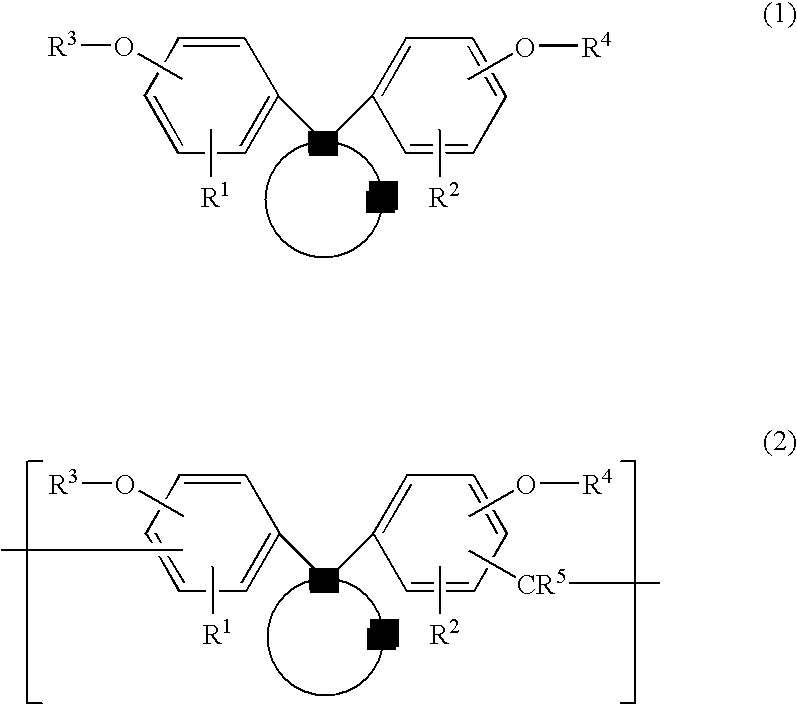
In one aspect, the invention provides a photoresist undercoat-forming material comprising a bisphenol compound having the general formula (1) and a photoresist undercoat-forming material comprising a resin comprising recurring units derived by novolac formation of a bisphenol compound, as represented by the general formula (2).
Figure US07358025-20080415-C00001

Herein R1 and R2 are each independently hydrogen, a straight, branched or cyclic C1-C10 alkyl group, C6-C10 aryl group or C2-C10 alkenyl group. R3 and R4 are each independently hydrogen, a straight, branched or cyclic C1-C6 alkyl group, straight, branched or cyclic C2-C6 alkenyl group, C6-C10 aryl group, C2-C6 acetal group, C2-C6 acyl group or glycidyl group. Z is a divalent C13-C30 hydrocarbon group containing an aromatic skeleton or fused polycyclic hydrocarbon group, which may contain at least one hetero atom. R5 is hydrogen, a straight, branched or cyclic C1-C10 alkyl group or C6-C10 aryl group.
The material may further comprise an organic solvent, a crosslinker and an acid generator.
In another aspect, the invention provides a patterning process comprising the steps of applying the undercoat-forming material defined above onto a processable substrate to form an undercoat layer, applying a photoresist composition onto the undercoat layer to form a photoresist layer, exposing the photoresist layer in a predetermined region to radiation, developing the photoresist layer with a developer to form a photoresist pattern, and processing the undercoat layer and the substrate through the patterned photoresist layer as a mask, by means of a dry etching apparatus. In a preferred embodiment, the photoresist composition comprises a silicon atom-containing polymer, and the processing step includes dry etching the undercoat layer through the photoresist layer as a mask with an oxygen-based etching gas.
In a further aspect, the invention provides a patterning process comprising the steps of applying the undercoat-forming material defined above onto a processable substrate to form an undercoat layer, applying a silicon atom-containing intermediate layer over the undercoat layer, applying a photoresist composition onto the intermediate layer to form a photoresist layer, exposing the photoresist layer in a predetermined region to radiation, developing the photoresist layer with a developer to form a photoresist pattern, processing the intermediate layer through the patterned photoresist layer as a mask, removing the patterned photoresist layer, and processing the undercoat layer and then the substrate through the processed intermediate layer as a mask, the processing steps using a dry etching apparatus. In a preferred embodiment, the photoresist composition comprises a silicon atom-free polymer, and the step of processing the undercoat layer includes dry etching with an oxygen-based etching gas.
BENEFITS OF THE INVENTION
The photoresist undercoat-forming material of the invention, optionally combined with an intermediate layer having an antireflective effect, has an absorptivity coefficient sufficient to provide an antireflective effect at a thickness equal to or more than 200 nm and a high etching resistance as demonstrated by an etching rate with CF4/CHF3 gas and Cl2/BCl3 gas (used in substrate processing) which is slower than conventional m-cresol novolac resins. The resist profile after patterning is satisfactory.
BRIEF DESCRIPTION OF THE DRAWINGS
FIG. 1 is a graph plotting the substrate reflectance versus undercoat layer thickness in bilayer process when the k value of the undercoat layer is fixed at 0.3 and the n value varies from 1.0 to 2.0.
FIG. 2 is a graph plotting the substrate reflectance versus undercoat layer thickness in bilayer process when the n value of the undercoat layer is fixed at 1.5 and the k value varies from 0 to 1.0.
FIG. 3 is a graph plotting the substrate reflectance in trilayer process when the undercoat layer has a fixed n of 1.5, a fixed k of 0.6 and a fixed thickness of 500 nm, and the intermediate layer has a fixed n of 1.5, a k value varying from 0 to 0.4 and a thickness varying from 0 to 400 nm.
FIG. 4 is a graph plotting the substrate reflectance versus varying thickness of the undercoat layer and intermediate layer in trilayer process when the undercoat layer has a fixed n of 1.5 and a fixed k of 0.2, and the intermediate layer has a fixed n of 1.5 and a fixed k of 0.1.
FIG. 5 is a graph plotting the substrate reflectance versus varying thickness of the undercoat layer and intermediate layer in trilayer process when the undercoat layer has a fixed n of 1.5 and a fixed k of 0.6, and the intermediate layer has a fixed n of 1.5 and a fixed k of 0.1.
FIG. 6 illustrates steps of a bilayer resist working process.
FIG. 7 illustrates steps of a trilayer resist working process.
DESCRIPTION OF THE PREFERRED EMBODIMENTS
The notation (Cn-Cm) means a group containing from n to m carbon atoms per group.
The patterning process of the invention involves the steps of applying a photoresist undercoat-forming material comprising a specific bisphenol compound with a group of many carbon atoms as represented by the general formula (1) or a resin comprising recurring units derived by novolac formation of a bisphenol compound as represented by the general formula (2) as a base resin onto a substrate to form an undercoat layer, applying a layer of a photoresist composition over the undercoat layer, optionally with an intermediate layer interposed therebetween, exposing the photoresist layer in a predetermined region to radiation, developing the photoresist layer with a liquid developer to form a resist pattern, and processing the undercoat layer and the substrate through the patterned photoresist layer as a mask, by means of a dry etching apparatus. The undercoat-forming material used herein comprises essentially (A) a specific bisphenol compound with a group of many carbon atoms as represented by the general formula (1) and/or a resin comprising recurring units derived by novolac formation of a bisphenol compound as represented by the general formula (2), and optionally and preferably (B) an organic solvent. For improving the spin coating characteristics, burying of stepped substrates and film's rigidity and solvent resistance, the undercoat-forming material may further comprise (C) a blending polymer, (D) a crosslinker, and (E) an acid generator.
Figure US07358025-20080415-C00002
Herein R1 and R2 are each independently hydrogen, a straight, branched or cyclic C1-C10 alkyl group, C6-C10 aryl group or C2-C10 alkenyl group. R3 and R4 are each independently hydrogen, a straight, branched or cyclic C1-C6 alkyl group, straight, branched or cyclic C2-C6 alkenyl group, C6-C10 aryl group, C2-C6 acetal group, C2-C6 acyl group or glycidyl group. Z is a divalent C13-C30 hydrocarbon group containing an aromatic skeleton or fused polycyclic hydrocarbon group, which may contain at least one hetero atom. R5 is hydrogen, a straight, branched or cyclic C1-C10 alkyl group or C6-C10 aryl group.
Illustrative examples of R1 and R2 include a hydrogen atom, alkyl groups such as methyl, ethyl, propyl, isopropyl, butyl, isobutyl, tert-butyl, pentyl, cyclopentyl, hexyl, cyclohexyl, and octyl, aryl groups such as phenyl, tolyl and xylyl, and alkenyl groups such as vinyl, allyl, propenyl, butenyl, hexenyl and cyclohexenyl. Illustrative examples of R3 and R4 include a hydrogen atom, alkyl, alkenyl and aryl groups as exemplified above, acetal groups such as ethoxyethyl, methoxymethyl, ethoxypropyl, ethoxybutyl, propoxyethyl and butoxyethyl, acyl groups such as acetyl, and glycidyl. Illustrative examples of R5 include a hydrogen atom, alkyl and aryl groups as exemplified above.
Examples of the linking moiety of the formula:
Figure US07358025-20080415-C00003

are illustrated below.
Figure US07358025-20080415-C00004
Figure US07358025-20080415-C00005
Figure US07358025-20080415-C00006
Illustrative, non-limiting examples of the compound having formula (1) are shown below.
Figure US07358025-20080415-C00007
Figure US07358025-20080415-C00008
Figure US07358025-20080415-C00009
Figure US07358025-20080415-C00010
Herein R1, R2, R3 and R4 are as defined above. Preferably R3 and R4 are hydrogen atoms or glycidyl groups, and most preferably hydrogen atoms.
Those compounds of formula (1) wherein R3 and R4 are H may be obtained by reacting a phenol with a corresponding cyclic ketone in a conventional way. Those compounds of formula (1) wherein R3 and R4 are glycidyl groups may be obtained by converting the phenolic hydroxyl group on the phenol into a glycidyl group in a conventional way. Those compounds of formula (1) wherein R3 and R4 are alkyl, alkenyl, aryl, acetal or acyl groups may be similarly obtained by converting the phenolic hydroxyl groups into the desired groups in a conventional way.
On use of the specific bisphenol compound as the undercoat layer according to the invention, the compound of formula (1) itself may be added to form an undercoat layer. Alternatively, the bisphenol compound of formula (1) may be previously converted to a novolac form through condensation reaction with an aldehyde, that is, a resin comprising recurring units of formula (2) may be added.
Examples of the aldehyde which can be used herein include formaldehyde, trioxan, paraformaldehyde, benzaldehyde, acetaldehyde, propylaldehyde, phenylacetaldehyde, α-phenylpropylaldehyde, β-phenylpropylaldehyde, o-hydroxybenzaldehyde, m-hydroxybenzaldehyde, p-hydroxybenzaldehyde, o-chlorobenzaldehyde, m-chlorobenzaldehyde, p-chlorobenzaldehyde, o-nitrobenzaldehyde, m-nitrobenzaldehyde, p-nitrobenzaldehyde, o-methylbenzaldehyde, m-methylbenzaldehyde, p-methylbenzaldehyde, p-ethylbenzaldehyde, p-n-butylbenzaldehyde, and furfural. Inter alia, formaldehyde is most preferred. The aldehydes may be used alone or in admixture. An appropriate amount of the aldehyde used in 0.2 to 5 moles, more preferably 0.5 to 2 moles per mole of the phenol.
Catalysts may be used in the condensation reaction of phenols with aldehydes. Suitable catalysts include acidic catalysts such as hydrochloric acid, nitric acid, sulfuric acid, formic acid, oxalic acid, acetic acid, methanesulfonic acid, camphorsulfonic acid, tosylic acid, and trifluoromethanesulfonic acid. An appropriate amount of the acidic catalyst used is 1×10⁻⁵ to 5×10⁻¹ mole per mole of the phenol.
The aldehyde is not necessarily needed in the event of copolymerization reaction with compounds having an unconjugated double bond such as indene, hydroxyindene, benzofuran, hydroxyanthracene, acenaphthylene, biphenyl, bisphenol, trisphenol, dicyclopentadiene, tetrahydroindene, 4-vinylcyclohexene, norbornadiene, 5-vinylnorborn-2-ene, α-pinene, β-pinene, and limonene.
The polycondensation may be conducted in a reaction medium which is typically water, methanol, ethanol, propanol, butanol, tetrahydrofuran, dioxane or a mixture thereof. The solvent is used in an amount of 0 to 2,000 parts by weight per 100 parts by weight of the reactants.
An appropriate reaction temperature may be selected depending on the reactivity of the reactants, and usually in the range of 10 to 200° C.
The condensation reaction may be conducted by charging the bisphenol, aldehyde and catalyst all at once, or by adding dropwise the bisphenol and aldehyde in the presence of the catalyst.
Once the polycondensation reaction is completed, the unreacted reactants, catalyst and the like may be removed from the system by elevating the temperature of the reactor vessel to 130 to 230° C. for evaporating off the volatiles at about 1 to 50 mmHg.
The bisphenol of formula (1) may be polymerized alone or copolymerized with another phenol.
Examples of the phenol which can be copolymerized include phenol, o-cresol, m-cresol, p-cresol, 2,3-dimethylphenol, 2,5-dimethylphenol, 3,4-dimethylphenol, 3,5-dimethylphenol, 2,4-dimethylphenol, 2,6-dimethylphenol, 2,3,5-trimethylphenol, 3,4,5-trimethylphenol, 2-t-butylphenol, 3-t-butylphenol, 4-t-butylphenol, 2-phenylphenol, 3-phenylphenol, 4-phenylphenol, 3,5-diphenylphenol, 2-naphthylphenol, 3-naphthylphenol, 4-naphthylphenol, 4-tritylphenol, resorcinol, 2-methylresorcinol, 4-methylresorcinol, 5-methylresorcinol, catechol, 4-t-butylcatechol, 2-methoxyphenol, 3-methoxyphenol, 2-propylphenol, 3-propylphenol, 4-propylphenol, 2-isopropylphenol, 3-isopropylphenol, 4-isopropylphenol, 2-methoxy-5-methylphenol, 2-t-butyl-5-methylphenol, pyrogallol, thymol, and isothymol.
Besides, any copolymerizable monomers may be further copolymerized. Examples of suitable monomers include 1-naphthol, 2-naphthol, 2-methyl-1-naphthol, 4-methoxy-1-naphthol, 7-methoxy-2-naphthol and dihydroxynaphthalenes such as 1,5-dihydroxynaphthalene, 1,7-dihydroxynaphthalene, and 2,6-dihydroxynaphthalene; methyl 3-hydroxy-naphthalene-2-carboxylate, indene, hydroxyindene, benzofuran, hydroxyanthracene, acenaphthylene, biphenyl, bisphenol, trisphenol, dicyclopentadiene, tetrahydroindene, 4-vinylcyclohexene, norbornadiene, 5-vinylnorborn-2-ene, α-pinene, β-pinene, and limonene. Copolymers of three or more components including any of these monomers are acceptable.
The novolac resin thus obtained should preferably include 10 to 100 mol %, more preferably 30 to 100 mol % of the recurring units of formula (2). The content of recurring units derived from the copolymerizable phenol is preferably 0 to 90 mol %, more preferably 0 to 70 mol %, and the content of recurring units derived from the copolymerizable monomer is preferably 0 to 90 mol %, more preferably 0 to 70 mol %.
The novolac resin should preferably have a weight average molecular weight (Mw) in the range of about 1,000 to about 30,000, more preferably about 2,000 to about 20,000, as measured by gel permeation chromatography (GPC) versus polystyrene standards. Their molecular weight distribution or dispersity (Mw/Mn) is preferably in the range of 1.2 to 7. A narrow dispersity which is arrived at by cutting off monomer components, oligomeric components or low molecular weight components having a Mw of not more than 1,000 offers benefits of more efficient crosslinking and reduced amounts of volatile components during baking, preventing contamination around the baking cup.
Into the novolac resin after condensation, a fused aromatic or alicyclic substituent group may be subsequently introduced at the ortho-position relative to phenol, using an acidic catalyst.
Illustrative examples of the substituent group which can be introduced are given below.
Figure US07358025-20080415-C00011
Figure US07358025-20080415-C00012
Figure US07358025-20080415-C00013
Of these substituent groups, polycyclic aromatic groups such as anthracenemethyl and pyrenemethyl groups are most preferred for 248-nm exposure. Those groups having alicyclic and naphthalene structures are preferred for improved transparency at 193 nm. In contrast, since the benzene ring has a window of improved transparency at the wavelength 157 nm, the absorption wavelength must be shifted so as to increase the absorption. The furan ring has absorption at a shorter wavelength than the benzene ring and is thus improved in absorption at 157 nm, but to a very small extent. Naphthalene, anthracene and pyrene rings are preferably used because of increased absorption due to a shift of the absorption wavelength to longer side and because these aromatic rings have the additional advantage of improved etching resistance.
The method of introducing a substituent group is by adding an alcohol whose hydroxyl group provides an attachment site of the substituent group to the polymer as polymerized in the presence of an acid catalyst, for thereby introducing the substituent group at the ortho- or para-position relative to the hydroxy group on the phenol. Suitable acid catalysts include acidic catalysts such as hydrochloric acid, nitric acid, sulfuric acid, formic acid, oxalic acid, acetic acid, methanesulfonic acid, n-butanesulfonic acid, camphorsulfonic acid, tosylic acid, and trifluoromethanesulfonic acid. An appropriate amount of the acidic catalyst used is 1×10⁻⁵ to 5×10⁻¹ mole per mole of the phenol. An appropriate amount of the substituent group introduced is in the range of 0 to 0.8 mole per mole of hydroxyl group on the phenol.
The inventive resin comprising recurring units of formula (2) can be hydrogenated to further improve its transparency at 193 nm. The degree of hydrogenation is preferably up to 80 mol %, more preferably up to 60 mol % of the aromatic groups.
Further, the inventive resin can be blended with another polymer. Preferred for this blending purpose are polymers which can serve the functions of improving film formation by spin coating and burying in stepped substrates when mixed with the compound of formula (1) or the novolac resin comprising recurring units of formula (2). More preferably a choice may be made of materials having a high carbon density and etching resistance. Suitable materials include novolac resins derived from phenol, o-cresol, m-cresol, p-cresol, 2,3-dimethylphenol, 2,5-dimethylphenol, 3,4-dimethylphenol, 3,5-dimethylphenol, 2,4-dimethylphenol, 2,6-dimethylphenol, 2,3,5-trimethylphenol, 3,4,5-trimethylphenol, 2-t-butylphenol, 3-t-butylphenol, 4-t-butylphenol, 2-phenylphenol, 3-phenylphenol, 4-phenylphenol, 3,5-diphenylphenol, 2-naphthylphenol, 3-naphthylphenol, 4-naphthylphenol, 4-tritylphenol, resorcinol, 2-methylresorcinol, 4-methylresorcinol, 5-methylresorcinol, catechol, 4-t-butylcatechol, 2-methoxyphenol, 3-methoxyphenol, 2-propylphenol, 3-propylphenol, 4-propylphenol, 2-isopropylphenol, 3-isopropylphenol, 4-isopropylphenol, 2-methoxy-5-methylphenol, 2-t-butyl-5-methylphenol, pyrogallol, thymol, isothymol, 4,4′-(9H-fluoren-9-ylidene)bisphenol, 2,2′-dimethyl-4,4′-(9H-fluoren-9-ylidene)bisphenol, 2,2′-diallyl-4,4′-(9H-fluoren-9-ylidene)bisphenol, 2,2′-difluoro-4,4′-(9H-fluoren-9-ylidene)bisphenol, 2,2′-diphenyl-4,4′-(9H-fluoren-9-ylidene)bisphenol, 2,2′-dimethoxy-4,4′-(9H-fluoren-9-ylidene)bisphenol, 2,3,2′,3′-tetrahydro-(1,1′)-spirobiindene-6,6′-diol, 3,3,3′,3′-tetramethyl-2,3,2′,3′-tetrahydro-(1,1′)-spirobiindene-6,6′-diol, 3,3,3′,3′,4,4′-hexamethyl-2,3,2′,3′-tetrahydro-(1,1′)-spirobiindene-6,6′-diol, 2,3,2′,3′-tetrahydro-(1,1′)-spirobiindene-5,5′-diol, 5,5′-dimethyl-3,3,3′,3′-tetramethyl-2,3,2′,3′-tetrahydro-(1,1′)-spirobiindene-6,6′-diol, 1-naphthol, 2-naphthol, 2-methyl-1-naphthol, 4-methoxy-1-naphthol, 7-methoxy-2-naphthol, and dihydroxynaphthalenes such as 1,5-dihydroxynaphthalene, 1,7-dihydroxynaphthalene and 2,6-dihydroxynaphthalene, methyl 3-hydroxy-naphthalene-2-carboxylate, indene, hydroxyindene, benzofuran, hydroxyanthracene, acenaphthylene, biphenyl, bisphenol, trisphenol, dicyclopentadiene, tetrahydroindene, 4-vinylcyclohexene, norbornadiene, 5-vinylnorborn-2-ene, α-pinene, β-pinene, limonene, etc.; and polyhydroxystyrene, polystyrene, polyvinyl naphthalene, polyvinyl anthracene, polyvinyl carbazole, polyindene, polyacenaphthylene, polynorbornene, polycyclodecene, polytetracyclododecene, polynortricyclene, poly(meth)acrylate, and copolymers thereof.
The amount of the blending polymer compounded is usually 0 to 1,000 parts by weight, preferably 0 to 500 parts by weight per 100 parts by weight of the compound of formula (1) or the resin of formula (2).
One of the functions required for the undercoat layer including an antireflective film is the elimination of intermixing with the overcoat layer (i.e., silicon-containing intermediate layer and resist layer) and the elimination of diffusion of low molecular weight components into the overcoat layer (see Proc. SPIE Vol. 2195, pp. 225-229 (1994)). One common means for preventing intermixing and diffusion is by baking an antireflective film as spin coated for inducing thermal crosslinkage. Then, in the event the antireflective film material contains a crosslinker, a method of introducing crosslinkable substituent groups into the polymer may be employed. Absent a particular crosslinker, the specific bisphenol compound with a group of many carbon atoms represented by formula (1) and a novolac resin comprising recurring units derived by novolac formation of a bisphenol compound, as represented by the general formula (2) can be crosslinked by heating at a temperature of 300° C. or higher for inducing condensation reaction of hydroxyl groups.
Crosslinker
Examples of the crosslinker which can be used herein include melamine compounds, guanamine compounds, glycoluril compounds and urea compounds having substituted thereon at least one group selected from among methylol, alkoxymethyl and acyloxymethyl groups, epoxy compounds, thioepoxy compounds, isocyanate compounds, azide compounds, and compounds having a double bond such as an alkenyl ether group. These compounds may be used as an additive or introduced as pendant groups on polymer side chains. Compounds having a hydroxy group are also useful as the crosslinker.
Of the foregoing compounds, examples of suitable epoxy compounds include tris(2,3-epoxypropyl)isocyanurate, trimethylolmethane triglycidyl ether, trimethylolpropane triglycidyl ether, and triethylolethane triglycidyl ether. Examples of the melamine compound include hexamethylol melamine, hexamethoxymethyl melamine, hexamethylol melamine compounds having 1 to 6 methylol groups methoxymethylated and mixtures thereof, hexamethoxyethyl melamine, hexaacyloxymethyl melamine, hexamethylol melamine compounds having 1 to 6 methylol groups acyloxymethylated and mixtures thereof. Examples of the guanamine compound include tetramethylol guanamine, tetramethoxymethyl guanamine, tetramethylol guanamine compounds having 1 to 4 methylol groups methoxymethylated and mixtures thereof, tetramethoxyethyl guanamine, tetraacyloxyguanamine, tetramethylol guanamine compounds having 1 to 4 methylol groups acyloxymethylated and mixtures thereof. Examples of the glycoluril compound include tetramethylol glycoluril, tetramethoxyglycoluril, tetramethoxymethyl glycoluril, tetramethylol glycoluril compounds having 1 to 4 methylol groups methoxymethylated and mixtures thereof, tetramethylol glycoluril compounds having 1 to 4 methylol groups acyloxymethylated and mixtures thereof. Examples of the urea compound include tetramethylol urea, tetramethoxymethyl urea, tetramethylol urea compounds having 1 to 4 methylol groups methoxymethylated and mixtures thereof, and tetramethoxyethyl urea.
Examples of the alkenyl ether group-containing compound include ethylene glycol divinyl ether, triethylene glycol divinyl ether, 1,2-propanediol divinyl ether, 1,4-butanediol divinyl ether, tetramethylene glycol divinyl ether, neopentyl glycol divinyl ether, trimethylol propane trivinyl ether, hexanediol divinyl ether, 1,4-cyclohexanediol divinyl ether, pentaerythritol trivinyl ether, pentaerythritol tetravinyl ether, sorbitol tetravinyl ether, sorbitol pentavinyl ether, and trimethylol propane trivinyl ether.
Also useful as the crosslinker are alcoholic group-containing compounds and low-nuclear phenol compounds whose hydroxyl group is converted to a glycidyl ether form using epichlorohydrin. Suitable alcoholic group-containing compounds include naphthol novolac, m- and p-cresol novolac, naphthol-dicyclopentadiene novolac, m- and p-cresol-dicyclopentadiene novolac, 4,8-bis(hydroxymethyl)tricyclo[5.2.1.02,6]-decane, pentaerythritol, 1,2,6-hexanetriol, 4,4′,4″-methylidene triscyclohexanol, 4,4′-[1-[4-[1-(4-hydroxycyclohexyl)-1-methylethyl]phenyl]-ethylidene]biscyclohexanol, [1,1′-bicyclohexyl]-4,4′-diol, methylenebiscyclohexanol, decahydronaphthalene-2,6-diol, and [1,1′-bicyclohexyl]-3,3′,4,4′-tetrahydroxy. Suitable low-nuclear phenol compounds include bisphenol, methylene bisphenol, 2,2′-methylenebis[4-methylphenol], 4,4′-methylidene-bis[2,6-dimethylphenol], 4,4′-(1-methyl-ethylidene)bis[2-methylphenol], 4,4′-cyclohexylidene bisphenol, 4,4′-(1,3-dimethylbutylidene)bisphenol, 4,4′-(1-methylethylidene)bis[2,6-dimethylphenol], 4,4′-oxybisphenol, 4,4′-methylenebisphenol, bis(4-hydroxyphenyl)methanone, 4,4′-methylene bis[2-methylphenol], 4,4′-[1,4-phenylenebis(1-methylethylidene)]bisphenol, 4,4′-(1,2-ethanediyl)bisphenol, 4,4′-(diethylsilylene)bisphenol, 4,4′-[2,2,2-trifluoro-1-(trifluoromethyl)ethylidene]-bisphenol, 4,4′,4″-methylidene trisphenol, 4,4′-[1-(4-hydroxyphenyl)-1-methylethyl]phenyl]ethylidene]-bisphenol, 2,6-bis[(2-hydroxy-5-methylphenyl)methyl]-4-methylphenol, 4,4′,4″-ethylidyne tris[2-methylphenol], 4,4′,4″-ethylidyne trisphenol, 4,6-bis[(4-hydroxyphenyl)methyl]-1,3-benzenediol, 4,4′-[(3,4-dihydroxyphenyl)methylene]bis[2-methylphenol], 4,4′,4″,4′″-(1,2-ethanediylidene)tetrakisphenol, 4,4′,4″,4′″-(1,2-ethanediylidene)tetrakis[2-methylphenol], 2,2′-methylenebis[6-[(2-hydroxy-5-methylphenyl)methyl]-4-methylphenol], 4,4′,4″,4′″-(1,4-phenylenedimethylidyne)tetrakisphenol, 2,4,6-tris(4-hydroxyphenylmethyl)-1,3-benzenediol, 2,4′,4″-methylidenetrisphenol, 4,4′,4′″-(3-methyl-1-propanyl-3-ylidene)trisphenol, 2,6-bis[(4-hydroxy-3-fluorophenyl)methyl]-4-fluorophenol, 2,6-bis[4-hydroxy-3-fluorophenyl]methyl]-4-fluorophenol, 3,6-bis[(3,5-dimethyl-4-hydroxyphenyl)methyl]-1,2-benzenediol, 4,6-bis[(3,5-dimethyl-4-hydroxyphenyl)methyl]-1,3-benzenediol, p-methylcalix[4]arene, 2,2′-methylenebis[6-[(2,5/3,6-dimethyl-4/2-hydroxyphenyl)-methyl]-4-methylphenol, 2,2′-methylenebis[6-[(3,5-dimethyl-4-hydroxyphenyl)methyl]-4-methylphenol, 4,4′,4″,4′″-tetrakis[(1-methylethylidene)bis(1,4-cyclohexylidene)]phenol, 6,6′-methylenebis[4-(4-hydroxyphenylmethyl)-1,2,3-benzenetriol, and 3,3′,5,5′-tetrakis[(5-methyl-2-hydroxyphenyl)methyl]-[(1,1′-biphenyl)-4,4′-diol].
In the inventive undercoat-forming material, the crosslinker is preferably compounded in an amount of 3 to 50 parts by weight, more preferably 5 to 40 parts by weight per 100 parts by weight of the total of the compound of formula (1), the resin comprising recurring units of formula (2) and the blending polymer (the total being referred to as “base polymer,” hereinafter). Less than 3 pbw of the crosslinker may allow for mixing with the resist. More than 50 pbw of the crosslinker may invite a degraded antireflection effect, cracking of the crosslinked film or a lowering of etching resistance due to a drop of carbon density.
Acid Generator
In the practice of the invention, an acid generator may be added to accelerate the thermally induced crosslinking reaction. Acid generators include those which generate an acid through pyrolysis and those which generate an acid upon exposure to light, and both are useful.
The acid generators used herein include
  • (i) onium salts of the formula (P1a-1), (P1a-2), (P1a-3) or (P1b),
  • (ii) diazomethane derivatives of the formula (P2),
  • (iii) glyoxime derivatives of the formula (P3),
  • (iv) bissulfone derivatives of the formula (P4),
  • (v) sulfonic acid esters of N-hydroxyimide compounds of the formula (P5),
  • (vi) β-ketosulfonic acid derivatives,
  • (vii) disulfone derivatives,
  • (viii) nitrobenzylsulfonate derivatives, and
  • (ix) sulfonate derivatives.
These acid generators are described in detail.
(i) Onium Salts of Formula (P1a-1), (P1a-2) or (P1a-3):
Figure US07358025-20080415-C00014
Herein, R101a, R101b, and R101c independently represent straight, branched or cyclic alkyl, alkenyl, oxoalkyl or oxoalkenyl groups of 1 to 12 carbon atoms, aryl groups of 6 to 20 carbon atoms, or aralkyl or aryloxoalkyl groups of 7 to 12 carbon atoms, wherein some or all of the hydrogen atoms may be replaced by alkoxy or other groups. Also, R101b and R101c, taken together, may form a ring. R101b and R101c each are alkylene groups of 1 to 6 carbon atoms when they form a ring. K is a non-nucleophilic counter ion. R101d, R101e, R101f, and R101g stand for the same as R101a, R101b, and R101c as well as hydrogen atoms. A pair of R101d and R101e or a combination of R101d, R101e and R101f may form a ring, and each of R101d and R101e or each of R101d, R101e and R101f is an alkylene group of 3 to 10 carbon atoms when they form a ring. R101d, R101e, R101f, and R101g, taken together, may stand for a heterocyclic aromatic ring having the nitrogen atom (in the formula) incorporated therein.
R101a, R101b, R101c, R101d, R101e, R101f, and R101g may be the same or different and are illustrated below. Exemplary alkyl groups include methyl, ethyl, propyl, isopropyl, n-butyl, sec-butyl, tert-butyl, pentyl, hexyl, heptyl, octyl, cyclopentyl, cyclohexyl, cycloheptyl, cyclopropylmethyl, 4-methylcyclohexyl, cyclohexylmethyl, norbornyl, and adamantyl. Exemplary alkenyl groups include vinyl, allyl, propenyl, butenyl, hexenyl, and cyclohexenyl. Exemplary oxoalkyl groups include 2-oxocyclopentyl and 2-oxocyclohexyl as well as 2-oxopropyl, 2-cyclopentyl-2-oxoethyl, 2-cyclohexyl-2-oxoethyl, and 2-(4-methylcyclohexyl)-2-oxoethyl. Exemplary aryl groups include phenyl and naphthyl; alkoxyphenyl groups such as p-methoxyphenyl, m-methoxyphenyl, o-methoxyphenyl, ethoxyphenyl, p-tert-butoxyphenyl, and m-tert-butoxyphenyl; alkylphenyl groups such as 2-methylphenyl, 3-methylphenyl, 4-methylphenyl, ethylphenyl, 4-tert-butylphenyl, 4-butylphenyl, and dimethylphenyl; alkylnaphthyl groups such as methylnaphthyl and ethylnaphthyl; alkoxynaphthyl groups such as methoxynaphthyl and ethoxynaphthyl; dialkylnaphthyl groups such as dimethylnaphthyl and diethylnaphthyl; and dialkoxynaphthyl groups such as dimethoxynaphthyl and diethoxynaphthyl. Exemplary aralkyl groups include benzyl, phenylethyl, and phenethyl. Exemplary aryloxoalkyl groups are 2-aryl-2-oxoethyl groups such as 2-phenyl-2-oxoethyl, 2-(1-naphthyl)-2-oxoethyl, and 2-(2-naphthyl)-2-oxoethyl. Examples of the non-nucleophilic counter ion represented by K include halide ions such as chloride and bromide ions, fluoroalkylsulfonate ions such as triflate, 1,1,1-trifluoroethanesulfonate, and nonafluorobutanesulfonate, arylsulfonate ions such as tosylate, benzenesulfonate, 4-fluorobenzenesulfonate, and 1,2,3,4,5-pentafluorobenzenesulfonate, and alkylsulfonate ions such as mesylate and butanesulfonate.
Examples of the heterocyclic aromatic ring having the nitrogen atom (in formula (P1a-3)) incorporated therein, represented by R101d, R101e, R101f, and R101g include imidazole derivatives (e.g., imidazole, 4-methylimidazole, and 4-methyl-2-phenylimidazole), pyrazole derivatives, furazan derivatives, pyrroline derivatives (e.g., pyrroline and 2-methyl-1-pyrroline), pyrrolidine derivatives (e.g., pyrrolidine, N-methylpyrrolidine, pyrrolidinone, and N-methylpyrrolidone), imidazoline derivatives, imidazolidine derivatives, pyridine derivatives (e.g., pyridine, methylpyridine, ethylpyridine, propylpyridine, butylpyridine, 4-(1-butylpentyl)pyridine, dimethylpyridine, trimethylpyridine, triethylpyridine, phenylpyridine, 3-methyl-2-phenylpyridine, 4-tert-butylpyridine, diphenylpyridine, benzylpyridine, methoxypyridine, butoxypyridine, dimethoxypyridine, 1-methyl-2-pyridone, 4-pyrrolidinopyridine, 1-methyl-4-phenylpyridine, 2-(1-ethylpropyl)pyridine, aminopyridine, and dimethylaminopyridine), pyridazine derivatives, pyrimidine derivatives, pyrazine derivatives, pyrazoline derivatives, pyrazolidine derivatives, piperidine derivatives, piperazine derivatives, morpholine derivatives, indole derivatives, isoindole derivatives, 1H-indazole derivatives, indoline derivatives, quinoline derivatives (e.g., quinoline and 3-quinolinecarbonitrile), isoquinoline derivatives, cinnoline derivatives, quinazoline derivatives, quinoxaline derivatives, phthalazine derivatives, purine derivatives, pteridine derivatives, carbazole derivatives, phenanthridine derivatives, acridine derivatives, phenazine derivatives, 1,10-phenanthroline derivatives, adenine derivatives, adenosine derivatives, guanine derivatives, guanosine derivatives, uracil derivatives, and uridine derivatives.
The salts of (P1a-1) and (P1a-2) have both the functions of a photoacid generator and a thermal acid generator while the salts of (P1a-3) function as a thermal acid generator.
Figure US07358025-20080415-C00015
Herein, R102a and R102b independently represent straight, branched or cyclic alkyl groups of 1 to 8 carbon atoms. R103 represents a straight, branched or cyclic alkylene group of 1 to 10 carbon atoms. R104a and R104b independently represent 2-oxoalkyl groups of 3 to 7 carbon atoms. K is a non-nucleophilic counter ion.
Illustrative of the groups represented by R102a and R102b are methyl, ethyl, propyl, isopropyl, n-butyl, sec-butyl, tert-butyl, pentyl, hexyl, heptyl, octyl, cyclopentyl, cyclohexyl, cyclopropylmethyl, 4-methylcyclohexyl, and cyclohexylmethyl. Illustrative of the groups represented by R103 are methylene, ethylene, propylene, butylene, pentylene, hexylene, heptylene, octylene, nonylene, 1,4-cyclohexylene, 1,2-cyclohexylene, 1,3-cyclopentylene, 1,4-cyclooctylene, and 1,4-cyclohexanedimethylene. Illustrative of the groups represented by R104a and R104b are 2-oxopropyl, 2-oxocyclopentyl, 2-oxocyclohexyl, and 2-oxocycloheptyl. Illustrative examples of the counter ion represented by K are the same as exemplified for formulae (P1a-1), (P1a-2) and (P1a-3).
(ii) Diazomethane Derivatives of Formula (P2)
Figure US07358025-20080415-C00016
Herein, R105 and R106 independently represent straight, branched or cyclic alkyl or halogenated alkyl groups of 1 to 12 carbon atoms, aryl or halogenated aryl groups of 6 to 20 carbon atoms, or aralkyl groups of 7 to 12 carbon atoms.
Of the groups represented by R105 and R106, exemplary alkyl groups include methyl, ethyl, propyl, isopropyl, n-butyl, sec-butyl, tert-butyl, pentyl, hexyl, heptyl, octyl, amyl, cyclopentyl, cyclohexyl, cycloheptyl, norbornyl, and adamantyl. Exemplary halogenated alkyl groups include trifluoromethyl, 1,1,1-trifluoroethyl, 1,1,1-trichloroethyl, and nonafluorobutyl. Exemplary aryl groups include phenyl; alkoxyphenyl groups such as p-methoxyphenyl, m-methoxyphenyl, o-methoxyphenyl, ethoxyphenyl, p-tert-butoxyphenyl, and m-tert-butoxyphenyl; and alkylphenyl groups such as 2-methylphenyl, 3-methylphenyl, 4-methylphenyl, ethylphenyl, 4-tert-butylphenyl, 4-butylphenyl, and dimethylphenyl. Exemplary halogenated aryl groups include fluorophenyl, chlorophenyl, and 1,2,3,4,5-pentafluorophenyl. Exemplary aralkyl groups include benzyl and phenethyl.
(iii) Glyoxime Derivatives of Formula (P3)
Figure US07358025-20080415-C00017
Herein R107, R108, and R109 independently represent straight, branched or cyclic alkyl or halogenated alkyl groups of 1 to 12 carbon atoms, aryl or halogenated aryl groups of 6 to 20 carbon atoms, or aralkyl groups of 7 to 12 carbon atoms. Also, R108 and R109, taken together, may form a ring. R108 and R109 each are straight or branched alkylene groups of 1 to 6 carbon atoms when they form a ring.
Illustrative examples of the alkyl, halogenated alkyl, aryl, halogenated aryl, and aralkyl groups represented by R107, R108, and R109 are the same as exemplified for R105 and R106. Examples of the alkylene groups represented by R108 and R109 include methylene, ethylene, propylene, butylene, and hexylene.
(iv) Bissulfone Derivatives of Formula (P4)
Figure US07358025-20080415-C00018
Herein, R101a and R101b are as defined above.
(v) Sulfonic Acid Esters of N-Hydroxyimide Compounds of Formula (P5)
Figure US07358025-20080415-C00019

Herein, R110 is an arylene group of 6 to 10 carbon atoms, alkylene group of 1 to 6 carbon atoms, or alkenylene group of 2 to 6 carbon atoms wherein some or all of the hydrogen atoms may be replaced by straight or branched alkyl or alkoxy groups of 1 to 4 carbon atoms, nitro, acetyl, or phenyl groups. R111 is a straight, branched or cyclic alkyl group of 1 to 8 carbon atoms, alkenyl, alkoxyalkyl, phenyl or naphthyl group wherein some or all of the hydrogen atoms may be replaced by alkyl or alkoxy groups of 1 to 4 carbon atoms, phenyl groups (which may have substituted thereon an alkyl or alkoxy of 1 to 4 carbon atoms, nitro, or acetyl group), hetero-aromatic groups of 3 to 5 carbon atoms, or chlorine or fluorine atoms.
Of the groups represented by R110, exemplary arylene groups include 1,2-phenylene and 1,8-naphthylene; exemplary alkylene groups include methylene, ethylene, trimethylene, tetramethylene, phenylethylene, and norbornane-2,3-diyl; and exemplary alkenylene groups include 1,2-vinylene, 1-phenyl-1,2-vinylene, and 5-norbornene-2,3-diyl. Of the groups represented by R111, exemplary alkyl groups are as exemplified for R101a to R101c; exemplary alkenyl groups include vinyl, 1-propenyl, allyl, 1-butenyl, 3-butenyl, isoprenyl, 1-pentenyl, 3-pentenyl, 4-pentenyl, dimethylallyl, 1-hexenyl, 3-hexenyl, 5-hexenyl, 1-heptenyl, 3-heptenyl, 6-heptenyl, and 7-octenyl; and exemplary alkoxyalkyl groups include methoxymethyl, ethoxymethyl, propoxymethyl, butoxymethyl, pentyloxymethyl, hexyloxymethyl, heptyloxymethyl, methoxyethyl, ethoxyethyl, propoxyethyl, butoxyethyl, pentyloxyethyl, hexyloxyethyl, methoxypropyl, ethoxypropyl, propoxypropyl, butoxypropyl, methoxybutyl, ethoxybutyl, propoxybutyl, methoxypentyl, ethoxypentyl, methoxyhexyl, and methoxyheptyl.
Of the substituents on these groups, the alkyl groups of 1 to 4 carbon atoms include methyl, ethyl, propyl, isopropyl, n-butyl, isobutyl and tert-butyl; the alkoxy groups of 1 to 4 carbon atoms include methoxy, ethoxy, propoxy, isopropoxy, n-butoxy, isobutoxy, and tert-butoxy; the phenyl groups which may have substituted thereon an alkyl or alkoxy of 1 to 4 carbon atoms, nitro, or acetyl group include phenyl, tolyl, p-tert-butoxyphenyl, p-acetylphenyl and p-nitrophenyl; the hetero-aromatic groups of 3 to 5 carbon atoms include pyridyl and furyl.
Illustrative examples of the acid generator include:
onium salts such as
  • tetramethylammonium trifluoromethanesulfonate,
  • tetramethylammonium nonafluorobutanesulfonate,
  • triethylammonium nonafluorobutanesulfonate,
  • pyridinium nonafluorobutanesulfonate,
  • triethylammonium camphorsulfonate,
  • pyridinium camphorsulfonate,
  • tetra-n-butylammonium nonafluorobutanesulfonate,
  • tetraphenylammonium nonafluorobutanesulfonate,
  • tetramethylammonium p-toluenesulfonate,
  • diphenyliodonium trifluoromethanesulfonate,
  • (p-tert-butoxyphenyl)phenyliodonium trifluoromethanesulfonate,
  • diphenyliodonium p-toluenesulfonate,
  • (p-tert-butoxyphenyl)phenyliodonium p-toluenesulfonate,
  • triphenylsulfonium trifluoromethanesulfonate,
  • (p-tert-butoxyphenyl)diphenylsulfonium trifluoromethanesulfonate,
  • bis(p-tert-butoxyphenyl)phenylsulfonium trifluoromethane-sulfonate,
  • tris(p-tert-butoxyphenyl)sulfonium trifluoromethanesulfonate,
  • triphenylsulfonium p-toluenesulfonate,
  • (p-tert-butoxyphenyl)diphenylsulfonium p-toluenesulfonate,
  • bis(p-tert-butoxyphenyl)phenylsulfonium p-toluenesulfonate,
  • tris(p-tert-butoxyphenyl)sulfonium p-toluenesulfonate,
  • triphenylsulfonium nonafluorobutanesulfonate,
  • triphenylsulfonium butanesulfonate,
  • trimethylsulfonium trifluoromethanesulfonate,
  • trimethylsulfonium p-toluenesulfonate,
  • cyclohexylmethyl(2-oxocyclohexyl)sulfonium trifluoromethane-sulfonate,
  • cyclohexylmethyl(2-oxocyclohexyl)sulfonium p-toluenesulfonate,
  • dimethylphenylsulfonium trifluoromethanesulfonate,
  • dimethylphenylsulfonium p-toluenesulfonate,
  • dicyclohexylphenylsulfonium trifluoromethanesulfonate,
  • dicyclohexylphenylsulfonium p-toluenesulfonate,
  • trinaphthylsulfonium trifluoromethanesulfonate,
  • cyclohexylmethyl(2-oxocyclohexyl)sulfonium trifluoromethane-sulfonate,
  • (2-norbornyl)methyl(2-oxocyclohexyl)sulfonium trifluoromethanesulfonate,
  • ethylenebis[methyl(2-oxocyclopentyl)sulfonium trifluoromethanesulfonate], and
  • 1,2′-naphthylcarbonylmethyltetrahydrothiophenium triflate;
diazomethane derivatives such as
  • bis(benzenesulfonyl)diazomethane,
  • bis(p-toluenesulfonyl)diazomethane,
  • bis(xylenesulfonyl)diazomethane,
  • bis(cyclohexylsulfonyl)diazomethane,
  • bis(cyclopentylsulfonyl)diazomethane,
  • bis(n-butylsulfonyl)diazomethane,
  • bis(isobutylsulfonyl)diazomethane,
  • bis(sec-butylsulfonyl)diazomethane,
  • bis(n-propylsulfonyl)diazomethane,
  • bis(isopropylsulfonyl)diazomethane,
  • bis(tert-butylsulfonyl)diazomethane,
  • bis(n-amylsulfonyl)diazomethane,
  • bis(isoamylsulfonyl)diazomethane,
  • bis(sec-amylsulfonyl)diazomethane,
  • bis(tert-amylsulfonyl)diazomethane,
  • 1-cyclohexylsulfonyl-1-(tert-butylsulfonyl)diazomethane,
  • 1-cyclohexylsulfonyl-1-(tert-amylsulfonyl)diazomethane, and
  • 1-tert-amylsulfonyl-1-(tert-butylsulfonyl)diazomethane;
glyoxime derivatives such as
  • bis-O-(p-toluenesulfonyl)-α-dimethylglyoxime,
  • bis-O-(p-toluenesulfonyl)-α-diphenylglyoxime,
  • bis-O-(p-toluenesulfonyl)-α-dicyclohexylglyoxime,
  • bis-O-(p-toluenesulfonyl)-2,3-pentanedioneglyoxime,
  • bis-O-(p-toluenesulfonyl)-2-methyl-3,4-pentanedioneglyoxime,
  • bis-O-(n-butanesulfonyl)-α-dimethylglyoxime,
  • bis-O-(n-butanesulfonyl)-α-diphenylglyoxime,
  • bis-O-(n-butanesulfonyl)-α-dicyclohexylglyoxime,
  • bis-O-(n-butanesulfonyl)-2,3-pentanedioneglyoxime,
  • bis-O-(n-butanesulfonyl)-2-methyl-3,4-pentanedioneglyoxime,
  • bis-O-(methanesulfonyl)-α-dimethylglyoxime,
  • bis-O-(trifluoromethanesulfonyl)-α-dimethylglyoxime,
  • bis-O-(1,1,1-trifluoroethanesulfonyl)-α-dimethylglyoxime,
  • bis-O-(tert-butanesulfonyl)-α-dimethylglyoxime,
  • bis-O-(perfluorooctanesulfonyl)-α-dimethylglyoxime,
  • bis-O-(cyclohexanesulfonyl)-α-dimethylglyoxime,
  • bis-O-(benzenesulfonyl)-α-dimethylglyoxime,
  • bis-O-(p-fluorobenzenesulfonyl)-α-dimethylglyoxime,
  • bis-O-(p-tert-butylbenzenesulfonyl)-α-dimethylglyoxime,
  • bis-O-(xylenesulfonyl)-α-dimethylglyoxime, and
  • bis-O-(camphorsulfonyl)-α-dimethylglyoxime;
bissulfone derivatives such as
  • bisnaphthylsulfonylmethane, bistrifluoromethylsulfonylmethane,
  • bismethylsulfonylmethane, bisethylsulfonylmethane,
  • bispropylsulfonylmethane, bisisopropylsulfonylmethane,
  • bis-p-toluenesulfonylmethane, and bisbenzenesulfonylmethane;
β-ketosulfone derivatives such as
  • 2-cyclohexylcarbonyl-2-(p-toluenesulfonyl)propane and
  • 2-isopropylcarbonyl-2-(p-toluenesulfonyl)propane;
disulfone derivatives such as diphenyl disulfone derivatives and dicyclohexyl disulfone derivatives;
nitrobenzyl sulfonate derivatives such as
  • 2,6-dinitrobenzyl p-toluenesulfonate and
  • 2,4-dinitrobenzyl p-toluenesulfonate;
sulfonic acid ester derivatives such as
  • 1,2,3-tris(methanesulfonyloxy)benzene,
  • 1,2,3-tris(trifluoromethanesulfonyloxy)benzene, and
  • 1,2,3-tris(p-toluenesulfonyloxy)benzene; and
sulfonic acid esters of N-hydroxyimides such as
  • N-hydroxysuccinimide methanesulfonate,
  • N-hydroxysuccinimide trifluoromethanesulfonate,
  • N-hydroxysuccinimide ethanesulfonate,
  • N-hydroxysuccinimide 1-propanesulfonate,
  • N-hydroxysuccinimide 2-propanesulfonate,
  • N-hydroxysuccinimide 1-pentanesulfonate,
  • N-hydroxysuccinimide 1-octanesulfonate,
  • N-hydroxysuccinimide p-toluenesulfonate,
  • N-hydroxysuccinimide p-methoxybenzenesulfonate,
  • N-hydroxysuccinimide 2-chloroethanesulfonate,
  • N-hydroxysuccinimide benzenesulfonate,
  • N- hydroxysuccinimide 2,4,6-trimethylbenzenesulfonate,
  • N-hydroxysuccinimide 1-naphthalenesulfonate,
  • N-hydroxysuccinimide 2-naphthalenesulfonate,
  • N-hydroxy-2-phenylsuccinimide methanesulfonate,
  • N-hydroxymaleimide methanesulfonate,
  • N-hydroxymaleimide ethanesulfonate,
  • N-hydroxy-2-phenylmaleimide methanesulfonate,
  • N-hydroxyglutarimide methanesulfonate,
  • N-hydroxyglutarimide benzenesulfonate,
  • N-hydroxyphthalimide methanesulfonate,
  • N-hydroxyphthalimide benzenesulfonate,
  • N-hydroxyphthalimide trifluoromethanesulfonate,
  • N-hydroxyphthalimide p-toluenesulfonate,
  • N-hydroxynaphthalimide methanesulfonate,
  • N-hydroxynaphthalimide benzenesulfonate,
  • N-hydroxy-5-norbornene-2,3-dicarboxyimide methanesulfonate,
  • N-hydroxy-5-norbornene-2,3-dicarboxyimide trifluoromethanesulfonate, and
  • N-hydroxy-5-norbornene-2,3-dicarboxyimide p-toluenesulfonate.
Preferred among these acid generators are onium salts such as triphenylsulfonium trifluoromethanesulfonate, (p-tert-butoxyphenyl)diphenylsulfonium trifluoromethanesulfonate, tris(p-tert-butoxyphenyl)sulfonium trifluoromethanesulfonate, triphenylsulfonium p-toluenesulfonate, (p-tert-butoxyphenyl)diphenylsulfonium p-toluenesulfonate, tris(p-tert-butoxyphenyl)sulfonium p-toluenesulfonate, trinaphthylsulfonium trifluoromethanesulfonate, cyclohexylmethyl(2-oxocyclohexyl)sulfonium trifluoromethanesulfonate, (2-norbornyl)methyl(2-oxocylohexyl)sulfonium trifluoromethanesulfonate, and 1,2′-naphthylcarbonylmethyltetrahydrothiophenium triflate;
diazomethane derivatives such as bis(benzenesulfonyl)diazomethane, bis(p-toluenesulfonyl)diazomethane, bis(cyclohexylsulfonyl)diazomethane, bis(n-butylsulfonyl)diazomethane, bis(isobutylsulfonyl)diazomethane, bis(sec-butylsulfonyl)diazomethane, bis(n-propylsulfonyl)diazomethane, bis(isopropylsulfonyl)diazomethane, and bis(tert-butylsulfonyl)diazomethane;
glyoxime derivatives such as bis-O-(p-toluenesulfonyl)-α-dimethylglyoxime and bis-O-(n-butanesulfonyl)-α-dimethylglyoxime;
bissulfone derivatives such as bisnaphthylsulfonylmethane;
and sulfonic acid esters of N-hydroxyimide compounds such as N-hydroxysuccinimide trifluoromethanesulfonate, N-hydroxysuccinimide 1-propanesulfonate, N-hydroxysuccinimide 2-propanesulfonate, N-hydroxysuccinimide 1-pentanesulfonate, N-hydroxysuccinimide p-toluenesulfonate, N-hydroxynaphthalimide methanesulfonate, and N-hydroxynaphthalimide benzenesulfonate.
These acid generators may be used singly or in combinations of two or more thereof. The acid generator is preferably added in an amount of 0.1 to 50 parts by weight, and especially 0.5 to 40 parts by weight, per 100 parts by weight of the base polymer. Less than 0.1 pbw of the acid generator generates an insufficient amount of acid to induce crosslinking reaction whereas more than 50 pbw of the acid generator may invite a mixing phenomenon that the acid migrates into the overlying resist.
Basic Compound
In the undercoat-forming material of the invention, a basic compound may be compounded for improving the storage stability. The basic compound plays the role of an acid quencher for preventing a small amount of acid generated from the acid generator from promoting the crosslinking reaction.
Examples of suitable basic compounds include primary, secondary, and tertiary aliphatic amines, mixed amines, aromatic amines, heterocyclic amines, nitrogen-containing compounds having carboxyl group, nitrogen-containing compounds having sulfonyl group, nitrogen-containing compounds having hydroxyl group, nitrogen-containing compounds having hydroxyphenyl group, alcoholic nitrogen-containing compounds, amide derivatives, and imide derivatives.
Examples of suitable primary aliphatic amines include ammonia, methylamine, ethylamine, n-propylamine, isopropylamine, n-butylamine, iso-butylamine, sec-butylamine, tert-butylamine, pentylamine, tert-amylamine, cyclopentylamine, hexylamine, cyclohexylamine, heptylamine, octylamine, nonylamine, decylamine, dodecylamine, cetylamine, methylenediamine, ethylenediamine, and tetraethylenepentamine. Examples of suitable secondary aliphatic amines include dimethylamine, diethylamine, di-n-propylamine, di-iso-propylamine, di-n-butylamine, di-iso-butylamine, di-sec-butylamine, dipentylamine, dicyclopentylamine, dihexylamine, dicyclohexylamine, diheptylamine, dioctylamine, dinonylamine, didecylamine, didodecylamine, dicetylamine, N,N-dimethylmethylenediamine, N,N-dimethylethylenediamine, and N,N-dimethyltetraethylenepentamine. Examples of suitable tertiary aliphatic amines include trimethylamine, triethylamine, tri-n-propylamine, tri-iso-propylamine, tri-n-butylamine, tri-iso-butylamine, tri-sec-butylamine, tripentylamine, tricyclopentylamine, trihexylamine, tricyclohexylamine, triheptylamine, trioctylamine, trinonylamine, tridecylamine, tridodecylamine, tricetylamine, N,N,N′,N′-tetramethylmethylenediamine, N,N,N′,N′-tetramethylethylenediamine, and N,N,N′,N′-tetramethyltetraethylenepentamine.
Examples of suitable mixed amines include dimethylethylamine, methylethylpropylamine, benzylamine, phenethylamine, and benzyldimethylamine.
Examples of suitable aromatic and heterocyclic amines include aniline derivatives (e.g., aniline, N-methylaniline, N-ethylaniline, N-propylaniline, N,N-dimethylaniline, 2-methylaniline, 3-methylaniline, 4-methylaniline, ethylaniline, propylaniline, trimethylaniline, 2-nitroaniline, 3-nitroaniline, 4-nitroaniline, 2,4-dinitroaniline, 2,6-dinitroaniline, 3,5-dinitroaniline, and N,N-dimethyltoluidine), diphenyl(p-tolyl)amine, methyldiphenylamine, triphenylamine, phenylenediamine, naphthylamine, and diaminonaphthalene; and pyrrole derivatives (e.g., pyrrole, 2H-pyrrole, 1-methylpyrrole, 2,4-dimethylpyrrole, 2,5-dimethylpyrrole, and N-methylpyrrole), oxazole derivatives (e.g., oxazole and isooxazole), thiazole derivatives (e.g., thiazole and isothiazole), imidazole derivatives (e.g., imidazole, 4-methylimidazole, and 4-methyl-2-phenylimidazole), pyrazole derivatives, furazan derivatives, pyrroline derivatives (e.g., pyrroline and 2-methyl-1-pyrroline), pyrrolidine derivatives (e.g., pyrrolidine, N-methylpyrrolidine, pyrrolidinone, and N-methylpyrrolidone), imidazoline derivatives, imidazolidine derivatives, pyridine derivatives (e.g., pyridine, methylpyridine, ethylpyridine, propylpyridine, butylpyridine, 4-(1-butylpentyl)pyridine, dimethylpyridine, trimethylpyridine, triethylpyridine, phenylpyridine, 3-methyl-2-phenylpyridine, 4-tert-butylpyridine, diphenylpyridine, benzylpyridine, methoxypyridine, butoxypyridine, dimethoxypyridine, 1-methyl-2-pyridone, 4-pyrrolidinopyridine, 1-methyl-4-phenylpyridine, 2-(1-ethylpropyl)pyridine, aminopyridine, and dimethylaminopyridine), pyridazine derivatives, pyrimidine derivatives, pyrazine derivatives, pyrazoline derivatives, pyrazolidine derivatives, piperidine derivatives, piperazine derivatives, morpholine derivatives, indole derivatives, isoindole derivatives, 1H-indazole derivatives, indoline derivatives, quinoline derivatives (e.g., quinoline and 3-quinolinecarbonitrile), isoquinoline derivatives, cinnoline derivatives, quinazoline derivatives, quinoxaline derivatives, phthalazine derivatives, purine derivatives, pteridine derivatives, carbazole derivatives, phenanthridine derivatives, acridine derivatives, phenazine derivatives, 1,10-phenanthroline derivatives, adenine derivatives, adenosine derivatives, guanine derivatives, guanosine derivatives, uracil derivatives, and uridine derivatives.
Examples of suitable nitrogen-containing compounds having carboxyl group include aminobenzoic acid, indolecarboxylic acid, and amino acid derivatives (e.g., nicotinic acid, alanine, alginine, aspartic acid, glutamic acid, glycine, histidine, isoleucine, glycylleucine, leucine, methionine, phenylalanine, threonine, lysine, 3-aminopyrazine-2-carboxylic acid, and methoxyalanine). Examples of suitable nitrogen-containing compounds having sulfonyl group include 3-pyridinesulfonic acid and pyridinium p-toluenesulfonate. Examples of suitable nitrogen-containing compounds having hydroxyl group, nitrogen-containing compounds having hydroxyphenyl group, and alcoholic nitrogen-containing compounds include 2-hydroxypyridine, aminocresol, 2,4-quinolinediol, 3-indolemethanol hydrate, monoethanolamine, diethanolamine, triethanolamine, N-ethyldiethanolamine, N,N-diethylethanolamine, triisopropanolamine, 2,2′-iminodiethanol, 2-aminoethanol, 3-amino-1-propanol, 4-amino-1-butanol, 4-(2-hydroxyethyl)morpholine, 2-(2-hydroxyethyl)pyridine, 1-(2-hydroxyethyl)piperazine, 1-[2-(2-hydroxyethoxy)ethyl]piperazine, piperidine ethanol, 1-(2-hydroxyethyl)pyrrolidine, 1-(2-hydroxyethyl)-2-pyrrolidinone, 3-piperidino-1,2-propanediol, 3-pyrrolidino-1,2-propanediol, 8-hydroxyjulolidine, 3-quinuclidinol, 3-tropanol, 1-methyl-2-pyrrolidine ethanol, 1-aziridine ethanol, N-(2-hydroxyethyl)phthalimide, and N-(2-hydroxyethyl)isonicotinamide. Examples of suitable amide derivatives include formamide, N-methylformamide, N,N-dimethylformamide, acetamide, N-methylacetamide, N,N-dimethylacetamide, propionamide, and benzamide. Suitable imide derivatives include phthalimide, succinimide, and maleimide.
The basic compound is preferably formulated in an amount of 0.001 to 2 parts by weight, and especially 0.01 to 1 part by weight, per 100 parts by weight of the base polymer. Less than 0.001 pbw of the basic compound may fail to provide the desired effect whereas more than 2 pbw of the basic compound may trap the entirety of thermally generated acid to inhibit crosslinking reaction.
Organic Solvent
The organic solvent used in the undercoat-forming material of the invention may be any organic solvent in which the base polymer, acid generator, crosslinker and other components are soluble. Illustrative, non-limiting, examples of the organic solvent include ketones such as cyclohexanone and methyl-2-n-amylketone; alcohols such as 3-methoxybutanol, 3-methyl-3-methoxybutanol, 1-methoxy-2-propanol, and 1-ethoxy-2-propanol; ethers such as propylene glycol monomethyl ether, ethylene glycol monomethyl ether, propylene glycol monoethyl ether, ethylene glycol monoethyl ether, propylene glycol dimethyl ether, and diethylene glycol dimethyl ether; and esters such as propylene glycol monomethyl ether acetate (PGMEA), propylene glycol monoethyl ether acetate, ethyl lactate, ethyl pyruvate, butyl acetate, methyl 3-methoxypropionate, ethyl 3-ethoxypropionate, tert-butyl acetate, tert-butyl propionate, and propylene glycol mono-tert-butyl ether acetate. These solvents may be used alone or in combinations of two or more thereof. Of the above organic solvents, preferred are diethylene glycol dimethyl ether, 1-ethoxy-2-propanol, ethyl lactate, propylene glycol monomethyl ether acetate and propylene glycol monomethyl ether, and mixtures thereof.
The organic solvent is preferably added in an amount of about 200 to 10,000 parts by weight, especially about 300 to 5,000 parts by weight per 100 parts by weight of the base polymer.
Like photoresists, the undercoat-forming material of the invention can be applied onto a processable substrate by any desired technique such as spin coating, to form an undercoat layer thereon. After spin coating, the coating is desirably baked in order to evaporate off the solvent and to promote crosslinking reaction for preventing the undercoat layer from mixing with the overlying resist. The baking is preferably effected at a temperature of 80 to 300° C. for a time of 10 to 300 seconds. The thickness of the undercoat layer may be suitably determined although it is preferably in the range of 30 to 20,000 nm, especially 50 to 15,000 nm.
Once the undercoat layer is formed, a silicon-containing resist layer is formed thereon in the case of bilayer process, and a silicon-containing intermediate layer is formed thereon and a silicon-free monolayer resist layer is formed on the intermediate layer in the case of tri-layer process. Any of well-known photoresist compositions may be used to form the resist layer.
As the silicon-containing resist composition for the bilayer process, a positive photoresist composition comprising a silicon atom-containing polymer such as a polysilsesquioxane derivative or vinylsilane derivative as a base polymer, an organic solvent, a photoacid generator, and optionally, a basic compound or the like is often used from the standpoint of oxygen gas etching resistance. As the silicon atom-containing polymer, any of well-known polymers which are used in resist compositions of this type may be used.
As the silicon-containing intermediate layer for the tri-layer process, an intermediate layer based on polysilsesquioxane is preferably used. The intermediate layer having the function of an antireflective coating is effective for restraining reflection.
Especially for 193-nm exposure, while the use of a material containing more aromatic groups and having high resistance to substrate etching as the undercoat layer provides a high k value and high substrate reflection, the combined use of an intermediate layer that restrains reflection is successful in reducing the substrate reflection to 0.5% or less. As the intermediate layer having an antireflective effect, use is preferably made of polysilsesquioxane having anthracenyl groups as pendants for 248 and 157-nm exposure and polysilsesquioxane having phenyl groups or photo-absorbing groups having a silicon-to-silicon bond as pendants and capable of acid- or heat-assisted crosslinking for 193-nm exposure.
Also, an intermediate layer formed by chemical vapor deposition (CVD) may be used. Know intermediate layers formed by CVD and having the increased function of an antireflective coating are SiON coatings. As compared with the CVD, formation of an intermediate layer by a spin coating technique is simple and economical. The topcoat resist in the tri-layer process may be either positive or negative and may be the same as a commonly used monolayer resist.
When the photoresist composition is applied to form a resist layer, a spin coating technique is preferably used as in the case of the undercoat layer. The resist composition is spin coated and then pre-baked, preferably at 80 to 180° C. for 10 to 300 seconds. Thereafter, the resist layer is routinely exposed to radiation through a desired pattern, post-exposure baked (PEB) and developed with a liquid developer, obtaining a resist pattern. The thickness of the resist layer is preferably in a range of 30 to 500 nm, more preferably 50 to 400 nm, though not critical. The radiation for exposure may be selected from among high-energy radiation having a wavelength of up to 300 nm, specifically excimer laser beams of 248 nm, 193 nm and 157 nm, soft X-rays of 3 to 20 nm, electron beams, and X-rays.
Next, etching is carried out using the resist pattern as a mask. In the bilayer process, the undercoat layer is typically etched with oxygen gas. In addition to oxygen gas, an inert gas such as He or Ar or another gas such as CO, CO2, NH3, SO2, N2, NO2 or H2 may be added to the etching gas. The other gas is used for sidewall protection, that is, for preventing the pattern sidewalls from being undercut. Etching solely with CO, CO2, NH3, SO2, NO2 or H2 gas without using oxygen gas is also acceptable. In the tri-layer process, the intermediate layer is etched with a fluorocarbon-base gas using the patterned resist as a mask. Then the undercoat layer is etched with oxygen gas (same as above) using the patterned intermediate layer as a mask.
Next, the processable substrate is etched by a conventional technique. For example, when the substrate is SiO2 or SiN, etching with a fluorocarbon-base gas is employed. When the substrate is p-Si, Al or W, etching with a chlorine or bromine-base gas is employed. When the substrate processing is etching with a fluorocarbon-base gas, the silicon-containing resist in the bilayer resist process and the silicon-containing intermediate layer in the tri-layer process are stripped at the same time as the substrate processing. When the substrate is etched with a chlorine or bromine-base gas, the silicon-containing resist or the silicon-containing intermediate layer must be subsequently stripped by dry etching with a fluorocarbon-base gas after the substrate processing.
The undercoat layer of the invention is resistant to the etching of the substrate with any of such gases.
The processable substrate is formed on a support substrate. The support substrate includes those of Si, α-Si, p-Si, SiO2, SiN, SiON, W, TiN, Al and the like, and a suitable material different from the processable film (or processable substrate) is selected among them. The processable film is selected from low-k films of Si, SiO2, SiON, SiN, p-Si, α-Si, W, W—Si, Al, Cu, Al—Si and the like and stop films thereof, and typically has a thickness of 50 to 10,000 nm, especially 100 to 5,000 nm.
The patterning process of the invention involves the steps of applying a photoresist undercoat-forming material onto a substrate to form an undercoat layer, applying a layer of a photoresist composition over the undercoat layer, optionally with an intermediate layer interposed therebetween, exposing the photoresist layer in a predetermined region to radiation, developing the photoresist layer with a liquid developer to form a resist pattern, and processing the undercoat layer and the substrate through the patterned photoresist layer as a mask, by means of a dry etching apparatus. Now referring to FIGS. 6 and 7, the bilayer resist working process and trilayer resist working process are illustrated.
In the bilayer resist working process, as shown in FIG. 6A, an undercoat-forming material is applied onto a processable substrate (or film) 2 lying on a support substrate 1 to form an undercoat layer 3. A photoresist composition, especially a photoresist composition comprising a silicon atom-containing polymer as a base resin is then applied onto the undercoat layer 3 to form a photoresist layer 4. Through a photomask (not shown), a predetermined region 5 of the photoresist layer 4 is exposed to light as shown in FIG. 6B. By subsequent PEB and development, a patterned photoresist layer 4 a is formed as shown in FIG. 6C. Thereafter, as shown in FIG. 6D, the undercoat layer 3 is etched with an oxygen plasma using the patterned photoresist layer 4 a as a mask. The patterned photoresist layer 4 a is removed, after which the processable substrate 2 is processed by etching as shown in FIG. 6E.
In the trilayer resist working process, as shown in FIG. 7A, an undercoat-forming material is applied onto a processable substrate (or film) 2 lying on a support substrate 1 to form an undercoat layer 3, in the same manner as in the bilayer resist process. A silicon-containing intermediate layer 6 is then formed on the undercoat layer 3, and a single layer photoresist layer 7 is formed on the intermediate layer 6. Next, as shown in FIG. 7B, a predetermined region 8 of the photoresist layer 7 is exposed to light. By subsequent PEB and development, a patterned photoresist layer 7 a is formed as shown in FIG. 7C. Using the patterned photoresist layer 7 a as a mask, the intermediate layer 6 is etched with a fluorocarbon (CF) base gas as shown in FIG. 7D. The patterned photoresist layer 7 a is removed, after which the undercoat layer 3 is etched with an oxygen plasma using the patterned intermediate layer 6 a as a mask as shown in FIG. 7E. Finally, the patterned intermediate layer 6 a is removed, after which the processable substrate 2 is processed by etching as shown in FIG. 7F.
EXAMPLE
Synthesis Examples and Examples are given below together with Comparative Examples for further illustrating the invention although the invention is not limited thereby.
It is noted that a molecular weight is measured by the following procedure. A polymer is analyzed by gel permeation chromatography (GPC) using polystyrene standards, for determining a weight average molecular weight (Mw) and a number average molecular weight (Mn), from which a dispersity (Mw/Mn) is computed.
Synthesis Example 1
A 300-ml flask was charged with 200 g of Compound 1, shown below, 75 g of 37% formalin in water, and 5 g of oxalic acid. With stirring, reaction took place at 100° C. for 24 hours. At the end of reaction, the reaction solution was dissolved in 500 ml of methyl isobutyl ketone, thoroughly washed with water to remove the catalyst and metal impurities, and heated in vacuo to evaporate off the solvent. This was followed by evacuation to 2 mmHg at 150° C. to remove water and the unreacted monomers, leaving 163 g of Polymer 1, shown below.
The molecular weight (Mw) and dispersity (Mw/Mn) of Polymer 1 were determined by GPC. From 1H-NMR analysis, the ratio of monomer units in the polymer was determined.
Mw=8,000
Mw/Mn=4.30
Figure US07358025-20080415-C00020
Synthesis Example 2
A 300-ml flask was charged with 200 g of Compound 2, shown below, 75 g of 37% formalin in water, and 5 g of oxalic acid. With stirring, reaction took place at 100° C. for 24 hours. At the end of reaction, the reaction solution was dissolved in 500 ml of methyl isobutyl ketone, thoroughly washed with water to remove the catalyst and metal impurities, and heated in vacuo to evaporate off the solvent. This was followed by evacuation to 2 mmHg at 150° C. to remove water and the unreacted monomers, leaving 188 g of Polymer 2, shown below.
The molecular weight (Mw) and dispersity (Mw/Mn) of Polymer 2 were determined by GPC. From 1H-NMR analysis, the ratio of monomer units in the polymer was determined.
Mw=9,500
Mw/Mn=4.80
Figure US07358025-20080415-C00021
Compounds 1 to 6, shown below, were used as the specific bisphenol compound with a group of many carbon atoms.
Figure US07358025-20080415-C00022
As the blending polymer, Polymer 3 is an indene-hydroxystyrene copolymer obtained through cationic polymerization, Polymer 4 is an acenaphthylene-hydroxystyrene copolymer obtained through cationic polymerization, and Polymer 5 is a novolac resin obtained by reacting 4,4′-(9H-fluoren-9-ylidene)bisphenol with formalin. These blending Polymers 3 to 5 have the structure, monomer ratio and molecular weight shown below.
Figure US07358025-20080415-C00023
Blending Polymer 3Mw = 8,600Mw/Mn = 1.6
Figure US07358025-20080415-C00024
Blending Polymer 4Mw = 3,200Mw/Mn = 1.55
Figure US07358025-20080415-C00025
Blending Polymer 5Mw = 8,800Mw/Mn = 4.50
Comparative Polymer 1 is a copolymer of 4-hydroxystyrene and 1-anthracenemethyl 2-methacrylate in a ratio of 56:44 by radical polymerization, having a weight average molecular weight Mw of 14,400 and a dispersity Mw/Mn of 1.77. Comparative Polymer 2 is a m-cresol novolac resin having Mw=8,800 and Mw/Mn=4.5. Comparative Polymer 3 is polyhydroxystyrene having Mw=9,200 and Mw/Mn=1.05.
Examples and Comparative Examples
An undercoat layer-coating solution and an intermediate layer-coating solution were prepared by dissolving one or more of resins designated Polymers 1-2, resins designated blending Polymers 3-5, resins designated Comparative Polymers 1-3, and specific bisphenol compounds with a group of many carbon atoms designated Compounds 1-6, or a Si-containing Polymer 1 for ArF intermediate layer, an acid generator (AG1), and a crosslinker (CR1, 2) in a solvent containing 0.1 wt % of Fluorad FC-430 (3M-Sumitomo Co., Ltd.) according to the formulation shown in Table 1, and passing through a fluoroplastic filter having a pore size of 0.1 μm.
Figure US07358025-20080415-C00026
An overcoat resist material was prepared by dissolving a resin, acid generator, and basic compound in a solvent containing 0.1 wt % of Fluorad FC-430 (3M-Sumitomo Co., Ltd.) according to the formulation shown in Table 2, and passing through a fluoroplastic filter having a pore size of 0.1 μm.
The undercoat-forming material solution was applied onto a silicon substrate and baked at 300° C. for 60 seconds to form a polymer layer of 300 nm thick (designated UDL1, 2) as the undercoat layer or baked at 200° C. for 60 seconds to form a polymer layer of 300 nm thick (designated UDL3-14 and Comparative UDL1-3) as the undercoat layer. The intermediate layer-coating solution was spin coated and baked at 200° C. for 60 seconds to form a silicon-containing layer of 100 nm thick (designated SOG1) as the intermediate layer. Using a variable angle spectroscopic ellipsometer (VASE®) of J. A. Woollam Co., the refractive index (n, k) at wavelength 193 nm of UDL1 to UDL14, SOG1 and Comparative UDL1 to UDL3 was determined. The results are also shown in Table 1.
TABLE 1
Bisphenol Acid Refractive index
compound Polymer Crosslinker generator Solvent (193 nm)
No. (pbw) (pbw) (pbw) (pbw) (pbw) n k
UDL1 Polymer 1 PGMEA 1.30 0.48
(20) (100)
UDL2 Polymer 2 PGMEA 1.33 0.45
(20) (100)
UDL3 Compound 1 CR1 AG1 PGMEA 1.32 0.50
(28) (3.0) (0.1) (100)
UDL4 Compound 2 CR1 AG1 PGMEA 1.35 0.48
(28) (3.0) (0.1) (100)
UDL5 Compound 1 Polymer 1 CR1 AG1 PGMEA 1.43 0.42
(10) (10) (2.0) (0.1) (100)
UDL6 Compound 2 Polymer 1 CR1 AG1 PGMEA 1.44 0.38
(10) (10) (2.0) (0.1) (100)
UDL7 Compound 3 Polymer 1 CR1 AG1 PGMEA 1.46 0.43
(10) (10) (2.0) (0.1) (100)
UDL8 Compound 4 Polymer 1 CR1 AG1 PGMEA 1.32 0.54
(10) (10) (2.0) (0.1) (100)
UDL9 Compound 5 Polymer 1 CR1 AG1 PGMEA 1.44 0.50
(10) (10) (2.0) (0.1) (100)
UDL10 Compound 1 Blending Polymer 3 CR1 AG1 PGMEA 1.38 0.55
(10) (10) (2.0) (0.1) (100)
UDL11 Compound 1 Blending Polymer 4 CR1 AG1 PGMEA 1.38 0.38
(10) (10) (2.0) (0.1) (100)
UDL12 Compound 1 Blending Polymer 5 CR1 AG1 PGMEA 1.33 0.50
(10) (10) (2.0) (0.1) (100)
UDL13 Compound 1 Polymer 1 CR2 AG1 PGMEA 1.44 0.45
(10) (10) (2.0) (0.1) (100)
UDL14 Compound 6 Polymer 1 CR1 AG1 PGMEA 1.41 0.40
(10) (10) (2.0) (0.1) (100)
SOG1 ArF Si-containing AG1 PGMEA 1.66 0.15
intermediate layer (1)   (1000)
Polymer 1
(20)
Comparative Comparative Polymer 1 CR1 AG1 PGMEA 1.38 0.57
UDL1   (28.0) (2.0) (1)   (100)
Comparative Comparative Polymer 2 CR1 AG1 PGMEA 1.28 0.62
UDL2   (28.0) (2.0) (1)   (100)
Comparative Comparative Polymer 3 CR1 AG1 PGMEA 1.62 0.58
UDL3   (28.0) (2.0) (1)   (100)
PGMEA: propylene glycol monomethyl ether acetate
TABLE 2
Acid Basic
Polymer generator compound Solvent
(pbw) (pbw) (pbw) (pbw)
SL resist ArF SL resist PAG1 TMMEA PGMEA
for ArF polymer 1 (2.2) (0.3) (1200)
(100)
Figure US07358025-20080415-C00027
ArF single layer resist polymer 1
(u = 0.40, v = 0.30, w = 0.30, Mw = 7,800)
Figure US07358025-20080415-C00028
TMMEA
Figure US07358025-20080415-C00029
PAG1
Next, the undercoat-forming material solution (UDL1-14, Comparative UDL1-3) was applied onto a SiO2 substrate of 300 nm thick and baked at 300° C. for 60 seconds in the case of UDL1, 2 or at 200° C. for 60 seconds in the case of UDL3-14 to form an undercoat layer of 200 nm thick.
The silicon-containing intermediate layer-forming material solution SOG1 was applied thereon and baked at 200° C. for 60 seconds to form an intermediate layer of 70 nm thick. Then the ArF exposure single layer resist solution was applied and baked at 130° C. for 60 seconds to form a photoresist layer of 150 nm thick.
Thereafter, the resist layer was exposed using an ArF laser stepper S307E (Nikon Corporation, NA 0.85, σ 0.93, 4/5 annular illumination, halftone phase shift mask with 6% transmittance), then baked (PEB) at 110° C. for 60 seconds, and developed for 60 seconds with a 2.38 wt % aqueous solution of tetramethylammonium hydroxide (TMAH), thereby giving a positive pattern. The profile of the 0.08 μm line-and-space pattern was observed. The results are shown in Table 5.
Finally, dry etching tests were conducted. There were prepared undercoat layers (UDL1-14, Comparative UDL1-3) as used for the measurement of refractive index. These undercoat layers were examined by a test (1) of etching with CF4/CHF3 gas using a dry etching instrument TE-8500P by Tokyo Electron K.K. A difference in thickness of the undercoat layer or resist before and after the etching test was determined, from which an etching rate per minute was computed. The results are shown in Table 3.
(1) CF4/CHF3 Gas Etching Test
Chamber pressure 40.0 Pa
RF power 1300 W
Gap 9 mm
CHF3 gas flow rate 30 ml/min
CF4 gas flow rate 30 ml/min
Ar gas flow rate 100 ml/min
Time 60 sec
TABLE 3
Antireflective film, resist No. CF4/CHF3 gas etching rate (nm/min)
UDL1 68
UDL2 56
UDL3 72
UDL4 69
UDL5 70
UDL6 69
UDL7 70
UDL8 61
UDL9 62
UDL10 66
UDL11 65
UDL12 78
UDL13 73
UDL14 70
Comparative UDL1 144
Comparative UDL2 120
Comparative UDL3 129
The undercoat layers (UDL1-14, Comparative UDL1-3) were further examined by a test (2) of etching with Cl2/BCl3 gas using a dry etching instrument L-507D-L by Nichiden Anerba K.K. A difference in thickness of the polymer layer before and after the etching test was determined, from which an etching rate was computed. The results are shown in Table 4.
(2) Cl2/BCl3 Gas Etching Test
Chamber pressure 40.0 Pa
RF power 300 W
Gap 9 mm
Cl2 gas flow rate 30 ml/min
BCl3 gas flow rate 30 ml/min
CHF3 gas flow rate 100 ml/min
O2 gas flow rate 2 ml/min
Time 60 sec
TABLE 4
Antireflective film, resist No. Cl2/BCl3 gas etching rate (nm/min)
UDL1 73
UDL2 70
UDL3 78
UDL4 81
UDL5 79
UDL6 73
UDL7 77
UDL8 68
UDL9 70
UDL10 74
UDL11 73
UDL12 80
UDL13 78
UDL14 74
Comparative UDL1 166
Comparative UDL2 132
Comparative UDL3 140
Then, the resist pattern resulting from the ArF exposure and development was transferred to the SOG film by etching. The etching conditions (3) are given below.
(3) Transfer to SOG by Etching
Chamber pressure 40.0 Pa
RF power 1000 W
Gap 9 mm
CHF3 gas flow rate 20 ml/min
CF4 gas flow rate 60 ml/min
Ar gas flow rate 200 ml/min
Time 30 sec
Next, the pattern transferred to the SOG film was further transferred to the undercoat layer by etching with oxygen-base gas. The etching conditions (4) are given below.
(4) Transfer to Undercoat by Etching
Chamber pressure 60.0 Pa
RF power 600 W
Gap 9 mm
Ar gas flow rate 40 ml/min
O2 gas flow rate 60 ml/min
Time 20 sec
Finally, using the patterned undercoat layer as a mask, the SiO2 substrate was processed under the etching conditions (1).
A cross section of the pattern was observed under an electron microscope S-4700 (Hitachi, Ltd.). The pattern profile was compared in this way, with the results shown in Table 5.
TABLE 5
Pattern SOG profile Undercoat profile Substrate profile
Topcoat profile after after transfer after transfer after transfer
No. resist development etching etching etching
UDL1 SL resist perpendicular perpendicular perpendicular perpendicular
for ArF
UDL2 SL resist perpendicular perpendicular perpendicular perpendicular
for ArF
UDL3 SL resist perpendicular perpendicular perpendicular perpendicular
for ArF
UDL4 SL resist perpendicular perpendicular perpendicular perpendicular
for ArF
UDL5 SL resist perpendicular perpendicular perpendicular perpendicular
for ArF
UDL6 SL resist perpendicular perpendicular perpendicular perpendicular
for ArF
UDL7 SL resist perpendicular perpendicular perpendicular perpendicular
for ArF
UDL8 SL resist perpendicular perpendicular perpendicular perpendicular
for ArF
UDL9 SL resist perpendicular perpendicular perpendicular perpendicular
for ArF
UDL10 SL resist perpendicular perpendicular perpendicular perpendicular
for ArF
UDL11 SL resist perpendicular perpendicular perpendicular perpendicular
for ArF
UDL12 SL resist perpendicular perpendicular perpendicular perpendicular
for ArF
UDL13 SL resist perpendicular perpendicular perpendicular perpendicular
for ArF
UDL14 SL resist perpendicular perpendicular perpendicular perpendicular
for ArF
Comparative UDL1 SL resist perpendicular perpendicular perpendicular tapered
for ArF and slimmed
Comparative UDL2 SL resist perpendicular perpendicular perpendicular tapered
for ArF
Comparative UDL3 SL resist perpendicular perpendicular perpendicular tapered
for ArF
It is seen from Tables 3 and 4 that when etched with CF4/CHF3 gas and Cl2/BCl3 gas, the undercoat layers within the scope of the invention exhibit significantly slower etching rates than the ordinary novolac resin and polyhydroxystyrene. As seen from Table 5, when the undercoat material is applied to the trilayer resist processing, the profile of resist after development, and the profile of undercoat layer after oxygen etching and after substrate processing by etching are satisfactory.
Japanese Patent Application No. 2005-069150 is incorporated herein by reference.
Although some preferred embodiments have been described, many modifications and variations may be made thereto in light of the above teachings. It is therefore to be understood that the invention may be practiced otherwise than as specifically described without departing from the scope of the appended claims.

Claims (8)

1. A photoresist undercoat-forming material comprising a bisphenol compound having the general formula (1):
Figure US07358025-20080415-C00030
wherein R1 and R2 are each independently hydrogen, a straight, branched or cyclic C1-C10 alkyl group, C6-C10 aryl group or C2-C10 alkenyl group,
R3 and R4 are each independently hydrogen, a straight, branched or cyclic C1-C6 alkyl group, straight, branched or cyclic C2-C6 alkenyl group, C6-C10 aryl group, C2-C6 acetal group, C2-C6 acyl group or glycidyl group, and
Z is a divalent C13-C30 hydrocarbon group containing an aromatic skeleton or fused polycyclic hydrocarbon group, which may contain at least one hetero atom.
2. A photoresist undercoat-forming material comprising a resin comprising recurring units derived by novolac formation of a bisphenol compound, as represented by the general formula (2):
Figure US07358025-20080415-C00031
wherein R1 and R2 are each independently hydrogen, a straight, branched or cyclic C1-C10 alkyl group, C6-C10 aryl group or C2-C10 alkenyl group,
R3 and R4 are each independently hydrogen, a straight, branched or cyclic C1-C6 alkyl group, straight, branched or cyclic C2-C6 alkenyl group, C6-C10 aryl group, C2-C6 acetal group, C2-C6 acyl group or glycidyl group,
Z is a divalent C13-C30 hydrocarbon group containing an aromatic skeleton or fused polycyclic hydrocarbon group, which may contain at least one hetero atom, and
R5 is hydrogen, a straight, branched or cyclic C1-C10 alkyl group or C6-C10 aryl group.
3. The material of claim 1, further comprising an organic solvent.
4. The material of claim 1, further comprising a crosslinker and an acid generator.
5. A patterning process comprising the steps of:
applying the undercoat-forming material of claim 1 onto a processable substrate to form an undercoat layer,
applying a photoresist composition onto the undercoat layer to form a photoresist layer,
exposing the photoresist layer in a predetermined region to radiation,
developing the photoresist layer with a developer to form a photoresist pattern, and
processing the undercoat layer and the substrate through the patterned photoresist layer as a mask, by means of a dry etching apparatus.
6. The patterning process of claim 5, wherein said photoresist composition comprises a silicon atom-containing polymer, and the processing step includes dry etching the undercoat layer through the photoresist layer as a mask with an oxygen-based etching gas.
7. A patterning process comprising the steps of:
applying the undercoat-forming material of claim 1 onto a processable substrate to form an undercoat layer,
applying a silicon atom-containing intermediate layer over the undercoat layer,
applying a photoresist composition onto the intermediate layer to form a photoresist layer,
exposing the photoresist layer in a predetermined region to radiation,
developing the photoresist layer with a developer to form a photoresist pattern,
processing the intermediate layer through the patterned photoresist layer as a mask,
removing the patterned photoresist layer, and
processing the undercoat layer and then the substrate through the processed intermediate layer as a mask,
the processing steps using a dry etching apparatus.
8. The patterning process of claim 7, wherein said photoresist composition comprises a silicon atom-free polymer, and the step of processing the undercoat layer includes dry etching with an oxygen-based etching gas.
US11/372,370 2005-03-11 2006-03-10 Photoresist undercoat-forming material and patterning process Active 2026-04-26 US7358025B2 (en)

Applications Claiming Priority (2)

Application Number Priority Date Filing Date Title
JP2005069150 2005-03-11
JP2005-069150 2005-03-11

Publications (2)

Publication Number Publication Date
US20060204891A1 US20060204891A1 (en) 2006-09-14
US7358025B2 true US7358025B2 (en) 2008-04-15

Family

ID=36971398

Family Applications (1)

Application Number Title Priority Date Filing Date
US11/372,370 Active 2026-04-26 US7358025B2 (en) 2005-03-11 2006-03-10 Photoresist undercoat-forming material and patterning process

Country Status (3)

Country Link
US (1) US7358025B2 (en)
KR (1) KR100938065B1 (en)
TW (1) TWI338816B (en)

Cited By (34)

* Cited by examiner, † Cited by third party
Publication number Priority date Publication date Assignee Title
US20070275325A1 (en) * 2006-05-25 2007-11-29 Shin-Etsu Chemical Co., Ltd. Photoresist undercoat-forming material and patterning process
US20090081595A1 (en) * 2007-09-25 2009-03-26 Shin-Etsu Chemical Co., Ltd. Patterning process
US20100024672A1 (en) * 2008-07-31 2010-02-04 Ryan Vest Method and Apparatus for Thermal Processing of Photosensitive Printing Elements
US20100178618A1 (en) * 2009-01-15 2010-07-15 Shin-Etsu Chemical Co., Ltd. Patterning process
US20100178617A1 (en) * 2009-01-15 2010-07-15 Shin-Etsu Chemical Co., Ltd. Patterning process
US20100203457A1 (en) * 2009-02-12 2010-08-12 Shin-Etsu Chemical Co., Ltd. Patterning process
US20110027722A1 (en) * 2009-07-31 2011-02-03 Cho Sung-Wook Aromatic ring-containing polymer for resist underlayer, resist underlayer composition including the same, and method of patterning device using the same
US20110054119A1 (en) * 2008-02-25 2011-03-03 Honeywell International Inc. Processable inorganic and organic polymer formulations, methods of production and uses thereof
US8580624B2 (en) 2011-11-01 2013-11-12 International Business Machines Corporation Nanowire FET and finFET hybrid technology
US8658050B2 (en) 2011-07-27 2014-02-25 International Business Machines Corporation Method to transfer lithographic patterns into inorganic substrates
US8795955B2 (en) 2010-06-21 2014-08-05 Shin-Etsu Chemical Co., Ltd. Naphthalene derivative, resist bottom layer material, resist bottom layer forming method, and patterning process
US8828785B2 (en) 2012-09-12 2014-09-09 International Business Machines Corporation Single-crystal phase change material on insulator for reduced cell variability
US8835697B2 (en) 2011-03-28 2014-09-16 Shin-Etsu Chemical Co., Ltd. Biphenyl derivative, resist bottom layer material, bottom layer forming method, and patterning process
US9091914B2 (en) 2011-02-15 2015-07-28 Shin-Etsu Chemical Co., Ltd. Resist composition and patterning process
US9093379B2 (en) 2013-05-29 2015-07-28 International Business Machines Corporation Silicidation blocking process using optically sensitive HSQ resist and organic planarizing layer
US9122147B2 (en) 2013-02-15 2015-09-01 Shin-Estu Chemical Co., Ltd. Pattern forming process
US9136122B2 (en) 2013-06-11 2015-09-15 Shin-Etsu Chemical Co., Ltd. Underlayer film-forming composition and pattern forming process
US9136121B2 (en) 2013-06-11 2015-09-15 Shin-Etsu Chemical Co., Ltd. Underlayer film-forming composition and pattern forming process
US9164383B2 (en) 2011-02-15 2015-10-20 Shin-Etsu Chemical Co., Ltd. Resist composition and patterning process
US9472499B2 (en) 2013-03-11 2016-10-18 International Business Machines Corporation Self-aligned pitch split for unidirectional metal wiring
US9620363B2 (en) 2013-06-11 2017-04-11 Shin-Etsu Chemical Co., Ltd. Underlayer film-forming composition and pattern forming process
US9741684B2 (en) 2015-08-17 2017-08-22 International Business Machines Corporation Wafer bonding edge protection using double patterning with edge exposure
US9993750B2 (en) 2016-03-16 2018-06-12 International Business Machines Corporation Clog-resistant serpentine pillar filters and bladed loading structures for microfluidics
US10069015B2 (en) 2016-09-26 2018-09-04 International Business Machines Corporation Width adjustment of stacked nanowires
US10228621B2 (en) 2013-06-11 2019-03-12 Shin-Etsu Chemical Co., Ltd. Underlayer film-forming composition and pattern forming process
US10340364B2 (en) 2017-11-14 2019-07-02 International Business Machines Corporation H-shaped VFET with increased current drivability
US10374060B2 (en) 2018-01-09 2019-08-06 International Business Machines Corporation VFET bottom epitaxy formed with anchors
US10388766B2 (en) 2017-10-23 2019-08-20 International Business Machines Corporation Vertical transport FET (VFET) with dual top spacer
US10544329B2 (en) 2015-04-13 2020-01-28 Honeywell International Inc. Polysiloxane formulations and coatings for optoelectronic applications
US10622257B2 (en) 2017-12-15 2020-04-14 International Business Machines Corporation VFET device design for top contact resistance measurement
US10748812B1 (en) 2019-02-26 2020-08-18 International Business Machines Corporation Air-gap containing metal interconnects
US11063097B2 (en) * 2018-12-03 2021-07-13 Lg Display Co., Ltd. Transparent display device
US11195753B2 (en) 2018-09-18 2021-12-07 International Business Machines Corporation Tiered-profile contact for semiconductor
US11681213B2 (en) 2019-02-21 2023-06-20 International Business Machines Corporation EUV pattern transfer using graded hardmask

Families Citing this family (46)

* Cited by examiner, † Cited by third party
Publication number Priority date Publication date Assignee Title
KR100896451B1 (en) * 2006-12-30 2009-05-14 제일모직주식회사 HIGH ETCH RESISTANT HARDMASK COMPOSITION HAVING ANTIREFLECTIVE PROPERTY?WITH IMPROVEMENT OF CARBON CONTENTS?and Process of producing patterned materials by using the same
ATE526321T1 (en) * 2007-05-09 2011-10-15 Adeka Corp NEW EPOXY COMPOUND, ALKALINE DEVELOPABLE RESIN COMPOSITION AND ALKALINE DEVELOPABLE LIGHT SENSITIVE RESIN COMPOSITION
US8017296B2 (en) * 2007-05-22 2011-09-13 Az Electronic Materials Usa Corp. Antireflective coating composition comprising fused aromatic rings
TWI428697B (en) * 2008-03-31 2014-03-01 Hitachi Chemical Co Ltd Silica based positive type photosensitive organic compound
US7989144B2 (en) * 2008-04-01 2011-08-02 Az Electronic Materials Usa Corp Antireflective coating composition
US7932018B2 (en) * 2008-05-06 2011-04-26 Az Electronic Materials Usa Corp. Antireflective coating composition
JP5336306B2 (en) 2008-10-20 2013-11-06 信越化学工業株式会社 Resist underlayer film forming method, pattern forming method using the same, and resist underlayer film material
TWI400575B (en) * 2008-10-28 2013-07-01 Shinetsu Chemical Co Photoresist undercoat-forming material and patterning process
JP4813537B2 (en) 2008-11-07 2011-11-09 信越化学工業株式会社 Resist underlayer material containing thermal acid generator, resist underlayer film forming substrate, and pattern forming method
US20100119979A1 (en) * 2008-11-13 2010-05-13 Rahman M Dalil Antireflective Coating Composition Comprising Fused Aromatic Rings
US20100119980A1 (en) * 2008-11-13 2010-05-13 Rahman M Dalil Antireflective Coating Composition Comprising Fused Aromatic Rings
US20100151392A1 (en) * 2008-12-11 2010-06-17 Rahman M Dalil Antireflective coating compositions
JP5439030B2 (en) * 2009-05-18 2014-03-12 信越化学工業株式会社 Inspection method and preparation method of negative resist composition
JP4955732B2 (en) * 2009-05-29 2012-06-20 信越化学工業株式会社 Negative resist composition and pattern forming method using the same
US20100316949A1 (en) * 2009-06-10 2010-12-16 Rahman M Dalil Spin On Organic Antireflective Coating Composition Comprising Polymer with Fused Aromatic Rings
JP5584573B2 (en) * 2009-12-01 2014-09-03 信越化学工業株式会社 Negative resist composition and pattern forming method
US8486609B2 (en) * 2009-12-23 2013-07-16 Az Electronic Materials Usa Corp. Antireflective coating composition and process thereof
JP5768410B2 (en) * 2010-04-22 2015-08-26 信越化学工業株式会社 Near infrared light absorbing film forming material and laminated film
JP5556773B2 (en) 2010-09-10 2014-07-23 信越化学工業株式会社 Naphthalene derivative and method for producing the same, resist underlayer film material, resist underlayer film forming method and pattern forming method
JP5653880B2 (en) 2011-10-11 2015-01-14 信越化学工業株式会社 Resist underlayer film forming material and pattern forming method
JP5516557B2 (en) * 2011-12-06 2014-06-11 信越化学工業株式会社 Resist protective film material and pattern forming method
KR101655394B1 (en) * 2013-04-25 2016-09-07 제일모직 주식회사 Resist underlayer composition, method of forming patterns and semiconductor integrated circuit device including the patterns
JP6196190B2 (en) 2014-07-08 2017-09-13 信越化学工業株式会社 Multilayer film forming method and pattern forming method
JP6165690B2 (en) 2014-08-22 2017-07-19 信越化学工業株式会社 Method for producing composition for forming organic film
JP6378146B2 (en) 2014-10-16 2018-08-22 信越化学工業株式会社 Multilayer film forming method and pattern forming method
JP6372887B2 (en) 2015-05-14 2018-08-15 信越化学工業株式会社 Organic film material, organic film forming method, pattern forming method, and compound
JP6502885B2 (en) 2015-05-18 2019-04-17 信越化学工業株式会社 Resist underlayer film material and pattern formation method
US9899218B2 (en) 2015-06-04 2018-02-20 Shin-Etsu Chemical Co., Ltd. Resist under layer film composition and patterning process
JP6625934B2 (en) 2015-07-14 2019-12-25 信越化学工業株式会社 Resist underlayer film material, pattern forming method, and compound
JP6714492B2 (en) 2015-12-24 2020-06-24 信越化学工業株式会社 Organic film forming compound, organic film forming composition, organic film forming method, and pattern forming method
JP6714493B2 (en) 2015-12-24 2020-06-24 信越化学工業株式会社 Organic film forming compound, organic film forming composition, organic film forming method, and pattern forming method
JP6462602B2 (en) 2016-01-12 2019-01-30 信越化学工業株式会社 Multilayer film forming method and pattern forming method
KR102382731B1 (en) * 2016-04-28 2022-04-05 닛산 가가쿠 가부시키가이샤 Composition for forming a resist underlayer film with improved film density
JP6800105B2 (en) 2017-07-21 2020-12-16 信越化学工業株式会社 Organic film forming composition, pattern forming method, and organic film forming resin
JP6875310B2 (en) 2018-03-28 2021-05-19 信越化学工業株式会社 Organic film forming composition, semiconductor device manufacturing substrate, organic film forming method and pattern forming method
US10604618B2 (en) 2018-06-20 2020-03-31 Shin-Etsu Chemical Co., Ltd. Compound, method for manufacturing the compound, and composition for forming organic film
US11022882B2 (en) 2018-06-20 2021-06-01 Shin-Etsu Chemical Co., Ltd. Compound and composition for forming organic film
JP7308168B2 (en) 2019-04-16 2023-07-13 信越化学工業株式会社 Organic film forming material, semiconductor device manufacturing substrate, organic film forming method, pattern forming method, and organic film forming compound
JP7308167B2 (en) 2019-04-16 2023-07-13 信越化学工業株式会社 Organic film forming material, semiconductor device manufacturing substrate, organic film forming method, pattern forming method, and organic film forming compound
JP7103993B2 (en) 2019-05-16 2022-07-20 信越化学工業株式会社 Organic film forming composition, pattern forming method and polymer
JP7390964B2 (en) 2019-05-27 2023-12-04 信越化学工業株式会社 Organic film forming material, semiconductor device manufacturing substrate, and organic film forming method
JP7209588B2 (en) 2019-06-04 2023-01-20 信越化学工業株式会社 Organic film forming composition, pattern forming method and polymer
JP7217695B2 (en) 2019-11-28 2023-02-03 信越化学工業株式会社 Organic film forming material, pattern forming method, and polymer
JP7145143B2 (en) 2019-12-12 2022-09-30 信越化学工業株式会社 Organic film forming material, organic film forming method, pattern forming method, and compound
JP7271461B2 (en) 2020-02-19 2023-05-11 信越化学工業株式会社 Organic film forming material and pattern forming method
JP2021152639A (en) 2020-03-23 2021-09-30 信越化学工業株式会社 Material for forming organic film, substrate for manufacturing semiconductor device, method for forming organic film, patterning process, and compound for forming organic film

Citations (17)

* Cited by examiner, † Cited by third party
Publication number Priority date Publication date Assignee Title
JPH06118651A (en) 1992-10-08 1994-04-28 Nippon Telegr & Teleph Corp <Ntt> Positive type resist material
JPH09110938A (en) 1995-08-08 1997-04-28 Olin Microelectron Chem Inc Terpolymer containing organosilicone side chain and its use for forming relief structure
JPH10324748A (en) 1997-01-31 1998-12-08 Shin Etsu Chem Co Ltd Macromolecular silicone, chemically amplifiable positive type resist material and pattern-formation process
US5972560A (en) 1997-01-31 1999-10-26 Shin-Etsu Chemical Co., Ltd. High molecular weight silicone compound, chemically amplified positive resist composition and patterning method
JPH11302382A (en) 1997-08-06 1999-11-02 Shin Etsu Chem Co Ltd Polymeric silicone compound, resist material and pattern formation
JP2001040293A (en) 1999-08-03 2001-02-13 Jsr Corp Antireflection film forming composition
JP2002014474A (en) 2000-06-30 2002-01-18 Toshiba Corp Pattern forming method
JP2002055456A (en) 2000-06-02 2002-02-20 Shin Etsu Chem Co Ltd High molecular compound, resist material and pattern forming method
US6420088B1 (en) 2000-06-23 2002-07-16 International Business Machines Corporation Antireflective silicon-containing compositions as hardmask layer
JP2002214777A (en) 2000-11-14 2002-07-31 Jsr Corp Antireflection coating-forming composition
US6506497B1 (en) 1999-06-10 2003-01-14 Honeywell International Inc. Spin-on-glass anti-reflective coatings for photolithography
US6537719B1 (en) * 1999-02-15 2003-03-25 Clariant Finance (Bvi) Limited Photosensitive resin composition
US6623909B2 (en) 2000-06-02 2003-09-23 Shin-Etsu Chemical Co., Ltd. Polymers, resist compositions and patterning process
US6730453B2 (en) 1997-08-06 2004-05-04 Shin Etsu Chemical Co., Ltd. High molecular weight silicone compounds, resist compositions, and patterning method
JP2004177666A (en) 2002-11-27 2004-06-24 Tokyo Ohka Kogyo Co Ltd Material for forming base layer film for lithography and method for forming wiring by using the same
US6852791B2 (en) 2000-11-14 2005-02-08 Jsr Corporation Anti-reflection coating forming composition
US20060019195A1 (en) * 2003-10-03 2006-01-26 Jun Hatakeyama Photoresist undercoat-forming material and patterning process

Family Cites Families (4)

* Cited by examiner, † Cited by third party
Publication number Priority date Publication date Assignee Title
JPH1124271A (en) * 1997-06-30 1999-01-29 Kurarianto Japan Kk Highly heat-resistant radiation sensitive resist composition
KR100359217B1 (en) * 2000-12-18 2002-11-04 제일모직주식회사 Photosensitive resin composition for overcoating CCD color filter and the CCD color filter
DE10246718A1 (en) * 2002-10-07 2004-04-22 Infineon Technologies Ag Field effect transistor comprises a semiconductor substrate, a source recess and a drain recess formed in the substrate, a recessed insulating layer, an electrically conducting filler layer, a gate dielectric, and a gate layer
JP4069025B2 (en) * 2003-06-18 2008-03-26 信越化学工業株式会社 Resist underlayer film material and pattern forming method

Patent Citations (18)

* Cited by examiner, † Cited by third party
Publication number Priority date Publication date Assignee Title
JPH06118651A (en) 1992-10-08 1994-04-28 Nippon Telegr & Teleph Corp <Ntt> Positive type resist material
JPH09110938A (en) 1995-08-08 1997-04-28 Olin Microelectron Chem Inc Terpolymer containing organosilicone side chain and its use for forming relief structure
US6042989A (en) 1995-08-08 2000-03-28 Olin Microelectronic Chemicals, Inc. Radiation sensitive compositions of terpolymers containing organosilicon side chains
JPH10324748A (en) 1997-01-31 1998-12-08 Shin Etsu Chem Co Ltd Macromolecular silicone, chemically amplifiable positive type resist material and pattern-formation process
US5972560A (en) 1997-01-31 1999-10-26 Shin-Etsu Chemical Co., Ltd. High molecular weight silicone compound, chemically amplified positive resist composition and patterning method
JPH11302382A (en) 1997-08-06 1999-11-02 Shin Etsu Chem Co Ltd Polymeric silicone compound, resist material and pattern formation
US6730453B2 (en) 1997-08-06 2004-05-04 Shin Etsu Chemical Co., Ltd. High molecular weight silicone compounds, resist compositions, and patterning method
US6537719B1 (en) * 1999-02-15 2003-03-25 Clariant Finance (Bvi) Limited Photosensitive resin composition
US6506497B1 (en) 1999-06-10 2003-01-14 Honeywell International Inc. Spin-on-glass anti-reflective coatings for photolithography
JP2001040293A (en) 1999-08-03 2001-02-13 Jsr Corp Antireflection film forming composition
JP2002055456A (en) 2000-06-02 2002-02-20 Shin Etsu Chem Co Ltd High molecular compound, resist material and pattern forming method
US6623909B2 (en) 2000-06-02 2003-09-23 Shin-Etsu Chemical Co., Ltd. Polymers, resist compositions and patterning process
US6420088B1 (en) 2000-06-23 2002-07-16 International Business Machines Corporation Antireflective silicon-containing compositions as hardmask layer
JP2002014474A (en) 2000-06-30 2002-01-18 Toshiba Corp Pattern forming method
JP2002214777A (en) 2000-11-14 2002-07-31 Jsr Corp Antireflection coating-forming composition
US6852791B2 (en) 2000-11-14 2005-02-08 Jsr Corporation Anti-reflection coating forming composition
JP2004177666A (en) 2002-11-27 2004-06-24 Tokyo Ohka Kogyo Co Ltd Material for forming base layer film for lithography and method for forming wiring by using the same
US20060019195A1 (en) * 2003-10-03 2006-01-26 Jun Hatakeyama Photoresist undercoat-forming material and patterning process

Non-Patent Citations (6)

* Cited by examiner, † Cited by third party
Title
J. Hatakeyama et al.; "Investigation of Discrimination Enhancement in Polysilsesquioxane Based Positive Resist for ArF Lithography"; SPIE, vol. 3333, (1998) pp. 62-72.
J. M. Moran et al.; "High Resolution, Steep Profile Resist Patterns"; J. Vac. Sci. Technol. 16(6), Nov./Dec. 1979, pp. 1620-1624.
Ranee Kwong et al.; "IBM 193 nm Bilayer Resist: Materials, Lithographic Performance and Optimization"; SPIE, vol. 4345 (2001); pp. 50-57.
Tom Lynch et al.; "Properties and Performance of Near UV Reflectivity Control Layers"; SPIE, vol. 2195 (1994), pp. 225-229.
Ulrich Schaedeli et al.; "Evaluation of Materials for 193 -nm Lithography"; Journal of Photopolymer Science and Technology, vol. 9, No. 3 (1996) pp. 435-446.
W. Brunsvold et al.; "Evaluation of Deep UV Bilayer Resist for Sub-Half Micron Litohography"; SPIE, vol. 1925, (1993) pp. 377-387.

Cited By (53)

* Cited by examiner, † Cited by third party
Publication number Priority date Publication date Assignee Title
US7632624B2 (en) * 2006-05-25 2009-12-15 Shin-Etsu Chemical Co., Ltd. Photoresist undercoat-forming material and patterning process
US20070275325A1 (en) * 2006-05-25 2007-11-29 Shin-Etsu Chemical Co., Ltd. Photoresist undercoat-forming material and patterning process
US20090081595A1 (en) * 2007-09-25 2009-03-26 Shin-Etsu Chemical Co., Ltd. Patterning process
US8105764B2 (en) 2007-09-25 2012-01-31 Shin-Etsu Chemical Co., Ltd. Patterning process
US20110054119A1 (en) * 2008-02-25 2011-03-03 Honeywell International Inc. Processable inorganic and organic polymer formulations, methods of production and uses thereof
US8859673B2 (en) 2008-02-25 2014-10-14 Honeywell International, Inc. Processable inorganic and organic polymer formulations, methods of production and uses thereof
US20100024672A1 (en) * 2008-07-31 2010-02-04 Ryan Vest Method and Apparatus for Thermal Processing of Photosensitive Printing Elements
US8739701B2 (en) 2008-07-31 2014-06-03 Ryan Vest Method and apparatus for thermal processing of photosensitive printing elements
US8101341B2 (en) 2009-01-15 2012-01-24 Shin-Etsu Chemical Co., Ltd. Patterning process
US20100178617A1 (en) * 2009-01-15 2010-07-15 Shin-Etsu Chemical Co., Ltd. Patterning process
US8192921B2 (en) 2009-01-15 2012-06-05 Shin-Etsu Chemical Co., Ltd. Patterning process
US20100178618A1 (en) * 2009-01-15 2010-07-15 Shin-Etsu Chemical Co., Ltd. Patterning process
US20100203457A1 (en) * 2009-02-12 2010-08-12 Shin-Etsu Chemical Co., Ltd. Patterning process
US8216774B2 (en) 2009-02-12 2012-07-10 Shin-Etsu Chemical Co., Ltd. Patterning process
US20110027722A1 (en) * 2009-07-31 2011-02-03 Cho Sung-Wook Aromatic ring-containing polymer for resist underlayer, resist underlayer composition including the same, and method of patterning device using the same
US8617792B2 (en) 2009-07-31 2013-12-31 Cheil Industries, Inc. Aromatic ring-containing polymer for resist underlayer, resist underlayer composition including the same, and method of patterning device using the same
US8795955B2 (en) 2010-06-21 2014-08-05 Shin-Etsu Chemical Co., Ltd. Naphthalene derivative, resist bottom layer material, resist bottom layer forming method, and patterning process
US9164383B2 (en) 2011-02-15 2015-10-20 Shin-Etsu Chemical Co., Ltd. Resist composition and patterning process
US9091914B2 (en) 2011-02-15 2015-07-28 Shin-Etsu Chemical Co., Ltd. Resist composition and patterning process
US8835697B2 (en) 2011-03-28 2014-09-16 Shin-Etsu Chemical Co., Ltd. Biphenyl derivative, resist bottom layer material, bottom layer forming method, and patterning process
US8658050B2 (en) 2011-07-27 2014-02-25 International Business Machines Corporation Method to transfer lithographic patterns into inorganic substrates
US8580624B2 (en) 2011-11-01 2013-11-12 International Business Machines Corporation Nanowire FET and finFET hybrid technology
US8809957B2 (en) 2011-11-01 2014-08-19 International Business Machines Corporation Nanowire FET and FinFET hybrid technology
US8828785B2 (en) 2012-09-12 2014-09-09 International Business Machines Corporation Single-crystal phase change material on insulator for reduced cell variability
US9122147B2 (en) 2013-02-15 2015-09-01 Shin-Estu Chemical Co., Ltd. Pattern forming process
US9472499B2 (en) 2013-03-11 2016-10-18 International Business Machines Corporation Self-aligned pitch split for unidirectional metal wiring
US9786597B2 (en) 2013-03-11 2017-10-10 International Business Machines Corporation Self-aligned pitch split for unidirectional metal wiring
US9093379B2 (en) 2013-05-29 2015-07-28 International Business Machines Corporation Silicidation blocking process using optically sensitive HSQ resist and organic planarizing layer
US9136122B2 (en) 2013-06-11 2015-09-15 Shin-Etsu Chemical Co., Ltd. Underlayer film-forming composition and pattern forming process
US10228621B2 (en) 2013-06-11 2019-03-12 Shin-Etsu Chemical Co., Ltd. Underlayer film-forming composition and pattern forming process
US9136121B2 (en) 2013-06-11 2015-09-15 Shin-Etsu Chemical Co., Ltd. Underlayer film-forming composition and pattern forming process
US9620363B2 (en) 2013-06-11 2017-04-11 Shin-Etsu Chemical Co., Ltd. Underlayer film-forming composition and pattern forming process
US10544329B2 (en) 2015-04-13 2020-01-28 Honeywell International Inc. Polysiloxane formulations and coatings for optoelectronic applications
US9741684B2 (en) 2015-08-17 2017-08-22 International Business Machines Corporation Wafer bonding edge protection using double patterning with edge exposure
US10199352B2 (en) 2015-08-17 2019-02-05 International Business Machines Corporation Wafer bonding edge protection using double patterning with edge exposure
US10710071B2 (en) 2016-03-16 2020-07-14 International Business Machines Corporation Clog-resistant serpentine pillar filters and bladed loading structures for microfluidics
US9993750B2 (en) 2016-03-16 2018-06-12 International Business Machines Corporation Clog-resistant serpentine pillar filters and bladed loading structures for microfluidics
US10749038B2 (en) 2016-09-26 2020-08-18 International Business Machines Corporation Width adjustment of stacked nanowires
US10069015B2 (en) 2016-09-26 2018-09-04 International Business Machines Corporation Width adjustment of stacked nanowires
US10388766B2 (en) 2017-10-23 2019-08-20 International Business Machines Corporation Vertical transport FET (VFET) with dual top spacer
US11011624B2 (en) 2017-10-23 2021-05-18 International Business Machines Corporation Vertical transport field-effect transistor (VFET) with dual top spacer
DE112018005825B4 (en) 2017-11-14 2022-11-03 International Business Machines Corporation VFET with improved current drivability and method for its manufacture
US10340364B2 (en) 2017-11-14 2019-07-02 International Business Machines Corporation H-shaped VFET with increased current drivability
DE112018005825T5 (en) 2017-11-14 2020-07-30 International Business Machines Corporation H-shaped VFET with improved current controllability
US10622257B2 (en) 2017-12-15 2020-04-14 International Business Machines Corporation VFET device design for top contact resistance measurement
US10957605B2 (en) 2017-12-15 2021-03-23 International Business Machines Corporation VFET device design for top contact resistance measurement
US11171221B2 (en) 2018-01-09 2021-11-09 International Business Machines Corporation VFET bottom epitaxy formed with anchors
US10374060B2 (en) 2018-01-09 2019-08-06 International Business Machines Corporation VFET bottom epitaxy formed with anchors
US11195753B2 (en) 2018-09-18 2021-12-07 International Business Machines Corporation Tiered-profile contact for semiconductor
US20220068713A1 (en) * 2018-09-18 2022-03-03 International Business Machines Corporation Tiered-Profile Contact for Semiconductor
US11063097B2 (en) * 2018-12-03 2021-07-13 Lg Display Co., Ltd. Transparent display device
US11681213B2 (en) 2019-02-21 2023-06-20 International Business Machines Corporation EUV pattern transfer using graded hardmask
US10748812B1 (en) 2019-02-26 2020-08-18 International Business Machines Corporation Air-gap containing metal interconnects

Also Published As

Publication number Publication date
TWI338816B (en) 2011-03-11
US20060204891A1 (en) 2006-09-14
TW200702918A (en) 2007-01-16
KR20060099446A (en) 2006-09-19
KR100938065B1 (en) 2010-01-21

Similar Documents

Publication Publication Date Title
US7358025B2 (en) Photoresist undercoat-forming material and patterning process
US7632624B2 (en) Photoresist undercoat-forming material and patterning process
US7303855B2 (en) Photoresist undercoat-forming material and patterning process
JP4355943B2 (en) Photoresist underlayer film forming material and pattern forming method
JP4575214B2 (en) Resist underlayer film material and pattern forming method
JP4659678B2 (en) Photoresist underlayer film forming material and pattern forming method
JP4466854B2 (en) Photoresist underlayer film forming material and pattern forming method
JP4662052B2 (en) Photoresist underlayer film forming material and pattern forming method
JP4496432B2 (en) Photoresist underlayer film forming material and pattern forming method
JP4539845B2 (en) Photoresist underlayer film forming material and pattern forming method
JP3981825B2 (en) Pattern forming method and lower layer film forming material
JP4575220B2 (en) Resist underlayer film material and pattern forming method
US7416833B2 (en) Photoresist undercoat-forming material and patterning process
US7510820B2 (en) Resist undercoat-forming material and patterning process
JP4069025B2 (en) Resist underlayer film material and pattern forming method
JP4482763B2 (en) Photoresist underlayer film forming material and pattern forming method
JP4252872B2 (en) Resist underlayer film material and pattern forming method
JP4013058B2 (en) Pattern forming method and lower layer film forming material
JP2004354554A (en) Material for resist lower layer film and method of forming pattern
JP4638378B2 (en) Resist underlayer film material and pattern forming method using the same
US7427464B2 (en) Patterning process and undercoat-forming material
JP4355643B2 (en) Resist underlayer film material and pattern forming method

Legal Events

Date Code Title Description
AS Assignment

Owner name: SHIN-ETSU CHEMICAL CO., LTD., JAPAN

Free format text: ASSIGNMENT OF ASSIGNORS INTEREST;ASSIGNOR:HATAKEYAMA, JUN;REEL/FRAME:017683/0036

Effective date: 20060124

FEPP Fee payment procedure

Free format text: PAYOR NUMBER ASSIGNED (ORIGINAL EVENT CODE: ASPN); ENTITY STATUS OF PATENT OWNER: LARGE ENTITY

STCF Information on status: patent grant

Free format text: PATENTED CASE

FPAY Fee payment

Year of fee payment: 4

FPAY Fee payment

Year of fee payment: 8

MAFP Maintenance fee payment

Free format text: PAYMENT OF MAINTENANCE FEE, 12TH YEAR, LARGE ENTITY (ORIGINAL EVENT CODE: M1553); ENTITY STATUS OF PATENT OWNER: LARGE ENTITY

Year of fee payment: 12