US7829976B2 - Microelectronic devices and methods for forming interconnects in microelectronic devices - Google Patents
Microelectronic devices and methods for forming interconnects in microelectronic devices Download PDFInfo
- Publication number
- US7829976B2 US7829976B2 US12/419,029 US41902909A US7829976B2 US 7829976 B2 US7829976 B2 US 7829976B2 US 41902909 A US41902909 A US 41902909A US 7829976 B2 US7829976 B2 US 7829976B2
- Authority
- US
- United States
- Prior art keywords
- passage
- conductive
- terminal
- conductive cap
- opening
- Prior art date
- Legal status (The legal status is an assumption and is not a legal conclusion. Google has not performed a legal analysis and makes no representation as to the accuracy of the status listed.)
- Active
Links
- 238000000034 method Methods 0.000 title claims abstract description 80
- 238000004377 microelectronic Methods 0.000 title abstract description 47
- 239000000758 substrate Substances 0.000 claims abstract description 47
- 239000004020 conductor Substances 0.000 claims abstract description 16
- 239000000463 material Substances 0.000 claims description 30
- 229910000679 solder Inorganic materials 0.000 claims description 29
- PXHVJJICTQNCMI-UHFFFAOYSA-N nickel Substances [Ni] PXHVJJICTQNCMI-UHFFFAOYSA-N 0.000 claims description 18
- 239000004065 semiconductor Substances 0.000 claims description 18
- 238000000151 deposition Methods 0.000 claims description 14
- RYGMFSIKBFXOCR-UHFFFAOYSA-N Copper Chemical compound [Cu] RYGMFSIKBFXOCR-UHFFFAOYSA-N 0.000 claims description 9
- 229910052802 copper Inorganic materials 0.000 claims description 9
- 239000010949 copper Substances 0.000 claims description 9
- 229910052759 nickel Inorganic materials 0.000 claims description 7
- 239000003989 dielectric material Substances 0.000 claims description 5
- KDLHZDBZIXYQEI-UHFFFAOYSA-N Palladium Chemical compound [Pd] KDLHZDBZIXYQEI-UHFFFAOYSA-N 0.000 claims description 4
- 229910052782 aluminium Inorganic materials 0.000 claims description 4
- XAGFODPZIPBFFR-UHFFFAOYSA-N aluminium Chemical compound [Al] XAGFODPZIPBFFR-UHFFFAOYSA-N 0.000 claims description 4
- 229920001940 conductive polymer Polymers 0.000 claims description 4
- 238000007772 electroless plating Methods 0.000 claims description 4
- 238000005530 etching Methods 0.000 claims description 3
- PCHJSUWPFVWCPO-UHFFFAOYSA-N gold Chemical compound [Au] PCHJSUWPFVWCPO-UHFFFAOYSA-N 0.000 claims description 3
- 229910052737 gold Inorganic materials 0.000 claims description 3
- 239000010931 gold Substances 0.000 claims description 3
- 238000005516 engineering process Methods 0.000 claims description 2
- 238000003698 laser cutting Methods 0.000 claims description 2
- 229910052763 palladium Inorganic materials 0.000 claims description 2
- 239000011248 coating agent Substances 0.000 claims 1
- 238000000576 coating method Methods 0.000 claims 1
- 238000007789 sealing Methods 0.000 abstract description 8
- 238000004806 packaging method and process Methods 0.000 abstract description 4
- 238000005229 chemical vapour deposition Methods 0.000 description 6
- 238000007747 plating Methods 0.000 description 5
- 238000003491 array Methods 0.000 description 4
- 238000001312 dry etching Methods 0.000 description 4
- 238000009713 electroplating Methods 0.000 description 4
- 238000004519 manufacturing process Methods 0.000 description 3
- 238000005240 physical vapour deposition Methods 0.000 description 3
- 235000012431 wafers Nutrition 0.000 description 3
- 229910052581 Si3N4 Inorganic materials 0.000 description 2
- VYPSYNLAJGMNEJ-UHFFFAOYSA-N Silicium dioxide Chemical compound O=[Si]=O VYPSYNLAJGMNEJ-UHFFFAOYSA-N 0.000 description 2
- BOTDANWDWHJENH-UHFFFAOYSA-N Tetraethyl orthosilicate Chemical compound CCO[Si](OCC)(OCC)OCC BOTDANWDWHJENH-UHFFFAOYSA-N 0.000 description 2
- 238000000231 atomic layer deposition Methods 0.000 description 2
- 239000012811 non-conductive material Substances 0.000 description 2
- HQVNEWCFYHHQES-UHFFFAOYSA-N silicon nitride Chemical compound N12[Si]34N5[Si]62N3[Si]51N64 HQVNEWCFYHHQES-UHFFFAOYSA-N 0.000 description 2
- 229910052814 silicon oxide Inorganic materials 0.000 description 2
- JBRZTFJDHDCESZ-UHFFFAOYSA-N AsGa Chemical compound [As]#[Ga] JBRZTFJDHDCESZ-UHFFFAOYSA-N 0.000 description 1
- 229910001218 Gallium arsenide Inorganic materials 0.000 description 1
- 239000004642 Polyimide Substances 0.000 description 1
- 238000003486 chemical etching Methods 0.000 description 1
- 238000011109 contamination Methods 0.000 description 1
- 230000008878 coupling Effects 0.000 description 1
- 238000010168 coupling process Methods 0.000 description 1
- 238000005859 coupling reaction Methods 0.000 description 1
- 238000013500 data storage Methods 0.000 description 1
- 230000008021 deposition Effects 0.000 description 1
- 238000005137 deposition process Methods 0.000 description 1
- 238000005553 drilling Methods 0.000 description 1
- 239000011521 glass Substances 0.000 description 1
- 238000000227 grinding Methods 0.000 description 1
- 238000009434 installation Methods 0.000 description 1
- 229910052751 metal Inorganic materials 0.000 description 1
- 239000002184 metal Substances 0.000 description 1
- 238000012986 modification Methods 0.000 description 1
- 230000004048 modification Effects 0.000 description 1
- 238000005498 polishing Methods 0.000 description 1
- 229920000052 poly(p-xylylene) Polymers 0.000 description 1
- 229920001721 polyimide Polymers 0.000 description 1
- 230000005855 radiation Effects 0.000 description 1
- 229910052710 silicon Inorganic materials 0.000 description 1
- 239000010703 silicon Substances 0.000 description 1
- 125000006850 spacer group Chemical group 0.000 description 1
- 238000001228 spectrum Methods 0.000 description 1
- 239000000126 substance Substances 0.000 description 1
- 238000005019 vapor deposition process Methods 0.000 description 1
- 238000001429 visible spectrum Methods 0.000 description 1
Images


Classifications
-
- H—ELECTRICITY
- H01—ELECTRIC ELEMENTS
- H01L—SEMICONDUCTOR DEVICES NOT COVERED BY CLASS H10
- H01L21/00—Processes or apparatus adapted for the manufacture or treatment of semiconductor or solid state devices or of parts thereof
- H01L21/70—Manufacture or treatment of devices consisting of a plurality of solid state components formed in or on a common substrate or of parts thereof; Manufacture of integrated circuit devices or of parts thereof
- H01L21/71—Manufacture of specific parts of devices defined in group H01L21/70
- H01L21/768—Applying interconnections to be used for carrying current between separate components within a device comprising conductors and dielectrics
- H01L21/76898—Applying interconnections to be used for carrying current between separate components within a device comprising conductors and dielectrics formed through a semiconductor substrate
-
- H—ELECTRICITY
- H01—ELECTRIC ELEMENTS
- H01L—SEMICONDUCTOR DEVICES NOT COVERED BY CLASS H10
- H01L23/00—Details of semiconductor or other solid state devices
- H01L23/48—Arrangements for conducting electric current to or from the solid state body in operation, e.g. leads, terminal arrangements ; Selection of materials therefor
- H01L23/481—Internal lead connections, e.g. via connections, feedthrough structures
-
- H—ELECTRICITY
- H05—ELECTRIC TECHNIQUES NOT OTHERWISE PROVIDED FOR
- H05K—PRINTED CIRCUITS; CASINGS OR CONSTRUCTIONAL DETAILS OF ELECTRIC APPARATUS; MANUFACTURE OF ASSEMBLAGES OF ELECTRICAL COMPONENTS
- H05K3/00—Apparatus or processes for manufacturing printed circuits
- H05K3/40—Forming printed elements for providing electric connections to or between printed circuits
- H05K3/4038—Through-connections; Vertical interconnect access [VIA] connections
-
- H—ELECTRICITY
- H05—ELECTRIC TECHNIQUES NOT OTHERWISE PROVIDED FOR
- H05K—PRINTED CIRCUITS; CASINGS OR CONSTRUCTIONAL DETAILS OF ELECTRIC APPARATUS; MANUFACTURE OF ASSEMBLAGES OF ELECTRICAL COMPONENTS
- H05K3/00—Apparatus or processes for manufacturing printed circuits
- H05K3/40—Forming printed elements for providing electric connections to or between printed circuits
- H05K3/42—Plated through-holes or plated via connections
- H05K3/423—Plated through-holes or plated via connections characterised by electroplating method
-
- H—ELECTRICITY
- H01—ELECTRIC ELEMENTS
- H01L—SEMICONDUCTOR DEVICES NOT COVERED BY CLASS H10
- H01L2224/00—Indexing scheme for arrangements for connecting or disconnecting semiconductor or solid-state bodies and methods related thereto as covered by H01L24/00
- H01L2224/01—Means for bonding being attached to, or being formed on, the surface to be connected, e.g. chip-to-package, die-attach, "first-level" interconnects; Manufacturing methods related thereto
- H01L2224/42—Wire connectors; Manufacturing methods related thereto
- H01L2224/47—Structure, shape, material or disposition of the wire connectors after the connecting process
- H01L2224/48—Structure, shape, material or disposition of the wire connectors after the connecting process of an individual wire connector
- H01L2224/4805—Shape
- H01L2224/4809—Loop shape
- H01L2224/48091—Arched
-
- H—ELECTRICITY
- H01—ELECTRIC ELEMENTS
- H01L—SEMICONDUCTOR DEVICES NOT COVERED BY CLASS H10
- H01L2224/00—Indexing scheme for arrangements for connecting or disconnecting semiconductor or solid-state bodies and methods related thereto as covered by H01L24/00
- H01L2224/01—Means for bonding being attached to, or being formed on, the surface to be connected, e.g. chip-to-package, die-attach, "first-level" interconnects; Manufacturing methods related thereto
- H01L2224/42—Wire connectors; Manufacturing methods related thereto
- H01L2224/47—Structure, shape, material or disposition of the wire connectors after the connecting process
- H01L2224/48—Structure, shape, material or disposition of the wire connectors after the connecting process of an individual wire connector
- H01L2224/484—Connecting portions
- H01L2224/48463—Connecting portions the connecting portion on the bonding area of the semiconductor or solid-state body being a ball bond
- H01L2224/48465—Connecting portions the connecting portion on the bonding area of the semiconductor or solid-state body being a ball bond the other connecting portion not on the bonding area being a wedge bond, i.e. ball-to-wedge, regular stitch
-
- H—ELECTRICITY
- H01—ELECTRIC ELEMENTS
- H01L—SEMICONDUCTOR DEVICES NOT COVERED BY CLASS H10
- H01L24/00—Arrangements for connecting or disconnecting semiconductor or solid-state bodies; Methods or apparatus related thereto
- H01L24/01—Means for bonding being attached to, or being formed on, the surface to be connected, e.g. chip-to-package, die-attach, "first-level" interconnects; Manufacturing methods related thereto
- H01L24/42—Wire connectors; Manufacturing methods related thereto
- H01L24/47—Structure, shape, material or disposition of the wire connectors after the connecting process
- H01L24/48—Structure, shape, material or disposition of the wire connectors after the connecting process of an individual wire connector
-
- H—ELECTRICITY
- H01—ELECTRIC ELEMENTS
- H01L—SEMICONDUCTOR DEVICES NOT COVERED BY CLASS H10
- H01L2924/00—Indexing scheme for arrangements or methods for connecting or disconnecting semiconductor or solid-state bodies as covered by H01L24/00
- H01L2924/0001—Technical content checked by a classifier
- H01L2924/00014—Technical content checked by a classifier the subject-matter covered by the group, the symbol of which is combined with the symbol of this group, being disclosed without further technical details
-
- H—ELECTRICITY
- H01—ELECTRIC ELEMENTS
- H01L—SEMICONDUCTOR DEVICES NOT COVERED BY CLASS H10
- H01L2924/00—Indexing scheme for arrangements or methods for connecting or disconnecting semiconductor or solid-state bodies as covered by H01L24/00
- H01L2924/01—Chemical elements
- H01L2924/01046—Palladium [Pd]
-
- H—ELECTRICITY
- H01—ELECTRIC ELEMENTS
- H01L—SEMICONDUCTOR DEVICES NOT COVERED BY CLASS H10
- H01L2924/00—Indexing scheme for arrangements or methods for connecting or disconnecting semiconductor or solid-state bodies as covered by H01L24/00
- H01L2924/01—Chemical elements
- H01L2924/01077—Iridium [Ir]
-
- H—ELECTRICITY
- H01—ELECTRIC ELEMENTS
- H01L—SEMICONDUCTOR DEVICES NOT COVERED BY CLASS H10
- H01L2924/00—Indexing scheme for arrangements or methods for connecting or disconnecting semiconductor or solid-state bodies as covered by H01L24/00
- H01L2924/01—Chemical elements
- H01L2924/01078—Platinum [Pt]
-
- H—ELECTRICITY
- H01—ELECTRIC ELEMENTS
- H01L—SEMICONDUCTOR DEVICES NOT COVERED BY CLASS H10
- H01L2924/00—Indexing scheme for arrangements or methods for connecting or disconnecting semiconductor or solid-state bodies as covered by H01L24/00
- H01L2924/01—Chemical elements
- H01L2924/01079—Gold [Au]
-
- H—ELECTRICITY
- H01—ELECTRIC ELEMENTS
- H01L—SEMICONDUCTOR DEVICES NOT COVERED BY CLASS H10
- H01L2924/00—Indexing scheme for arrangements or methods for connecting or disconnecting semiconductor or solid-state bodies as covered by H01L24/00
- H01L2924/10—Details of semiconductor or other solid state devices to be connected
- H01L2924/11—Device type
- H01L2924/12—Passive devices, e.g. 2 terminal devices
- H01L2924/1204—Optical Diode
- H01L2924/12042—LASER
-
- H—ELECTRICITY
- H01—ELECTRIC ELEMENTS
- H01L—SEMICONDUCTOR DEVICES NOT COVERED BY CLASS H10
- H01L2924/00—Indexing scheme for arrangements or methods for connecting or disconnecting semiconductor or solid-state bodies as covered by H01L24/00
- H01L2924/10—Details of semiconductor or other solid state devices to be connected
- H01L2924/11—Device type
- H01L2924/14—Integrated circuits
-
- H—ELECTRICITY
- H05—ELECTRIC TECHNIQUES NOT OTHERWISE PROVIDED FOR
- H05K—PRINTED CIRCUITS; CASINGS OR CONSTRUCTIONAL DETAILS OF ELECTRIC APPARATUS; MANUFACTURE OF ASSEMBLAGES OF ELECTRICAL COMPONENTS
- H05K1/00—Printed circuits
- H05K1/02—Details
- H05K1/03—Use of materials for the substrate
- H05K1/0306—Inorganic insulating substrates, e.g. ceramic, glass
-
- H—ELECTRICITY
- H05—ELECTRIC TECHNIQUES NOT OTHERWISE PROVIDED FOR
- H05K—PRINTED CIRCUITS; CASINGS OR CONSTRUCTIONAL DETAILS OF ELECTRIC APPARATUS; MANUFACTURE OF ASSEMBLAGES OF ELECTRICAL COMPONENTS
- H05K2201/00—Indexing scheme relating to printed circuits covered by H05K1/00
- H05K2201/03—Conductive materials
- H05K2201/0302—Properties and characteristics in general
- H05K2201/0305—Solder used for other purposes than connections between PCB or components, e.g. for filling vias or for programmable patterns
-
- H—ELECTRICITY
- H05—ELECTRIC TECHNIQUES NOT OTHERWISE PROVIDED FOR
- H05K—PRINTED CIRCUITS; CASINGS OR CONSTRUCTIONAL DETAILS OF ELECTRIC APPARATUS; MANUFACTURE OF ASSEMBLAGES OF ELECTRICAL COMPONENTS
- H05K2201/00—Indexing scheme relating to printed circuits covered by H05K1/00
- H05K2201/09—Shape and layout
- H05K2201/09818—Shape or layout details not covered by a single group of H05K2201/09009 - H05K2201/09809
- H05K2201/09827—Tapered, e.g. tapered hole, via or groove
-
- H—ELECTRICITY
- H05—ELECTRIC TECHNIQUES NOT OTHERWISE PROVIDED FOR
- H05K—PRINTED CIRCUITS; CASINGS OR CONSTRUCTIONAL DETAILS OF ELECTRIC APPARATUS; MANUFACTURE OF ASSEMBLAGES OF ELECTRICAL COMPONENTS
- H05K2203/00—Indexing scheme relating to apparatus or processes for manufacturing printed circuits covered by H05K3/00
- H05K2203/07—Treatments involving liquids, e.g. plating, rinsing
- H05K2203/0703—Plating
- H05K2203/072—Electroless plating, e.g. finish plating or initial plating
-
- H—ELECTRICITY
- H05—ELECTRIC TECHNIQUES NOT OTHERWISE PROVIDED FOR
- H05K—PRINTED CIRCUITS; CASINGS OR CONSTRUCTIONAL DETAILS OF ELECTRIC APPARATUS; MANUFACTURE OF ASSEMBLAGES OF ELECTRICAL COMPONENTS
- H05K2203/00—Indexing scheme relating to apparatus or processes for manufacturing printed circuits covered by H05K3/00
- H05K2203/11—Treatments characterised by their effect, e.g. heating, cooling, roughening
- H05K2203/1147—Sealing or impregnating, e.g. of pores
-
- H—ELECTRICITY
- H05—ELECTRIC TECHNIQUES NOT OTHERWISE PROVIDED FOR
- H05K—PRINTED CIRCUITS; CASINGS OR CONSTRUCTIONAL DETAILS OF ELECTRIC APPARATUS; MANUFACTURE OF ASSEMBLAGES OF ELECTRICAL COMPONENTS
- H05K3/00—Apparatus or processes for manufacturing printed circuits
- H05K3/40—Forming printed elements for providing electric connections to or between printed circuits
- H05K3/42—Plated through-holes or plated via connections
- H05K3/422—Plated through-holes or plated via connections characterised by electroless plating method; pretreatment therefor
Definitions
- the following disclosure relates generally to microelectronic devices and, more particularly, to methods for forming interconnects in microelectronic devices.
- Conventional packaged microelectronic devices can include a singulated microelectronic die, an interposer substrate or lead frame attached to the die, and a molded casing around the die.
- the die generally includes an integrated circuit and a plurality of bond-pads coupled to the integrated circuit.
- the bond-pads are typically coupled to terminals on the interposer substrate or lead frame, and supply voltage, signals, etc., are transmitted to and from the integrated circuit via the bond-pads.
- the interposer substrate can also include ball-pads coupled to the terminals by conductive traces supported in a dielectric material.
- Solder balls can be attached to the ball-pads in one-to-one correspondence to define a “ball-grid array.”
- Packaged microelectronic devices with ball-grid arrays are generally higher grade packages having lower profiles and higher pin counts than conventional packages using lead frames.
- Packaged microelectronic devices such as those described above are used in cellphones, pagers, personal digital assistants, computers, and many other electronic products. To meet the demand for smaller electronic products, there is a continuing drive to increase the performance of packaged microelectronic devices, while at the same time reducing the height and the surface area or “footprint” of such devices on printed circuit boards. Reducing the size of high performance devices, however, is difficult because the sophisticated integrated circuitry requires more bond-pads, which results in larger ball-grid arrays and thus larger footprints.
- One technique for increasing the component density of microelectronic devices within a given footprint is to stack one device on top of another.
- FIG. 1 schematically illustrates a first microelectronic device 10 attached to a second microelectronic device 20 in a wire-bonded, stacked-die arrangement.
- the first microelectronic device 10 includes a die 12 having an integrated circuit 14 electrically coupled to a series of bond-pads 16 .
- a redistribution layer 18 electrically couples a plurality of first solder balls 11 to corresponding bond-pads 16 .
- the second microelectronic device 20 similarly includes a die 22 having an integrated circuit 24 electrically coupled to a series of bond-pads 26 .
- a redistribution layer 28 electrically couples a plurality of second solder balls 21 to corresponding bond-pads 26 .
- Wire-bonds 13 extending from the first solder balls 11 to the second solder balls 21 electrically couple the first microelectronic device 10 to the second microelectronic device 20 .
- Forming the wire-bonds 13 in the stacked device shown in FIG. 1 can be complex and/or expensive because it requires placing individual wires between corresponding pairs of contacts (e.g., the first solder balls 11 and the second solder balls 21 ). Further, this type of installation may not be feasible for the high-density, fine-pitch arrays of some high-performance devices because the contacts are not spaced apart far enough to be connected to individual wire-bonds. As such, processes for packaging the dies have become a significant factor in manufacturing microelectronic devices.
- Micron Technology, Inc. has developed through-wafer interconnects to electrically couple front side bond-pads with corresponding backside ball-pads.
- the through-wafer interconnects described in this paragraph are not admitted prior art, but rather they are described to provide background for the invention.
- Many such through-wafer interconnects are constructed by forming a plurality of holes through a microfeature workpiece.
- the open holes in the workpiece may limit certain processing and/or fabrication steps, such as dry etching.
- the etchant can affect the materials within the holes.
- the holes through the workpiece do not allow some vacuum chucks to hold the workpiece in place for vapor deposition processes (e.g., chemical vapor deposition (CVD) or physical vapor deposition (PVD)). Therefore, it would be desirable to develop a process for forming through-wafer interconnects that can be used in dry etching processes and held by vacuum chucks.
- CVD chemical vapor deposition
- PVD physical vapor deposition
- FIG. 1 is a side cross-sectional view of a first microelectronic device attached to a second microelectronic device in a stacked-die arrangement in accordance with the prior art.
- FIG. 2 is a side cross-sectional view of a microfeature workpiece configured in accordance with an embodiment of the invention.
- FIGS. 3A-3D are schematic side cross-sectional views illustrating various stages in a method of forming an interconnect in a microelectronic device in accordance with an embodiment of the invention.
- FIG. 4A-4C are schematic side cross-sectional views illustrating various stages in a method of forming an interconnect in a microelectronic device in accordance with another embodiment of the invention.
- FIGS. 5A-5C are schematic side cross-sectional views illustrating various stages in a method of forming an interconnect in a microelectronic device in accordance with another embodiment of the invention.
- One aspect of the invention is directed towards a method for forming an interconnect in a microelectronic device.
- An embodiment of one such method comprises providing a microelectronic substrate having a front side and a backside.
- the substrate has a microelectronic die including an integrated circuit and a terminal operatively coupled to the integrated circuit.
- the method further includes forming a passage at least partially through the substrate and having an opening at the front side and/or the backside of the substrate.
- the method continues by sealing the opening with a conductive cap that closes one end of the passage while another end of the passage remains open.
- the method then includes filling the passage with a conductive material.
- sealing the opening of the passage comprises forming a conductive cap in the passage by electrolessly plating metal (e.g., Ni) onto the terminal to occlude the opening.
- sealing the opening comprises depositing a gold stud bump in the opening.
- sealing the opening comprises depositing an aluminum wedge in the passage.
- sealing the opening comprises depositing a solder ball in the passage.
- microelectronic device comprising a microelectronic die having an integrated circuit and a terminal electrically coupled to the integrated circuit.
- the microelectronic device also includes a passage extending at least partially through the die and having an opening at one end.
- the microelectronic device further includes a conductive cap in electrical contact with the terminal. The conductive cap occludes the opening without completely filling the passage.
- a conductive fill material is deposited in the passage and contacts the conductive cap.
- microfeature workpiece includes substrates upon which and/or in which microelectronic devices, micromechanical devices, data storage elements, read/write components, and other features are fabricated.
- microelectronic workpieces can include semiconductor wafers (e.g., silicon or gallium arsenide wafers), glass substrates, insulated substrates, and many other types of substrates.
- the feature sizes in microfeature workpieces can include very small features of 0.11 ⁇ m or less, but larger features can also be included on microfeature workpieces.
- FIG. 2 is a side cross-sectional view of a microfeature workpiece 200 configured in accordance with an embodiment of the invention.
- the microfeature workpiece 200 includes a substrate 210 having a front side 212 , a backside 214 , and a plurality of microelectronic dies 220 formed on and/or in the substrate 210 .
- the individual dies 220 can include an image sensor 224 , an integrated circuit 222 operatively coupled to the image sensor 224 , and external contacts 230 electrically coupled to the integrated circuit 222 .
- the image sensors 224 can be CMOS or CCD image sensors for capturing pictures or other images in the visible spectrum, but in other embodiments the image sensors 224 can detect radiation in other spectrums (e.g., infrared (IR) or ultraviolet (UV) ranges).
- the image sensors 224 are typically located at the front side 212 of the substrate 210 .
- the external contacts 230 shown in FIG. 2 provide a small array of ball-pads within the footprint of each die 220 .
- Each external contact 230 can include a terminal 232 (e.g., a bond-pad), an external contact pad 234 (e.g., a ball-pad), and an interconnect 236 coupling the terminal 232 to the contact pad 234 .
- the contact pads 234 can be connected to other external devices such that the individual dies 220 do not need an interposing substrate to be installed on a circuitboard.
- interconnects 236 to electrically couple the terminals 232 to the contact pads 234 is that this eliminates the need for mounting the individual dies 220 to a separate, larger interposer substrate.
- the individual dies 220 have a significantly smaller footprint and profile than the conventional stacked device shown in FIG. 1 . Accordingly, the dies 220 can be used in smaller electronic devices.
- the interconnects 236 also eliminate having to wire-bond the terminals 232 to external contacts. This is useful because wire-bonds tend to break and are difficult to fabricate on high-density arrays. Accordingly, the microelectronic dies 220 with the interconnects 236 are more robust than dies that require wire-bonds.
- FIGS. 3A-5C illustrate various embodiments of methods for forming interconnects 236 in the workpiece 200 .
- the following description illustrates forming just one interconnect, it will be appreciated that a plurality of interconnects are constructed simultaneously through a plurality of dies on a wafer.
- the microfeature workpiece 200 can be cut along lines A-A to singulate the microelectronic dies 220 .
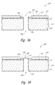
- FIGS. 3A-3D illustrate various stages in a method of forming the interconnects 236 in the microfeature workpiece 200 in accordance with an embodiment of the invention.
- FIG. 3A is a schematic side cross-sectional view of the area 3 A shown on FIG. 2 at an intermediate stage of forming the interconnect 236 .
- the microfeature workpiece 200 has a first dielectric layer 316 on the front side 212 of the substrate 210 and a second dielectric layer 317 on the first dielectric layer 316 .
- the second dielectric layer 317 has an opening 320 over the terminal 232 .
- the opening 320 can be etched into the second dielectric layer 317 to expose the terminal 232 .
- the first and second dielectric layers 316 and 317 are a polyimide material, but these dielectric layers can be other nonconductive materials in other embodiments.
- the first dielectric layer 316 and/or one or more subsequent dielectric layers can be a low temperature chemical vapor deposition (low temperature CVD) material, such as tetraethylorthosilicate (TEOS), parylene, silicon nitride (Si 3 Ni 4 ), silicon oxide (SiO 2 ), and/or other suitable materials.
- TEOS tetraethylorthosilicate
- parylene silicon nitride
- Si 3 Ni 4 silicon oxide
- SiO 2 silicon oxide
- the workpiece 200 also includes a via or passage 330 extending through the substrate 210 and the terminal 232 .
- the passage 330 includes a first portion 332 defined by the opening 333 at the front side 212 of the substrate 210 and a second portion 334 at the backside 214 of the substrate 210 .
- the passage 330 can be formed using a laser-cutting method at least generally similar to one or more of the methods described in U.S. patent application Ser. No. 10/713,878, entitled “Microelectronic Devices, Methods for Forming Vias in Microelectronic Devices, and Methods for Packaging Microelectronic Devices,” filed on Nov. 13, 2003, and incorporated herein in its entirety.
- the passage 330 can be formed using other methods, such as a suitable etching or drilling method.
- a third dielectric layer 318 is applied to the microfeature workpiece 200 to cover the sidewall of the passage 330 in the substrate 210 .
- the third dielectric layer 318 can be applied using CVD, PVD, atomic layer deposition (ALD), or other deposition processes.
- the third dielectric layer 318 generally completely coats the sidewall of the passage 330 , but in some embodiments the third dielectric layer 318 covers only a portion of the sidewall.
- the third dielectric layer 318 is applied to the entire microfeature workpiece 200 so that it covers the exposed portions of the substrate 210 , the terminal 232 , and the second dielectric layer 317 .
- the third dielectric layer 318 can be a low temperature CVD oxide, but in other embodiments the third dielectric layer 318 can be other suitable dielectric materials as described above.
- the third dielectric layer 318 electrically insulates the components of the substrate 210 proximate to the passage 330 from conductive material that is subsequently deposited into the passage 330 to form the interconnect 236 , as described in greater detail below.
- the method continues by removing portions of the third dielectric layer 318 from the horizontal and diagonal surfaces at the front side 212 of the workpiece 200 .
- the third dielectric layer 318 is etched using a process that preferentially removes material at a higher etch rate from horizontal surfaces and surfaces having horizontal components relative to the direction of the etchant.
- etching processes are spacer etches.
- different processes can be used to selectively remove nonvertical portions of the third dielectric layer 318 so that the vertical portions of the third dielectric layer 318 on the sidewalls in the passage 330 remain on the workpiece 200 .
- the method further includes forming a conductive cap 340 at the opening 333 to seal the first portion 332 of the passage 330 .
- the conductive cap 340 is plated onto the terminal 232 using an electroless plating process.
- the conductive cap 340 can be Ni that plates onto the terminal 232 until the first portion 332 of the passage 330 is “pinched-off.”
- the cap 340 seals the first portion 332 of the passage 330 .
- the conductive cap 340 includes other materials and/or is formed using other processes.
- the method continues by filling at least a portion of the passage 330 with a conductive material 350 to form the interconnect 236 .
- the fill material 350 is electrolytic nickel, electrolytic copper, electrolytic solder, electroless nickel, electroless copper, conductive polymer paste, molten solder, or other electrically conductive materials.
- Various processes can be used to deposit the fill material 350 into the passage 330 .
- a conductive element 370 is pressed against the conductive cap 340 and biased at an electrical potential to electroplate the conductive material 350 within the passage 330 in a “bottom-up” plating process.
- other methods may be used to bias the conductive cap 340 at an electrical potential suitable for electroplating material into the passage 330 , or other methods for filling vias known to those in the art may be used.
- the workpiece 200 with the conductive cap 340 has several advantages compared to conventional processes that leave the passage 330 open before depositing the conductive material into the passage 330 .
- One advantage of sealing the passage 330 with the conductive cap 340 is that it allows the workpiece 200 to be releasably secured to a vacuum chuck using suction, which enables the use of chemical-mechanical planarization (CMP) processes. In contrast, it is difficult to secure workpieces with open passages using vacuum chucks.
- CMP chemical-mechanical planarization
- Another advantage of using the conductive cap 340 to seal the end of the passage 330 is that it protects the passage 330 from other fabrication processes. For example, processes such as dry etching or subsequent film deposition can contaminate and/or damage the passage 330 and the substrate 210 . By sealing the passage 330 with the conductive cap 340 , contamination or damage to materials within the passage 330 is mitigated.
- the conductive cap 340 enables bottom-up plating.
- High-aspect vias, such as the passage 330 are generally very difficult to plate because plating using a conformal seed layer can cause pinch-off and voids.
- the conductive cap 340 in the present embodiment provides bottom-up electroplating for filling the passage 330 with the conductive material 350 .
- FIGS. 4A-4C are schematic side cross-sectional views illustrating various stages of a method for forming the interconnect 236 in the microfeature workpiece 200 of FIG. 2 in accordance with another embodiment of the invention.
- the initial stages of this method are at least generally similar to the steps described above with respect to FIG. 3A ; accordingly, like reference numbers refer to like components in FIGS. 3A and 4A .
- the workpiece 200 includes a passage 430 extending through the substrate 210 and the terminal 232 .
- the passage 430 differs from the passage 330 of FIG. 3A in that the passage 430 is slightly tapered.
- a third dielectric layer 418 is deposited onto the workpiece 200 to cover the sidewall of the passage 430 within the substrate 210 .
- the third dielectric layer 418 generally covers at least a portion of the terminal 232 and the second dielectric layer 317 in addition to the exposed portion of the substrate 210 in the passage 430 .
- the third dielectric layer 418 is etched to expose surfaces on the front and back of the workpiece 200 outside the passage 430 .
- the method includes forming a conductive cap 440 at a first portion 432 of the passage 430 adjacent to the terminal 232 .
- the conductive cap 440 is formed by depositing a gold stud bump at an opening 433 in the passage 430 to occlude the first portion 432 of the passage 430 .
- the conductive cap 440 that seals the first portion 432 of the passage 430 can be formed by depositing an aluminum wedge stud or a solder cap.
- the solder cap can be formed by depositing a solder ball, solder paste, or a solder preform at the first portion 432 of the passage 430 and then reflowing the solder to form the conductive cap 440 .
- the conductive cap 440 can include other electrically conductive materials, such as copper, palladium, and/or various solders.
- the conductive cap 440 can be formed using an electroplating process as described above with respect to FIG. 3C .
- the method proceeds by filling at least a portion of the passage 430 with a conductive material 450 to form the interconnect 236 .
- the fill material 450 is nickel, copper, solder, conductive polymer paste, or other electrically conductive materials.
- Various processes can be used to deposit the fill material 450 into the passage 430 .
- a conductive element 470 is pressed against the conductive cap 440 and biased at an electrical potential to electroplate the conductive material 450 within the passage 430 .
- other deposition methods can be used to bias the conductive cap 440 at an electrical potential suitable for electroplating material into the passage 430 .
- other methods known to those of skill in the art may be used to deposit the fill material 450 into the passage 430 .
- FIGS. 5A-5C are schematic side cross-sectional views illustrating various stages in a method of forming the interconnect 236 in the microfeature workpiece 200 of FIG. 2 in accordance with another embodiment of the invention.
- the initial stages of this method are at least generally similar to the steps described above with respect to FIG. 3A ; accordingly, like reference numbers refer to like components in FIGS. 3A and 5A .
- the workpiece 200 includes a passage 530 extending only partially through the substrate 210 .
- the passage 530 differs from the passage 330 of FIG. 3A in that the passage 530 is a blind hole.
- a “blind hole” refers to a hole or aperture that extends only partially through the substrate 210 .
- the passage 530 is etched to an intermediate depth within the substrate 210 .
- the passage 530 may be drilled using a laser or formed using other processes known to those of skill in the art.
- a third dielectric layer 518 is deposited onto the workpiece 200 to cover the sidewalls of the passage 530 in the substrate 210 .
- the third dielectric layer 518 can be one of the materials described above with respect to FIG. 3A . In other embodiments, the third dielectric layer 518 may be formed using other nonconductive materials.
- the method proceeds by forming a conductive cap 540 at a first portion 532 of the passage 530 adjacent to the terminal 232 .
- the conductive cap 540 is formed using any of the materials and processes described above with respect to FIGS. 3C and 4B .
- the backside 214 of the substrate 210 is thinned to expose a second portion 534 of the passage 530 .
- the backside 214 of the substrate 210 is thinned using CMP processes, dry etching processes, chemical etching, chemical polishing, backgrinding, or other suitable grinding processes known to those of skill in the art.
- the remaining portion of the passage 530 is filled with a conductive material 550 to form the interconnect 236 extending through the substrate 210 .
- the fill material 550 can be at least generally similar to the materials described above with respect to FIGS. 3D and 4C .
- the fill material 550 is deposited into the passage 530 using a bottom-up plating process. In other embodiments, different methods known to those of skill in the art may be used to deposit the fill material 550 into the passage 530 .
Abstract
Description
Claims (22)
Priority Applications (1)
| Application Number | Priority Date | Filing Date | Title |
|---|---|---|---|
| US12/419,029 US7829976B2 (en) | 2004-06-29 | 2009-04-06 | Microelectronic devices and methods for forming interconnects in microelectronic devices |
Applications Claiming Priority (4)
| Application Number | Priority Date | Filing Date | Title |
|---|---|---|---|
| US10/879,838 US7232754B2 (en) | 2004-06-29 | 2004-06-29 | Microelectronic devices and methods for forming interconnects in microelectronic devices |
| US11/416,824 US7329943B2 (en) | 2004-06-29 | 2006-05-03 | Microelectronic devices and methods for forming interconnects in microelectronic devices |
| US12/027,106 US7531453B2 (en) | 2004-06-29 | 2008-02-06 | Microelectronic devices and methods for forming interconnects in microelectronic devices |
| US12/419,029 US7829976B2 (en) | 2004-06-29 | 2009-04-06 | Microelectronic devices and methods for forming interconnects in microelectronic devices |
Related Parent Applications (1)
| Application Number | Title | Priority Date | Filing Date |
|---|---|---|---|
| US12/027,106 Continuation US7531453B2 (en) | 2004-06-29 | 2008-02-06 | Microelectronic devices and methods for forming interconnects in microelectronic devices |
Publications (2)
| Publication Number | Publication Date |
|---|---|
| US20090191701A1 US20090191701A1 (en) | 2009-07-30 |
| US7829976B2 true US7829976B2 (en) | 2010-11-09 |
Family
ID=35506443
Family Applications (4)
| Application Number | Title | Priority Date | Filing Date |
|---|---|---|---|
| US10/879,838 Active 2025-01-04 US7232754B2 (en) | 2004-06-29 | 2004-06-29 | Microelectronic devices and methods for forming interconnects in microelectronic devices |
| US11/416,824 Active US7329943B2 (en) | 2004-06-29 | 2006-05-03 | Microelectronic devices and methods for forming interconnects in microelectronic devices |
| US12/027,106 Active US7531453B2 (en) | 2004-06-29 | 2008-02-06 | Microelectronic devices and methods for forming interconnects in microelectronic devices |
| US12/419,029 Active US7829976B2 (en) | 2004-06-29 | 2009-04-06 | Microelectronic devices and methods for forming interconnects in microelectronic devices |
Family Applications Before (3)
| Application Number | Title | Priority Date | Filing Date |
|---|---|---|---|
| US10/879,838 Active 2025-01-04 US7232754B2 (en) | 2004-06-29 | 2004-06-29 | Microelectronic devices and methods for forming interconnects in microelectronic devices |
| US11/416,824 Active US7329943B2 (en) | 2004-06-29 | 2006-05-03 | Microelectronic devices and methods for forming interconnects in microelectronic devices |
| US12/027,106 Active US7531453B2 (en) | 2004-06-29 | 2008-02-06 | Microelectronic devices and methods for forming interconnects in microelectronic devices |
Country Status (1)
| Country | Link |
|---|---|
| US (4) | US7232754B2 (en) |
Cited By (16)
| Publication number | Priority date | Publication date | Assignee | Title |
|---|---|---|---|---|
| US20100264551A1 (en) * | 2009-04-20 | 2010-10-21 | International Business Machines Corporation | Three dimensional integrated circuit integration using dielectric bonding first and through via formation last |
| US20120038029A1 (en) * | 2010-08-10 | 2012-02-16 | Kabushiki Kaisha Toshiba | Semiconductor device and method of manufacturing the same |
| US20120139094A1 (en) * | 2010-12-02 | 2012-06-07 | Tessera Research Llc | Stacked microelectronic assembly having interposer connecting active chips |
| US8563403B1 (en) | 2012-06-27 | 2013-10-22 | International Business Machines Corporation | Three dimensional integrated circuit integration using alignment via/dielectric bonding first and through via formation last |
| US8587126B2 (en) | 2010-12-02 | 2013-11-19 | Tessera, Inc. | Stacked microelectronic assembly with TSVs formed in stages with plural active chips |
| US8610264B2 (en) | 2010-12-08 | 2013-12-17 | Tessera, Inc. | Compliant interconnects in wafers |
| US8610259B2 (en) | 2010-09-17 | 2013-12-17 | Tessera, Inc. | Multi-function and shielded 3D interconnects |
| US20140041922A1 (en) * | 2012-08-08 | 2014-02-13 | Subtron Technology Co., Ltd. | Package carrier and manufacturing method thereof |
| US8735205B2 (en) | 2007-03-05 | 2014-05-27 | Invensas Corporation | Chips having rear contacts connected by through vias to front contacts |
| US8736066B2 (en) | 2010-12-02 | 2014-05-27 | Tessera, Inc. | Stacked microelectronic assemby with TSVS formed in stages and carrier above chip |
| US8735287B2 (en) | 2007-07-31 | 2014-05-27 | Invensas Corp. | Semiconductor packaging process using through silicon vias |
| US8791575B2 (en) | 2010-07-23 | 2014-07-29 | Tessera, Inc. | Microelectronic elements having metallic pads overlying vias |
| US8796135B2 (en) | 2010-07-23 | 2014-08-05 | Tessera, Inc. | Microelectronic elements with rear contacts connected with via first or via middle structures |
| US8847380B2 (en) | 2010-09-17 | 2014-09-30 | Tessera, Inc. | Staged via formation from both sides of chip |
| US9070678B2 (en) | 2006-11-22 | 2015-06-30 | Tessera, Inc. | Packaged semiconductor chips with array |
| US9640437B2 (en) | 2010-07-23 | 2017-05-02 | Tessera, Inc. | Methods of forming semiconductor elements using micro-abrasive particle stream |
Families Citing this family (76)
| Publication number | Priority date | Publication date | Assignee | Title |
|---|---|---|---|---|
| US7091124B2 (en) | 2003-11-13 | 2006-08-15 | Micron Technology, Inc. | Methods for forming vias in microelectronic devices, and methods for packaging microelectronic devices |
| US8084866B2 (en) | 2003-12-10 | 2011-12-27 | Micron Technology, Inc. | Microelectronic devices and methods for filling vias in microelectronic devices |
| US20050247894A1 (en) | 2004-05-05 | 2005-11-10 | Watkins Charles M | Systems and methods for forming apertures in microfeature workpieces |
| US7232754B2 (en) * | 2004-06-29 | 2007-06-19 | Micron Technology, Inc. | Microelectronic devices and methods for forming interconnects in microelectronic devices |
| US7416913B2 (en) | 2004-07-16 | 2008-08-26 | Micron Technology, Inc. | Methods of manufacturing microelectronic imaging units with discrete standoffs |
| US7189954B2 (en) | 2004-07-19 | 2007-03-13 | Micron Technology, Inc. | Microelectronic imagers with optical devices and methods of manufacturing such microelectronic imagers |
| US7364934B2 (en) * | 2004-08-10 | 2008-04-29 | Micron Technology, Inc. | Microelectronic imaging units and methods of manufacturing microelectronic imaging units |
| US7419852B2 (en) * | 2004-08-27 | 2008-09-02 | Micron Technology, Inc. | Low temperature methods of forming back side redistribution layers in association with through wafer interconnects, semiconductor devices including same, and assemblies |
| US7083425B2 (en) | 2004-08-27 | 2006-08-01 | Micron Technology, Inc. | Slanted vias for electrical circuits on circuit boards and other substrates |
| US7300857B2 (en) | 2004-09-02 | 2007-11-27 | Micron Technology, Inc. | Through-wafer interconnects for photoimager and memory wafers |
| US7279407B2 (en) * | 2004-09-02 | 2007-10-09 | Micron Technology, Inc. | Selective nickel plating of aluminum, copper, and tungsten structures |
| TWI254425B (en) * | 2004-10-26 | 2006-05-01 | Advanced Semiconductor Eng | Chip package structure, chip packaging process, chip carrier and manufacturing process thereof |
| US7271482B2 (en) * | 2004-12-30 | 2007-09-18 | Micron Technology, Inc. | Methods for forming interconnects in microelectronic workpieces and microelectronic workpieces formed using such methods |
| US7795134B2 (en) | 2005-06-28 | 2010-09-14 | Micron Technology, Inc. | Conductive interconnect structures and formation methods using supercritical fluids |
| SG130061A1 (en) | 2005-08-24 | 2007-03-20 | Micron Technology Inc | Microelectronic devices and microelectronic support devices, and associated assemblies and methods |
| US7772115B2 (en) * | 2005-09-01 | 2010-08-10 | Micron Technology, Inc. | Methods for forming through-wafer interconnects, intermediate structures so formed, and devices and systems having at least one solder dam structure |
| US7262134B2 (en) | 2005-09-01 | 2007-08-28 | Micron Technology, Inc. | Microfeature workpieces and methods for forming interconnects in microfeature workpieces |
| US7863187B2 (en) | 2005-09-01 | 2011-01-04 | Micron Technology, Inc. | Microfeature workpieces and methods for forming interconnects in microfeature workpieces |
| US8154105B2 (en) * | 2005-09-22 | 2012-04-10 | International Rectifier Corporation | Flip chip semiconductor device and process of its manufacture |
| JP5222459B2 (en) * | 2005-10-18 | 2013-06-26 | 新光電気工業株式会社 | Semiconductor chip manufacturing method, multichip package |
| US7601567B2 (en) * | 2005-12-13 | 2009-10-13 | Samsung Mobile Display Co., Ltd. | Method of preparing organic thin film transistor, organic thin film transistor, and organic light-emitting display device including the organic thin film transistor |
| US7749899B2 (en) | 2006-06-01 | 2010-07-06 | Micron Technology, Inc. | Microelectronic workpieces and methods and systems for forming interconnects in microelectronic workpieces |
| US7629249B2 (en) * | 2006-08-28 | 2009-12-08 | Micron Technology, Inc. | Microfeature workpieces having conductive interconnect structures formed by chemically reactive processes, and associated systems and methods |
| US7902643B2 (en) | 2006-08-31 | 2011-03-08 | Micron Technology, Inc. | Microfeature workpieces having interconnects and conductive backplanes, and associated systems and methods |
| US7829438B2 (en) | 2006-10-10 | 2010-11-09 | Tessera, Inc. | Edge connect wafer level stacking |
| US8513789B2 (en) | 2006-10-10 | 2013-08-20 | Tessera, Inc. | Edge connect wafer level stacking with leads extending along edges |
| US7901989B2 (en) * | 2006-10-10 | 2011-03-08 | Tessera, Inc. | Reconstituted wafer level stacking |
| DE102006049562A1 (en) * | 2006-10-20 | 2008-04-24 | Qimonda Ag | Substrate e.g. germanium substrate, manufacturing method for use in semiconductor module, involves sealing channel with material e.g. gold, and filling channel with electrically conductive material e.g. copper |
| US7791199B2 (en) * | 2006-11-22 | 2010-09-07 | Tessera, Inc. | Packaged semiconductor chips |
| US7952195B2 (en) | 2006-12-28 | 2011-05-31 | Tessera, Inc. | Stacked packages with bridging traces |
| US7919410B2 (en) * | 2007-03-14 | 2011-04-05 | Aptina Imaging Corporation | Packaging methods for imager devices |
| US8586465B2 (en) * | 2007-06-07 | 2013-11-19 | United Test And Assembly Center Ltd | Through silicon via dies and packages |
| US8367471B2 (en) | 2007-06-15 | 2013-02-05 | Micron Technology, Inc. | Semiconductor assemblies, stacked semiconductor devices, and methods of manufacturing semiconductor assemblies and stacked semiconductor devices |
| KR100920039B1 (en) * | 2007-06-21 | 2009-10-07 | 주식회사 하이닉스반도체 | Stacked semiconductor package and method of manufacturing thereof |
| SG149710A1 (en) | 2007-07-12 | 2009-02-27 | Micron Technology Inc | Interconnects for packaged semiconductor devices and methods for manufacturing such devices |
| KR101458538B1 (en) | 2007-07-27 | 2014-11-07 | 테세라, 인코포레이티드 | A stacked microelectronic unit, and method of fabrication thereof |
| US8193092B2 (en) | 2007-07-31 | 2012-06-05 | Micron Technology, Inc. | Semiconductor devices including a through-substrate conductive member with an exposed end and methods of manufacturing such semiconductor devices |
| KR101533663B1 (en) | 2007-08-03 | 2015-07-03 | 테세라, 인코포레이티드 | Stack packages using reconstituted wafers |
| US8043895B2 (en) | 2007-08-09 | 2011-10-25 | Tessera, Inc. | Method of fabricating stacked assembly including plurality of stacked microelectronic elements |
| SG150410A1 (en) | 2007-08-31 | 2009-03-30 | Micron Technology Inc | Partitioned through-layer via and associated systems and methods |
| US7884015B2 (en) | 2007-12-06 | 2011-02-08 | Micron Technology, Inc. | Methods for forming interconnects in microelectronic workpieces and microelectronic workpieces formed using such methods |
| US8084854B2 (en) | 2007-12-28 | 2011-12-27 | Micron Technology, Inc. | Pass-through 3D interconnect for microelectronic dies and associated systems and methods |
| JP2009206506A (en) * | 2008-01-31 | 2009-09-10 | Sanyo Electric Co Ltd | Substrate for mounting element and its manufacturing method, semiconductor module and portable device mounted with the same |
| US20090212381A1 (en) * | 2008-02-26 | 2009-08-27 | Tessera, Inc. | Wafer level packages for rear-face illuminated solid state image sensors |
| US20100053407A1 (en) * | 2008-02-26 | 2010-03-04 | Tessera, Inc. | Wafer level compliant packages for rear-face illuminated solid state image sensors |
| US8018065B2 (en) * | 2008-02-28 | 2011-09-13 | Atmel Corporation | Wafer-level integrated circuit package with top and bottom side electrical connections |
| US8253230B2 (en) | 2008-05-15 | 2012-08-28 | Micron Technology, Inc. | Disabling electrical connections using pass-through 3D interconnects and associated systems and methods |
| US7919348B2 (en) * | 2008-06-13 | 2011-04-05 | Aptina Imaging Corporation | Methods for protecting imaging elements of photoimagers during back side processing |
| JP5639052B2 (en) | 2008-06-16 | 2014-12-10 | テッセラ,インコーポレイテッド | Edge stacking at wafer level |
| KR20100020718A (en) * | 2008-08-13 | 2010-02-23 | 삼성전자주식회사 | Semiconductor chip, stack structure, and methods of fabricating the semiconductor chip and the stack structure |
| JP5308145B2 (en) | 2008-12-19 | 2013-10-09 | ルネサスエレクトロニクス株式会社 | Semiconductor device |
| US8367516B2 (en) * | 2009-01-14 | 2013-02-05 | Taiwan Semiconductor Manufacturing Company, Ltd. | Laser bonding for stacking semiconductor substrates |
| FR2941561B1 (en) * | 2009-01-28 | 2011-05-13 | Commissariat Energie Atomique | METHOD FOR CLOSING CAVITY FOR AT LEAST ONE MICROELECTRONIC DEVICE |
| CN102422412A (en) | 2009-03-13 | 2012-04-18 | 德塞拉股份有限公司 | Stacked microelectronic assemblies having vias extending through bond pads |
| TWI466258B (en) * | 2009-04-10 | 2014-12-21 | Nanya Technology Corp | Conductive through connection and forming method thereof |
| US8445304B2 (en) * | 2009-06-02 | 2013-05-21 | Micralyne Inc. | Semi-conductor sensor fabrication |
| CN102576789B (en) | 2009-09-20 | 2016-08-24 | 维亚甘有限公司 | The wafer-class encapsulation of electronic device |
| US9502612B2 (en) | 2009-09-20 | 2016-11-22 | Viagan Ltd. | Light emitting diode package with enhanced heat conduction |
| US8101517B2 (en) * | 2009-09-29 | 2012-01-24 | Infineon Technologies Ag | Semiconductor device and method for making same |
| TWI405317B (en) * | 2010-03-04 | 2013-08-11 | Unimicron Technology Corp | Package substrate and fabrication method thereof |
| US8324511B1 (en) * | 2010-04-06 | 2012-12-04 | Amkor Technology, Inc. | Through via nub reveal method and structure |
| US20120220101A1 (en) * | 2010-08-27 | 2012-08-30 | Triune Ip Llc | Internal conductive layer |
| US8685793B2 (en) | 2010-09-16 | 2014-04-01 | Tessera, Inc. | Chip assembly having via interconnects joined by plating |
| US8686565B2 (en) | 2010-09-16 | 2014-04-01 | Tessera, Inc. | Stacked chip assembly having vertical vias |
| KR101059490B1 (en) | 2010-11-15 | 2011-08-25 | 테세라 리써치 엘엘씨 | Conductive pads defined by embedded traces |
| KR20120052734A (en) * | 2010-11-16 | 2012-05-24 | 삼성전자주식회사 | Semiconductor chips and methods of forming the same |
| KR20120090417A (en) | 2011-02-08 | 2012-08-17 | 삼성전자주식회사 | Semiconductor device and method of manufacturing a semiconductor device |
| CN102683514B (en) | 2011-03-06 | 2017-07-14 | 维亚甘有限公司 | LED package and manufacture method |
| TWI455271B (en) * | 2011-05-24 | 2014-10-01 | 矽品精密工業股份有限公司 | Semiconductor component and method of making same |
| US8809191B2 (en) * | 2011-12-13 | 2014-08-19 | Stats Chippac, Ltd. | Semiconductor device and method of forming UBM structure on back surface of TSV semiconductor wafer |
| US9281242B2 (en) | 2012-10-25 | 2016-03-08 | Nanya Technology Corp. | Through silicon via stacked structure and a method of manufacturing the same |
| JP6107357B2 (en) * | 2013-04-16 | 2017-04-05 | 富士通セミコンダクター株式会社 | Semiconductor device and manufacturing method of semiconductor device |
| JP2015177382A (en) * | 2014-03-15 | 2015-10-05 | キヤノン株式会社 | Device with element electrode connected with through-wiring, and manufacturing method thereof |
| US9761509B2 (en) * | 2015-12-29 | 2017-09-12 | United Microelectronics Corp. | Semiconductor device with throgh-substrate via and method for fabrication the semiconductor device |
| US9786593B1 (en) | 2016-04-11 | 2017-10-10 | Nanya Technology Corporation | Semiconductor device and method for forming the same |
| US11004779B2 (en) * | 2018-02-09 | 2021-05-11 | Advanced Semiconductor Engineering, Inc. | Semiconductor device package and a method of manufacturing the same |
Citations (471)
| Publication number | Priority date | Publication date | Assignee | Title |
|---|---|---|---|---|
| US2821959A (en) | 1956-03-29 | 1958-02-04 | Bell Telephone Labor Inc | Mass soldering of electrical assemblies |
| US3006318A (en) | 1958-03-26 | 1961-10-31 | Western Electric Co | Apparatus for applying solder coatings to surfaces |
| US3345134A (en) | 1962-04-21 | 1967-10-03 | Knapsack Ag | Process and apparatus for the manufacture of titanium nitride |
| US3865298A (en) | 1973-08-14 | 1975-02-11 | Atomic Energy Commission | Solder leveling |
| US4040168A (en) | 1975-11-24 | 1977-08-09 | Rca Corporation | Fabrication method for a dual gate field-effect transistor |
| US4368106A (en) | 1980-10-27 | 1983-01-11 | General Electric Company | Implantation of electrical feed-through conductors |
| EP0127946A1 (en) | 1983-05-10 | 1984-12-12 | BRITISH TELECOMMUNICATIONS public limited company | Method of producing a via in a semiconductor device |
| US4534100A (en) | 1982-06-28 | 1985-08-13 | The United States Of America As Represented By The Secretary Of The Air Force | Electrical method of making conductive paths in silicon |
| US4581301A (en) | 1984-04-10 | 1986-04-08 | Michaelson Henry W | Additive adhesive based process for the manufacture of printed circuit boards |
| US4608480A (en) | 1983-06-15 | 1986-08-26 | S.N.E.C.M.A. | Process and apparatus for laser drilling |
| US4614427A (en) | 1983-05-20 | 1986-09-30 | Hitachi, Ltd. | Automatic contaminants detection apparatus |
| US4660063A (en) | 1985-03-18 | 1987-04-21 | General Electric Company | Immersion type ISFET |
| JPS6352432A (en) | 1986-08-22 | 1988-03-05 | Hitachi Vlsi Eng Corp | Semiconductor device |
| US4756765A (en) | 1982-01-26 | 1988-07-12 | Avco Research Laboratory, Inc. | Laser removal of poor thermally-conductive materials |
| US4768291A (en) | 1987-03-12 | 1988-09-06 | Monarch Technologies Corporation | Apparatus for dry processing a semiconductor wafer |
| US4906314A (en) | 1988-12-30 | 1990-03-06 | Micron Technology, Inc. | Process for simultaneously applying precut swatches of precured polyimide film to each semiconductor die on a wafer |
| US4959705A (en) | 1988-10-17 | 1990-09-25 | Ford Microelectronics, Inc. | Three metal personalization of application specific monolithic microwave integrated circuit |
| US4964212A (en) | 1988-09-29 | 1990-10-23 | Commissariat A L'energie Atomique | Process for producing electrical connections through a substrate |
| US4984597A (en) | 1984-05-21 | 1991-01-15 | Cfm Technologies Research Associates | Apparatus for rinsing and drying surfaces |
| US5024966A (en) | 1988-12-21 | 1991-06-18 | At&T Bell Laboratories | Method of forming a silicon-based semiconductor optical device mount |
| US5027184A (en) | 1981-03-02 | 1991-06-25 | Rockwell International Corporation | NPN type lateral transistor with minimal substrate operation interference |
| US5026964A (en) | 1986-02-28 | 1991-06-25 | General Electric Company | Optical breakthrough sensor for laser drill |
| US5037782A (en) | 1989-03-29 | 1991-08-06 | Mitsubishi Denki Kabushiki Kaisha | Method of making a semiconductor device including via holes |
| US5123902A (en) | 1988-09-13 | 1992-06-23 | Carl-Zeiss-Stiftung | Method and apparatus for performing surgery on tissue wherein a laser beam is applied to the tissue |
| US5130783A (en) | 1991-03-04 | 1992-07-14 | Texas Instruments Incorporated | Flexible film semiconductor package |
| US5145099A (en) | 1990-07-13 | 1992-09-08 | Micron Technology, Inc. | Method for combining die attach and lead bond in the assembly of a semiconductor package |
| US5158911A (en) | 1990-08-03 | 1992-10-27 | Thomson Composants Microondes | Method for interconnection between an integrated circuit and a support circuit, and integrated circuit adapted to this method |
| US5219344A (en) | 1988-06-09 | 1993-06-15 | Visx, Incorporated | Methods and apparatus for laser sculpture of the cornea |
| US5233448A (en) | 1992-05-04 | 1993-08-03 | Industrial Technology Research Institute | Method of manufacturing a liquid crystal display panel including photoconductive electrostatic protection |
| US5237148A (en) | 1990-10-04 | 1993-08-17 | Brother Kogyo Kabushiki | Device for manufacturing a nozzle and its manufacturing method |
| US5289631A (en) | 1992-03-04 | 1994-03-01 | Mcnc | Method for testing, burn-in, and/or programming of integrated circuit chips |
| US5292686A (en) | 1991-08-21 | 1994-03-08 | Triquint Semiconductor, Inc. | Method of forming substrate vias in a GaAs wafer |
| US5294568A (en) | 1990-10-12 | 1994-03-15 | Genus, Inc. | Method of selective etching native oxide |
| US5371397A (en) | 1992-10-09 | 1994-12-06 | Mitsubishi Denki Kabushiki Kaisha | Solid-state imaging array including focusing elements |
| US5378312A (en) | 1993-12-07 | 1995-01-03 | International Business Machines Corporation | Process for fabricating a semiconductor structure having sidewalls |
| US5378313A (en) | 1993-12-22 | 1995-01-03 | Pace; Benedict G. | Hybrid circuits and a method of manufacture |
| US5380681A (en) | 1994-03-21 | 1995-01-10 | United Microelectronics Corporation | Three-dimensional multichip package and methods of fabricating |
| US5402435A (en) | 1993-03-05 | 1995-03-28 | Matsushita Electric Industrial Co., Ltd. | Optical device |
| US5406630A (en) | 1992-05-04 | 1995-04-11 | Motorola, Inc. | Tamperproof arrangement for an integrated circuit device |
| US5424573A (en) | 1992-03-04 | 1995-06-13 | Hitachi, Ltd. | Semiconductor package having optical interconnection access |
| TW250597B (en) | 1993-06-04 | 1995-07-01 | Framatome & Cie | |
| US5435887A (en) | 1993-11-03 | 1995-07-25 | Massachusetts Institute Of Technology | Methods for the fabrication of microstructure arrays |
| US5438212A (en) | 1993-02-25 | 1995-08-01 | Mitsubishi Denki Kabushiki Kaisha | Semiconductor device with heat dissipation structure |
| US5447871A (en) | 1993-03-05 | 1995-09-05 | Goldstein; Edward F. | Electrically conductive interconnection through a body of semiconductor material |
| US5464960A (en) | 1993-01-12 | 1995-11-07 | Iatrotech, Inc. | Laser calibration device |
| US5481483A (en) | 1992-11-23 | 1996-01-02 | Ford Motor Company | Non-contact method of obtaining dimensional information about an object for comparing similar objects |
| US5496755A (en) | 1989-11-29 | 1996-03-05 | Texas Instruments Incorporated | Integrated circuit and method |
| US5505804A (en) | 1993-12-24 | 1996-04-09 | Sharp Kabushiki Kaisha | Method of producing a condenser lens substrate |
| US5518956A (en) | 1993-09-02 | 1996-05-21 | General Electric Company | Method of isolating vertical shorts in an electronic array using laser ablation |
| US5585675A (en) | 1994-05-11 | 1996-12-17 | Harris Corporation | Semiconductor die packaging tub having angularly offset pad-to-pad via structure configured to allow three-dimensional stacking and electrical interconnections among multiple identical tubs |
| US5585308A (en) | 1993-12-23 | 1996-12-17 | Sgs-Thomson Microelectronics, Inc. | Method for improved pre-metal planarization |
| US5593913A (en) | 1993-09-28 | 1997-01-14 | Sharp Kabushiki Kaisha | Method of manufacturing solid state imaging device having high sensitivity and exhibiting high degree of light utilization |
| US5605783A (en) | 1995-01-06 | 1997-02-25 | Eastman Kodak Company | Pattern transfer techniques for fabrication of lenslet arrays for solid state imagers |
| US5614743A (en) | 1994-07-26 | 1997-03-25 | Kabushiki Kaisha Toshiba | Microwave integrated circuit (MIC) having a reactance element formed on a groove |
| US5618752A (en) | 1995-06-05 | 1997-04-08 | Harris Corporation | Method of fabrication of surface mountable integrated circuits |
| US5624437A (en) | 1995-03-28 | 1997-04-29 | Freeman; Jerre M. | High resolution, high speed, programmable laser beam modulating apparatus for microsurgery |
| US5627106A (en) | 1994-05-06 | 1997-05-06 | United Microelectronics Corporation | Trench method for three dimensional chip connecting during IC fabrication |
| US5646067A (en) | 1995-06-05 | 1997-07-08 | Harris Corporation | Method of bonding wafers having vias including conductive material |
| US5654221A (en) | 1994-10-17 | 1997-08-05 | International Business Machines Corporation | Method for forming semiconductor chip and electronic module with integrated surface interconnects/components |
| US5672519A (en) | 1994-02-23 | 1997-09-30 | Lg Semicon Co., Ltd. | Method of fabricating solid state image sensing elements |
| US5673846A (en) | 1995-08-24 | 1997-10-07 | International Business Machines Corporation | Solder anchor decal and method |
| US5684642A (en) | 1994-02-22 | 1997-11-04 | Mitsubishi Denki Kabushiki Kaisha | Optical transmission system and light radiating method |
| US5690841A (en) | 1993-12-10 | 1997-11-25 | Pharmacia Biotech Ab | Method of producing cavity structures |
| US5694246A (en) | 1994-01-03 | 1997-12-02 | Omron Corporation | Method of manufacturing lens array |
| US5708293A (en) | 1996-01-05 | 1998-01-13 | Matsushita Electronics Corporation | Lead frame and method of mounting semiconductor chip |
| US5718791A (en) | 1995-06-05 | 1998-02-17 | R + S Stanztechnik Gmbh | Method of laminating a trim panel and folding a cover sheet edge around the panel rim |
| US5723904A (en) | 1993-03-10 | 1998-03-03 | Sumitomo Electric Industries, Ltd. | Packaged semiconductor device suitable to be mounted and connected to microstrip line structure board |
| US5726493A (en) | 1994-06-13 | 1998-03-10 | Fujitsu Limited | Semiconductor device and semiconductor device unit having ball-grid-array type package structure |
| US5771158A (en) | 1995-09-21 | 1998-06-23 | Mitsubishi Denki Kabushiki Kaisha | Printed circuit board, printed circuit board used for flat panel display drive circuit, and flat panel display device |
| US5773359A (en) | 1995-12-26 | 1998-06-30 | Motorola, Inc. | Interconnect system and method of fabrication |
| US5776824A (en) | 1995-12-22 | 1998-07-07 | Micron Technology, Inc. | Method for producing laminated film/metal structures for known good die ("KG") applications |
| US5807439A (en) | 1997-09-29 | 1998-09-15 | Siemens Aktiengesellschaft | Apparatus and method for improved washing and drying of semiconductor wafers |
| US5811799A (en) | 1997-07-31 | 1998-09-22 | Wu; Liang-Chung | Image sensor package having a wall with a sealed cover |
| US5821532A (en) | 1997-06-16 | 1998-10-13 | Eastman Kodak Company | Imager package substrate |
| US5825080A (en) | 1995-12-18 | 1998-10-20 | Atr Optical And Radio Communications Research Laboratories | Semiconductor device provided with surface grounding conductor for covering surfaces of electrically insulating films |
| US5826628A (en) | 1996-01-24 | 1998-10-27 | Micron Technology, Inc. | Form tooling and method of forming semiconductor package leads |
| US5847454A (en) | 1993-02-04 | 1998-12-08 | Cornell Research Foundcatton, Inc. | Electrically isolated released microstructures |
| US5851845A (en) | 1995-12-18 | 1998-12-22 | Micron Technology, Inc. | Process for packaging a semiconductor die using dicing and testing |
| US5857963A (en) | 1996-07-17 | 1999-01-12 | Welch Allyn, Inc. | Tab imager assembly for use in an endoscope |
| US5861654A (en) | 1995-11-28 | 1999-01-19 | Eastman Kodak Company | Image sensor assembly |
| US5870289A (en) | 1994-12-15 | 1999-02-09 | Hitachi, Ltd. | Chip connection structure having diret through-hole connections through adhesive film and wiring substrate |
| US5870823A (en) | 1996-11-27 | 1999-02-16 | International Business Machines Corporation | Method of forming a multilayer electronic packaging substrate with integral cooling channels |
| US5877040A (en) | 1995-08-10 | 1999-03-02 | Lg Semicon Co., Ltd. | Method of making charge-coupled device with microlens |
| US5893828A (en) | 1996-05-02 | 1999-04-13 | Uram; Martin | Contact laser surgical endoscope and associated myringotomy procedure |
| US5897338A (en) | 1996-06-11 | 1999-04-27 | European Semiconductor Assembly (Eurasem) B.V. | Method for encapsulating an integrated semi-conductor circuit |
| US5904499A (en) | 1994-12-22 | 1999-05-18 | Pace; Benedict G | Package for power semiconductor chips |
| US5914488A (en) | 1996-03-05 | 1999-06-22 | Mitsubishi Denki Kabushiki Kaisha | Infrared detector |
| US5977535A (en) | 1992-09-30 | 1999-11-02 | Lsi Logic Corporation | Light sensing device having an array of photosensitive elements coincident with an array of lens formed on an optically transmissive material |
| US5998862A (en) | 1993-03-26 | 1999-12-07 | Sony Corporation | Air-packed CCD images package and a mold for manufacturing thereof |
| US5998240A (en) | 1996-07-22 | 1999-12-07 | Northrop Grumman Corporation | Method of extracting heat from a semiconductor body and forming microchannels therein |
| US5998292A (en) | 1997-11-12 | 1999-12-07 | International Business Machines Corporation | Method for making three dimensional circuit integration |
| US6004867A (en) | 1996-12-16 | 1999-12-21 | Samsung Electronics Co., Ltd. | Chip-size packages assembled using mass production techniques at the wafer-level |
| US6008070A (en) | 1998-05-21 | 1999-12-28 | Micron Technology, Inc. | Wafer level fabrication and assembly of chip scale packages |
| US6080291A (en) | 1998-07-10 | 2000-06-27 | Semitool, Inc. | Apparatus for electrochemically processing a workpiece including an electrical contact assembly having a seal member |
| US6097087A (en) | 1997-10-31 | 2000-08-01 | Micron Technology, Inc. | Semiconductor package including flex circuit, interconnects and dense array external contacts |
| US6104086A (en) | 1997-05-20 | 2000-08-15 | Nec Corporation | Semiconductor device having lead terminals bent in J-shape |
| US6103547A (en) | 1997-01-17 | 2000-08-15 | Micron Technology, Inc. | High speed IC package configuration |
| US6107679A (en) | 1997-12-22 | 2000-08-22 | Oki Electric Industry Co., Ltd. | Semiconductor device |
| US6107180A (en) | 1998-01-30 | 2000-08-22 | Motorola, Inc. | Method for forming interconnect bumps on a semiconductor die |
| US6110825A (en) | 1997-11-26 | 2000-08-29 | Stmicroelectronics, S.R.L. | Process for forming front-back through contacts in micro-integrated electronic devices |
| US6114240A (en) | 1997-12-18 | 2000-09-05 | Micron Technology, Inc. | Method for fabricating semiconductor components using focused laser beam |
| US6119335A (en) | 1997-12-02 | 2000-09-19 | Samsung Electro-Mechanics Co., Ltd. | Method for manufacturing multi-layer printed circuit board |
| US6124634A (en) | 1996-03-07 | 2000-09-26 | Micron Technology, Inc. | Micromachined chip scale package |
| US6130141A (en) | 1998-10-14 | 2000-10-10 | Lucent Technologies Inc. | Flip chip metallization |
| US6137182A (en) | 1996-07-23 | 2000-10-24 | Advanced Micro Devices, Inc. | Method of reducing via and contact dimensions beyond photolithography equipment limits |
| US6140604A (en) | 1998-06-18 | 2000-10-31 | General Electric Company | Laser drilling breakthrough detector |
| US6143588A (en) | 1997-09-09 | 2000-11-07 | Amkor Technology, Inc. | Method of making an integrated circuit package employing a transparent encapsulant |
| US6148509A (en) | 1997-04-07 | 2000-11-21 | Micron Technology, Inc. | Method for supporting an integrated circuit die |
| US6159764A (en) | 1997-07-02 | 2000-12-12 | Micron Technology, Inc. | Varied-thickness heat sink for integrated circuit (IC) packages and method of fabricating IC packages |
| US6180518B1 (en) | 1999-10-29 | 2001-01-30 | Lucent Technologies Inc. | Method for forming vias in a low dielectric constant material |
| US6184465B1 (en) | 1998-11-12 | 2001-02-06 | Micron Technology, Inc. | Semiconductor package |
| US6184060B1 (en) | 1996-10-29 | 2001-02-06 | Trusi Technologies Llc | Integrated circuits and methods for their fabrication |
| US6187615B1 (en) | 1998-08-28 | 2001-02-13 | Samsung Electronics Co., Ltd. | Chip scale packages and methods for manufacturing the chip scale packages at wafer level |
| US6191487B1 (en) | 1998-04-23 | 2001-02-20 | Minco Technology Labs, Inc. | Semiconductor and flip chip packages and method having a back-side connection |
| KR20010018694A (en) | 1999-08-21 | 2001-03-15 | 윤종용 | Manufacturing method for three demensional stack chip package |
| US6203539B1 (en) | 1993-05-07 | 2001-03-20 | Visx, Incorporated | Method and system for laser treatment of refractive errors using offset imaging |
| JP2001077496A (en) | 1999-09-06 | 2001-03-23 | Ngk Insulators Ltd | Substrate for printed circuit and its manufacture |
| JP2001082931A (en) | 1999-09-09 | 2001-03-30 | Toshiba Corp | Method and apparatus for measuring depth of hole |
| US6222136B1 (en) | 1997-11-12 | 2001-04-24 | International Business Machines Corporation | Printed circuit board with continuous connective bumps |
| US6222270B1 (en) | 1997-06-24 | 2001-04-24 | Samsung Electronics Co., Ltd. | Integrated circuit bonding pads including closed vias and closed conductive patterns |
| US6229202B1 (en) | 2000-01-10 | 2001-05-08 | Micron Technology, Inc. | Semiconductor package having downset leadframe for reducing package bow |
| US6228687B1 (en) | 1999-06-28 | 2001-05-08 | Micron Technology, Inc. | Wafer-level package and methods of fabricating |
| US6235552B1 (en) | 1999-07-09 | 2001-05-22 | Samsung Electronics Co., Ltd. | Chip scale package and method for manufacturing the same using a redistribution substrate |
| US6236046B1 (en) | 1997-10-28 | 2001-05-22 | Matsushita Electric Works, Ltd. | Infrared sensor |
| US6246108B1 (en) | 1997-09-15 | 2001-06-12 | Micron Technology, Inc. | Integrated circuit package including lead frame with electrically isolated alignment feature |
| US6252300B1 (en) | 1999-01-14 | 2001-06-26 | United Microelectronics Corp. | Direct contact through hole type wafer structure |
| US6259083B1 (en) | 1997-08-13 | 2001-07-10 | Sony Corporation | Solid state imaging device and manufacturing method thereof |
| US6266197B1 (en) | 1999-12-08 | 2001-07-24 | Amkor Technology, Inc. | Molded window array for image sensor packages |
| US6268114B1 (en) | 1998-09-18 | 2001-07-31 | Taiwan Semiconductor Manufacturing Company, Ltd | Method for forming fine-pitched solder bumps |
| US6271580B1 (en) | 1996-12-30 | 2001-08-07 | Micron Technology, Inc. | Leads under chip in conventional IC package |
| US6274927B1 (en) | 1999-06-03 | 2001-08-14 | Amkor Technology, Inc. | Plastic package for an optical integrated circuit device and method of making |
| US6277757B1 (en) | 1999-06-01 | 2001-08-21 | Winbond Electronics Corp. | Methods to modify wet by dry etched via profile |
| US6285064B1 (en) | 2000-03-28 | 2001-09-04 | Omnivision Technologies, Inc. | Chip scale packaging technique for optical image sensing integrated circuits |
| US20010020739A1 (en) | 2000-03-09 | 2001-09-13 | Nec Corporation | Flip chip type semiconductor device and method for manufacturing the same |
| US6291894B1 (en) | 1998-08-31 | 2001-09-18 | Micron Technology, Inc. | Method and apparatus for a semiconductor package for vertical surface mounting |
| US6294837B1 (en) | 1997-12-18 | 2001-09-25 | Micron Technology, Inc. | Semiconductor interconnect having laser machined contacts |
| JP2001298147A (en) | 2000-04-18 | 2001-10-26 | Kawasaki Steel Corp | Semiconductor device and its manufacturing method |
| EP1154474A1 (en) | 1999-08-23 | 2001-11-14 | Rohm Co., Ltd. | Semiconductor device and method of manufacture thereof |
| US6326689B1 (en) | 1999-07-26 | 2001-12-04 | Stmicroelectronics, Inc. | Backside contact for touchchip |
| US6329632B1 (en) | 1998-07-30 | 2001-12-11 | Societe Nationale d'Etude et de Construction de Moteurs d'Aviation “SNECMA” | Method and device for machining holes or shapes of varying profile using an excimer laser |
| US20020005583A1 (en) | 2000-06-07 | 2002-01-17 | Mitsubishi Denki Kabushiki Kaisha | Semiconductor device and fabrication process therefor |
| US20020006687A1 (en) | 2000-05-23 | 2002-01-17 | Lam Ken M. | Integrated IC chip package for electronic image sensor die |
| US6341009B1 (en) | 2000-02-24 | 2002-01-22 | Quantronix Corporation | Laser delivery system and method for photolithographic mask repair |
| US6344976B1 (en) | 1997-04-07 | 2002-02-05 | Micron Technology, Inc. | Interdigitated leads-over-chip lead frame device and method for supporting an integrated circuit die |
| US20020020898A1 (en) | 2000-08-16 | 2002-02-21 | Vu Quat T. | Microelectronic substrates with integrated devices |
| US6351027B1 (en) | 2000-02-29 | 2002-02-26 | Agilent Technologies, Inc. | Chip-mounted enclosure |
| US20020027293A1 (en) | 2001-06-28 | 2002-03-07 | Fujitsu Limited | Three dimensional semiconductor integrated circuit device and method for making the same |
| US6359254B1 (en) | 1999-09-30 | 2002-03-19 | United Technologies Corporation | Method for producing shaped hole in a structure |
| US6359328B1 (en) | 1998-12-31 | 2002-03-19 | Intel Corporation | Methods for making interconnects and diffusion barriers in integrated circuits |
| KR20020022122A (en) | 2000-07-27 | 2002-03-25 | 크리스띠앙 쥘랭 | Process for fabricating a multilevel circuitry comprising tracks and microvias |
| US6372548B2 (en) | 1998-06-04 | 2002-04-16 | Matsushita Electric Industrial Co., Ltd. | Method for fabricating a semiconductor package with a semiconductor device attached to a multilayered substrate |
| US6388208B1 (en) | 1999-06-11 | 2002-05-14 | Teradyne, Inc. | Multi-connection via with electrically isolated segments |
| US20020057468A1 (en) | 2000-11-14 | 2002-05-16 | Masao Segawa | Image pickup apparatus, method thereof, and electric apparatus |
| US6391770B2 (en) | 1997-04-24 | 2002-05-21 | Mitsubishi Denki Kabushiki Kaisha | Method of manufacturing semiconductor device |
| US20020059722A1 (en) | 1995-07-27 | 2002-05-23 | Nec Corporation | Method of mounting a semiconductor device to a substrate and a mounted structure |
| US20020060208A1 (en) | 1999-12-23 | 2002-05-23 | Xinbing Liu | Apparatus for drilling holes with sub-wavelength pitch with laser |
| US6406636B1 (en) | 1999-06-02 | 2002-06-18 | Megasense, Inc. | Methods for wafer to wafer bonding using microstructures |
| US6407381B1 (en) | 2000-07-05 | 2002-06-18 | Amkor Technology, Inc. | Wafer scale image sensor package |
| US6411439B2 (en) | 1998-05-19 | 2002-06-25 | Seiko Epson Corporation | Microlens array, a manufacturing method therefor, and a display apparatus using the same |
| US20020089025A1 (en) | 2001-01-05 | 2002-07-11 | Li-Kun Chou | Package structure for image IC |
| US20020094607A1 (en) | 2001-01-16 | 2002-07-18 | Uta Gebauer | Electronic component with stacked semiconductor chips and method of producing the component |
| KR20020061812A (en) | 2001-01-18 | 2002-07-25 | 삼성전자 주식회사 | Ball grid array type multi chip package and stack package |
| US20020096729A1 (en) | 2001-01-24 | 2002-07-25 | Tu Hsiu Wen | Stacked package structure of image sensor |
| US6433304B2 (en) | 1999-12-22 | 2002-08-13 | Honda Giken Kogyo Kabushiki Kaisha | Perforating machining method with laser beam |
| US6433303B1 (en) | 2000-03-31 | 2002-08-13 | Matsushita Electric Industrial Co., Ltd. | Method and apparatus using laser pulses to make an array of microcavity holes |
| US6437441B1 (en) | 1997-07-10 | 2002-08-20 | Kawasaki Microelectronics, Inc. | Wiring structure of a semiconductor integrated circuit and a method of forming the wiring structure |
| US6437284B1 (en) | 1999-06-25 | 2002-08-20 | Mitsubishi Denki Kabushiki Kaisha | Optical system and apparatus for laser heat treatment and method for producing semiconductor devices by using the same |
| US20020113296A1 (en) | 2001-02-03 | 2002-08-22 | Samsung Electronics Co., Ltd. | Wafer level hermetic sealing method |
| US6441487B2 (en) | 1997-10-20 | 2002-08-27 | Flip Chip Technologies, L.L.C. | Chip scale package using large ductile solder balls |
| US6452270B1 (en) | 2000-10-13 | 2002-09-17 | Advanced Semiconductor Engineering, Inc. | Semiconductor device having bump electrode |
| US20020130390A1 (en) | 2001-03-13 | 2002-09-19 | Ming-Dou Ker | ESD protection circuit with very low input capacitance for high-frequency I/O ports |
| US6457515B1 (en) | 1999-08-06 | 2002-10-01 | The Ohio State University | Two-layered micro channel heat sink, devices and systems incorporating same |
| US6459150B1 (en) | 2000-08-17 | 2002-10-01 | Industrial Technology Research Institute | Electronic substrate having an aperture position through a substrate, conductive pads, and an insulating layer |
| US6459039B1 (en) | 2000-06-19 | 2002-10-01 | International Business Machines Corporation | Method and apparatus to manufacture an electronic package with direct wiring pattern |
| US20020145676A1 (en) | 2001-02-26 | 2002-10-10 | Tetsuya Kuno | Image pickup apparatus |
| US6468889B1 (en) | 2000-08-08 | 2002-10-22 | Advanced Micro Devices, Inc. | Backside contact for integrated circuit and method of forming same |
| US6483652B2 (en) | 2000-08-17 | 2002-11-19 | Sharp Kabushiki Kaisha | Method for producing solid-state imaging device |
| US6486083B1 (en) | 2000-02-15 | 2002-11-26 | Kokusai Electric Co., Ltd. | Semiconductor device manufacturing method and semiconductor manufacturing apparatus |
| US6486549B1 (en) | 2001-11-10 | 2002-11-26 | Bridge Semiconductor Corporation | Semiconductor module with encapsulant base |
| US20020190371A1 (en) | 2001-06-14 | 2002-12-19 | Shinko Electric Industries Co., Ltd. | Semiconductor device and method of production of same |
| US6503780B1 (en) | 2000-07-05 | 2003-01-07 | Amkor Technology, Inc. | Wafer scale image sensor package fabrication method |
| US20030014895A1 (en) | 1999-10-08 | 2003-01-23 | Lizotte Todd E. | Control system for ablating high-density array of vias or indentation in surface of object |
| US6521516B2 (en) | 2001-06-29 | 2003-02-18 | Intel Corporation | Process for local on-chip cooling of semiconductor devices using buried microchannels |
| US6521530B2 (en) | 1998-11-13 | 2003-02-18 | Fujitsu Limited | Composite interposer and method for producing a composite interposer |
| US20030042564A1 (en) | 2000-12-04 | 2003-03-06 | Fujitsu Limited | Semiconductor device having an interconnecting post formed on an interposer within a sealing resin |
| US6534192B1 (en) | 1999-09-24 | 2003-03-18 | Lucent Technologies Inc. | Multi-purpose finish for printed wiring boards and method of manufacture of such boards |
| US6534863B2 (en) | 2001-02-09 | 2003-03-18 | International Business Machines Corporation | Common ball-limiting metallurgy for I/O sites |
| US6541762B2 (en) | 2001-08-14 | 2003-04-01 | Samsung Electro-Mechanics Co., Ltd. | Sub chip on board for optical mouse |
| US20030062601A1 (en) | 2001-05-15 | 2003-04-03 | James Harnden | Surface mount package |
| US6545563B1 (en) | 1990-07-16 | 2003-04-08 | Raytheon Company | Digitally controlled monolithic microwave integrated circuits |
| US6555782B2 (en) | 1997-12-12 | 2003-04-29 | Matsushita Electric Industrial Co., Ltd. | Laser machining method, laser machining apparatus, and its control method |
| US6560047B2 (en) | 2001-08-29 | 2003-05-06 | Samsung Electro-Mechanics Co., Ltd. | Image module |
| US6566745B1 (en) | 1999-03-29 | 2003-05-20 | Imec Vzw | Image sensor ball grid array package and the fabrication thereof |
| US6569777B1 (en) | 2002-10-02 | 2003-05-27 | Taiwan Semiconductor Manufacturing Co., Ltd | Plasma etching method to form dual damascene with improved via profile |
| US6569711B1 (en) | 1998-04-28 | 2003-05-27 | International Business Machines Corporation | Methods and apparatus for balancing differences in thermal expansion in electronic packaging |
| US6572606B2 (en) | 2000-01-12 | 2003-06-03 | Lasersight Technologies, Inc. | Laser fluence compensation of a curved surface |
| US6576531B2 (en) | 2001-08-24 | 2003-06-10 | Micron Technology, Inc. | Method for cutting semiconductor wafers |
| US6580174B2 (en) | 2001-09-28 | 2003-06-17 | Intel Corporation | Vented vias for via in pad technology yield improvements |
| US6582987B2 (en) | 2000-12-30 | 2003-06-24 | Electronics And Telecommunications Research Institute | Method of fabricating microchannel array structure embedded in silicon substrate |
| US20030119308A1 (en) | 2001-12-20 | 2003-06-26 | Geefay Frank S. | Sloped via contacts |
| US6593644B2 (en) | 2001-04-19 | 2003-07-15 | International Business Machines Corporation | System of a package fabricated on a semiconductor or dielectric wafer with wiring on one face, vias extending through the wafer, and external connections on the opposing face |
| US6599436B1 (en) | 2001-12-06 | 2003-07-29 | Sandia Corporation | Formation of interconnections to microfluidic devices |
| US6603183B1 (en) | 2001-09-04 | 2003-08-05 | Amkor Technology, Inc. | Quick sealing glass-lidded package |
| US20030148597A1 (en) | 2002-01-09 | 2003-08-07 | Tan Hock Chuan | Stacked die in die BGA package |
| US6606251B1 (en) | 2002-02-07 | 2003-08-12 | Cooligy Inc. | Power conditioning module |
| US6614033B2 (en) | 1998-04-17 | 2003-09-02 | Kabushiki Kaisha Toshiba | Ion implantation apparatus, ion generating apparatus and semiconductor manufacturing method with ion implantation processes |
| US6617623B2 (en) | 1999-06-15 | 2003-09-09 | Micron Technology, Inc. | Multi-layered gate for a CMOS imager |
| US6620731B1 (en) | 1997-12-18 | 2003-09-16 | Micron Technology, Inc. | Method for fabricating semiconductor components and interconnects with contacts on opposing sides |
| US6638410B2 (en) | 1998-03-20 | 2003-10-28 | Semitool, Inc. | Apparatus and method for electrolytically depositing copper on a semiconductor workpiece |
| US20030216023A1 (en) | 1997-03-26 | 2003-11-20 | Wark James M. | Projected contact structures for engaging bumped semiconductor devices and methods of making the same |
| US6653236B2 (en) | 2002-03-29 | 2003-11-25 | Micron Technology, Inc. | Methods of forming metal-containing films over surfaces of semiconductor substrates; and semiconductor constructions |
| US6660630B1 (en) | 2002-10-10 | 2003-12-09 | Taiwan Semiconductor Manufacturing Co. Ltd. | Method for forming a tapered dual damascene via portion with improved performance |
| US6661047B2 (en) | 2001-08-30 | 2003-12-09 | Micron Technology, Inc. | CMOS imager and method of formation |
| US6658818B2 (en) | 2001-02-03 | 2003-12-09 | Hassia Verpackungsmaschinen Gmbh | Process and machine for dividing a multi-layered web utilized in aseptic packaging into a plurality of individual webs of equal width |
| US6660622B2 (en) | 2000-11-01 | 2003-12-09 | Applied Materials, Inc. | Process for removing an underlying layer and depositing a barrier layer in one reactor |
| US6664129B2 (en) | 1996-10-29 | 2003-12-16 | Tri-Si Technologies, Inc. | Integrated circuits and methods for their fabrication |
| US6664485B2 (en) | 1998-03-25 | 2003-12-16 | International Business Machines Corporation | Full additive process with filled plated through holes |
| US6667551B2 (en) | 2000-01-21 | 2003-12-23 | Seiko Epson Corporation | Semiconductor device and manufacturing thereof, including a through-hole with a wider intermediate cavity |
| US6670986B1 (en) | 1998-09-10 | 2003-12-30 | Creo Il. Ltd. | Apparatus for orthogonal movement of a CCD sensor and a method of light sampling therewith |
| US20040004280A1 (en) | 2002-07-04 | 2004-01-08 | Manabu Shibata | Semiconductor device and system having semiconductor device mounted thereon |
| US6680459B2 (en) | 2001-06-22 | 2004-01-20 | Nippei Toyama Corporation | Laser beam machining apparatus and laser beam machining method |
| US20040012698A1 (en) | 2001-03-05 | 2004-01-22 | Yasuo Suda | Image pickup model and image pickup device |
| US20040018712A1 (en) | 2002-07-29 | 2004-01-29 | Plas Hubert Vander | Method of forming a through-substrate interconnect |
| US6686588B1 (en) | 2001-01-16 | 2004-02-03 | Amkor Technology, Inc. | Optical module with lens integral holder |
| US20040023447A1 (en) | 2002-08-02 | 2004-02-05 | Semiconductor Energy Laboratory Co., Ltd. | Organic thin film transistor and method of manufacturing the same, and semiconductor device having the organic thin film transistor |
| US20040023469A1 (en) | 2001-03-21 | 2004-02-05 | Canon Kabushiki Kaisha | Semiconductor device and its manufacture method |
| US20040038442A1 (en) | 2002-08-26 | 2004-02-26 | Kinsman Larry D. | Optically interactive device packages and methods of assembly |
| US6699787B2 (en) | 2001-06-14 | 2004-03-02 | Shinko Electric Industries Co., Ltd. | Semiconductor device and method of production of same |
| US20040043607A1 (en) | 2002-08-29 | 2004-03-04 | Farnworth Warren M. | Methods for creating electrophoretically insulated vias in semiconductive substrates and resulting structures |
| US20040041261A1 (en) | 2002-08-29 | 2004-03-04 | Kinsman Larry D. | Flip-chip image sensor packages and methods of fabrication |
| US20040046251A1 (en) | 2002-08-20 | 2004-03-11 | Seung-Whan Lee | Semiconductor contact structure and method of forming the same |
| US6708405B2 (en) | 2000-08-28 | 2004-03-23 | Infineon Technologies Ag | Method for producing an electrically conducting connection |
| US20040073607A1 (en) | 2002-09-25 | 2004-04-15 | Su Chi Chung | Multimedia messaging system and method |
| US20040082094A1 (en) | 2002-10-25 | 2004-04-29 | Katsumi Yamamoto | Method for making and packaging image sensor die using protective coating |
| EP1415950A2 (en) | 2002-10-17 | 2004-05-06 | Institute of Microelectronics | Wafer-level package for micro-electro-mechanical systems |
| US20040087441A1 (en) | 2002-10-29 | 2004-05-06 | Christina Bock | Platinum based nano-size catalysts |
| US6734419B1 (en) | 2001-06-28 | 2004-05-11 | Amkor Technology, Inc. | Method for forming an image sensor package with vision die in lens housing |
| US6746971B1 (en) | 2002-12-05 | 2004-06-08 | Advanced Micro Devices, Inc. | Method of forming copper sulfide for memory cell |
| US6759266B1 (en) | 2001-09-04 | 2004-07-06 | Amkor Technology, Inc. | Quick sealing glass-lidded package fabrication method |
| US20040137661A1 (en) | 2003-01-15 | 2004-07-15 | Shinko Electric Industries Co., Ltd. | Semiconductor device manufacturing method |
| US20040137701A1 (en) | 2002-10-11 | 2004-07-15 | Sanyo Electric Co., Ltd. | Semiconductor device and manufacturing method thereof |
| US20040141536A1 (en) | 2001-12-31 | 2004-07-22 | Honeywell International Inc. | Optoelectronic devices and methods of production |
| US6770958B2 (en) | 2002-05-17 | 2004-08-03 | Taiwan Semiconductor Manufacturing Company | Under bump metallization structure |
| US6774486B2 (en) | 2001-10-10 | 2004-08-10 | Micron Technology, Inc. | Circuit boards containing vias and methods for producing same |
| US6777244B2 (en) | 2000-12-06 | 2004-08-17 | Hrl Laboratories, Llc | Compact sensor using microcavity structures |
| US6778046B2 (en) | 2001-09-17 | 2004-08-17 | Magfusion Inc. | Latching micro magnetic relay packages and methods of packaging |
| US20040159958A1 (en) | 2003-02-14 | 2004-08-19 | Renesas Technology Corp. | Semiconductor device and method of manufacturing the same |
| US6780749B2 (en) | 2000-07-26 | 2004-08-24 | Texas Instruments Incorporated | Method of manufacturing a semiconductor chip comprising multiple bonding pads in staggard rows on edges |
| US6790775B2 (en) | 2002-10-31 | 2004-09-14 | Hewlett-Packard Development Company, L.P. | Method of forming a through-substrate interconnect |
| US6791076B2 (en) | 1999-12-08 | 2004-09-14 | Amkor Technology, Inc. | Image sensor package |
| US20040178491A1 (en) | 1997-12-18 | 2004-09-16 | Salman Akram | Method for fabricating semiconductor components by forming conductive members using solder |
| US20040180539A1 (en) | 2002-12-20 | 2004-09-16 | Fujikura Ltd | Method of forming a penetration electrode and substrate having a penetration electrode |
| US6795120B2 (en) | 1996-05-17 | 2004-09-21 | Sony Corporation | Solid-state imaging apparatus and camera using the same |
| US20040192033A1 (en) | 2003-01-15 | 2004-09-30 | Kazumi Hara | Semiconductor device, method of manufacturing the same, circuit board, and electronic instrument |
| US6800943B2 (en) | 2001-04-03 | 2004-10-05 | Matsushita Electric Industrial Co., Ltd. | Solid image pickup device |
| US20040198033A1 (en) | 2002-08-20 | 2004-10-07 | Lee Teck Kheng | Double bumping of flexible substrate for first and second level interconnects |
| US6809025B2 (en) | 1997-02-18 | 2004-10-26 | Micron Technology, Inc. | Method of making a void-free aluminum film |
| US6809421B1 (en) | 1996-12-02 | 2004-10-26 | Kabushiki Kaisha Toshiba | Multichip semiconductor device, chip therefor and method of formation thereof |
| US20040214373A1 (en) | 2003-04-22 | 2004-10-28 | Tongbi Jiang | Packaged microelectronic devices and methods for packaging microelectronic devices |
| US6813154B2 (en) | 2002-12-10 | 2004-11-02 | Motorola, Inc. | Reversible heat sink packaging assembly for an integrated circuit |
| US20040219763A1 (en) | 2002-02-20 | 2004-11-04 | Kim Sarah E. | Process of vertically stacking multiple wafers supporting different active integrated circuit (IC) devices |
| US20040219342A1 (en) | 2003-01-07 | 2004-11-04 | Boggs David W. | Electronic substrate with direct inner layer component interconnection |
| US20040222082A1 (en) | 2003-05-05 | 2004-11-11 | Applied Materials, Inc. | Oblique ion milling of via metallization |
| US6818464B2 (en) | 2001-10-17 | 2004-11-16 | Hymite A/S | Double-sided etching technique for providing a semiconductor structure with through-holes, and a feed-through metalization process for sealing the through-holes |
| US6825127B2 (en) | 2001-07-24 | 2004-11-30 | Zarlink Semiconductor Inc. | Micro-fluidic devices |
| US6825458B1 (en) | 1999-10-30 | 2004-11-30 | Robert Bosch Gmbh | Optoelectronic receiver and method of making an aligned optoelectronic receiver |
| US6825557B2 (en) | 2002-12-17 | 2004-11-30 | Intel Corporation | Localized backside chip cooling with integrated smart valves |
| US6828175B2 (en) | 2002-08-29 | 2004-12-07 | Micron Technology, Inc. | Semiconductor component with backside contacts and method of fabrication |
| US6828674B2 (en) | 2000-04-10 | 2004-12-07 | Analog Devices, Inc. | Hermetically sealed microstructure package |
| US6828223B2 (en) | 2001-12-14 | 2004-12-07 | Taiwan Semiconductor Manufacturing Co. | Localized slots for stress relieve in copper |
| US6828663B2 (en) | 2001-03-07 | 2004-12-07 | Teledyne Technologies Incorporated | Method of packaging a device with a lead frame, and an apparatus formed therefrom |
| US20040245649A1 (en) | 2003-04-16 | 2004-12-09 | Seiko Epson Corporation | Optical device, optical module, semiconductor apparatus and its manufacturing method, and electronic apparatus |
| WO2004109770A2 (en) | 2003-06-05 | 2004-12-16 | Oticon A/S | Through wafer via process and amplifier with through wafer via |
| US20040255258A1 (en) | 2003-06-13 | 2004-12-16 | Sun Microsystems, Inc. | Method, apparatus, and computer program product for generation of a via array within a fill area of a design layout |
| US20040262753A1 (en) | 2003-06-27 | 2004-12-30 | Denso Corporation | Flip chip packaging structure and related packaging method |
| US6838377B2 (en) | 2001-03-05 | 2005-01-04 | Murata Manufacturing Co., Ltd. | High frequency circuit chip and method of producing the same |
| US6841849B2 (en) | 2002-03-19 | 2005-01-11 | Seiko Epson Corporation | Semiconductor device and method of manufacturing the same, circuit board and electronic instrument |
| US6844978B2 (en) | 1997-10-03 | 2005-01-18 | Digital Optics Corp. | Wafer level creation of multiple optical elements |
| US20050026443A1 (en) | 2003-08-01 | 2005-02-03 | Goo Ju-Seon | Method for forming a silicon oxide layer using spin-on glass |
| US6856023B2 (en) | 2002-01-22 | 2005-02-15 | Canon Kabushiki Kaisha | Semiconductor device and method of manufacturing semiconductor device |
| US20050037608A1 (en) | 2003-08-13 | 2005-02-17 | Ibm | Deep filled vias |
| US6858891B2 (en) | 2002-03-06 | 2005-02-22 | Micron Technology, Inc. | Nanotube semiconductor devices and methods for making the same |
| US20050046002A1 (en) | 2003-08-26 | 2005-03-03 | Kang-Wook Lee | Chip stack package and manufacturing method thereof |
| US6864457B1 (en) | 2002-02-25 | 2005-03-08 | The Board Of Regents Of The University Of Nebraska | Laser machining of materials |
| US6864172B2 (en) | 2002-06-18 | 2005-03-08 | Sanyo Electric Co., Ltd. | Manufacturing method of semiconductor device |
| US20050052751A1 (en) | 2000-12-27 | 2005-03-10 | Yue Liu | Wafer integration of micro-optics |
| WO2005022965A2 (en) | 2003-08-29 | 2005-03-10 | Thermalworks, Inc. | Expansion constrained die stack |
| US20050064707A1 (en) | 2003-09-23 | 2005-03-24 | Nishant Sinha | Process and integration scheme for fabricating conductive components, through-vias and semiconductor components including conductive through-wafer vias |
| US6873054B2 (en) | 2002-04-24 | 2005-03-29 | Seiko Epson Corporation | Semiconductor device and a method of manufacturing the same, a circuit board and an electronic apparatus |
| US20050067620A1 (en) | 2003-09-30 | 2005-03-31 | International Business Machines Corporation | Three dimensional CMOS integrated circuits having device layers built on different crystal oriented wafers |
| US20050069782A1 (en) | 2003-09-26 | 2005-03-31 | Flip Chip Technologies, L.L.C. | Forming partial-depth features in polymer film |
| JP2005093980A (en) | 2003-09-16 | 2005-04-07 | Irvine Sensors Corp | Stackable layer, mini stack, and laminated electronic module |
| US6882021B2 (en) | 2003-05-30 | 2005-04-19 | Micron Technology, Inc. | Packaged image sensing microelectronic devices including a lead and methods of packaging image sensing microelectronic devices including a lead |
| WO2005036940A1 (en) | 2003-10-09 | 2005-04-21 | Qualcomm Incorporated | Telescoping blind via in three-layer core |
| US20050101116A1 (en) | 2003-11-10 | 2005-05-12 | Shih-Hsien Tseng | Integrated circuit device and the manufacturing method thereof |
| US20050101054A1 (en) | 2002-04-05 | 2005-05-12 | Stmicroelectronics S.R.L. | Process for manufacturing a through insulated interconnection in a body of semiconductor material |
| US20050106834A1 (en) | 2003-11-03 | 2005-05-19 | Andry Paul S. | Method and apparatus for filling vias |
| US20050104228A1 (en) | 2003-11-13 | 2005-05-19 | Rigg Sidney B. | Microelectronic devices, methods for forming vias in microelectronic devices, and methods for packaging microelectronic devices |
| US20050110095A1 (en) | 2003-11-20 | 2005-05-26 | Taiwan Semiconductor Manufacturing Co. | Novel stacked string for power protection and power connection |
| US20050110889A1 (en) | 2003-11-26 | 2005-05-26 | Tuttle Mark E. | Packaged microelectronic imagers and methods of packaging microelectronic imagers |
| US20050127478A1 (en) | 2003-12-10 | 2005-06-16 | Hiatt William M. | Microelectronic devices and methods for filling vias in microelectronic devices |
| US20050136646A1 (en) | 2003-12-18 | 2005-06-23 | Endicott Interconnect Technologies, Inc. | Method of providing printed circuit board with conductive holes and board resulting therefrom |
| US6910268B2 (en) | 2001-03-27 | 2005-06-28 | Formfactor, Inc. | Method for fabricating an IC interconnect system including an in-street integrated circuit wafer via |
| US20050139390A1 (en) | 2003-12-24 | 2005-06-30 | Han Kim | Printed circuit board and package having oblique vias |
| US6913952B2 (en) | 2003-07-03 | 2005-07-05 | Micron Technology, Inc. | Methods of forming circuit traces and contact pads for interposers utilized in semiconductor packages |
| US6916725B2 (en) | 2003-01-24 | 2005-07-12 | Seiko Epson Corporation | Method for manufacturing semiconductor device, and method for manufacturing semiconductor module |
| US20050151228A1 (en) | 2003-12-04 | 2005-07-14 | Kazumasa Tanida | Semiconductor chip and manufacturing method for the same, and semiconductor device |
| US20050150683A1 (en) | 2004-01-12 | 2005-07-14 | Farnworth Warren M. | Methods of fabricating substrates and substrate precursor structures resulting therefrom |
| US20050164500A1 (en) | 2002-08-13 | 2005-07-28 | Lindgren Joseph T. | Selective passivation of exposed silicon |
| US6934065B2 (en) | 2003-09-18 | 2005-08-23 | Micron Technology, Inc. | Microelectronic devices and methods for packaging microelectronic devices |
| US20050184219A1 (en) | 2004-02-23 | 2005-08-25 | Kirby Kyle K. | Packaged microelectronic imagers and methods of packaging microelectronic imagers |
| US6936536B2 (en) | 2002-10-09 | 2005-08-30 | Micron Technology, Inc. | Methods of forming conductive through-wafer vias |
| US20050191861A1 (en) | 2003-03-21 | 2005-09-01 | Steven Verhaverbeke | Using supercritical fluids and/or dense fluids in semiconductor applications |
| US6939343B2 (en) | 2003-02-28 | 2005-09-06 | Nidex Co., Ltd. | Ophthalmic laser surgical apparatus |
| US20050194169A1 (en) | 2004-03-05 | 2005-09-08 | Tonomura Samuel D. | Periodic interleaved star with vias electromagnetic bandgap structure for microstrip and flip chip on board applications |
| US6943056B2 (en) | 2002-04-16 | 2005-09-13 | Renesas Technology Corp. | Semiconductor device manufacturing method and electronic equipment using same |
| US6946325B2 (en) | 2003-03-14 | 2005-09-20 | Micron Technology, Inc. | Methods for packaging microelectronic devices |
| US20050208766A1 (en) | 2004-03-19 | 2005-09-22 | Kirby Kyle K | Etch solution for selectively removing silicon and methods of selectively removing silicon |
| US6951627B2 (en) | 2002-04-26 | 2005-10-04 | Matsushita Electric Industrial Co., Ltd. | Method of drilling holes with precision laser micromachining |
| US6953748B2 (en) | 2003-07-31 | 2005-10-11 | Seiko Epson Corporation | Method of manufacturing semiconductor device |
| US20050236708A1 (en) | 2004-04-27 | 2005-10-27 | Farnworth Warren M | Microelectronic imaging devices and methods of packaging microelectronic imaging devices |
| JP2005310817A (en) | 2004-04-16 | 2005-11-04 | Seiko Epson Corp | Method of manufacturing semiconductor device, circuit board, and electronic apparatus |
| US6962867B2 (en) | 2002-07-31 | 2005-11-08 | Microntechnology, Inc. | Methods of fabrication of semiconductor dice having back side redistribution layer accessed using through-silicon vias and assemblies thereof |
| US20050247894A1 (en) | 2004-05-05 | 2005-11-10 | Watkins Charles M | Systems and methods for forming apertures in microfeature workpieces |
| US20050253213A1 (en) | 2004-05-13 | 2005-11-17 | Tongbi Jiang | Covers for microelectronic imagers and methods for wafer-level packaging of microelectronics imagers |
| US20050254133A1 (en) | 2004-05-13 | 2005-11-17 | Salman Akram | Integrated optics units and methods of manufacturing integrated optics units for use with microelectronic imagers |
| US20050258530A1 (en) | 2004-04-13 | 2005-11-24 | Al Vindasius | Micropede stacked die component assembly |
| US6970775B2 (en) | 2003-03-21 | 2005-11-29 | Robert Bosch Gmbh | Method of tank leak diagnosis |
| US20050272221A1 (en) | 2004-06-08 | 2005-12-08 | Yen Yu L | Method of reducing alignment measurement errors between device layers |
| US20050270651A1 (en) | 2004-06-02 | 2005-12-08 | Boettiger Ulrich C | Apparatus and method for manufacturing positive or negative microlenses |
| US20050277293A1 (en) | 2004-06-15 | 2005-12-15 | Kim Soon-Bum | Fabrication method of wafer level chip scale packages |
| US20050275051A1 (en) | 2004-06-14 | 2005-12-15 | Farnworth Warren M | Prefabricated housings for microelectronic imagers and methods for packaging microelectronic imagers |
| US20050275750A1 (en) | 2004-06-09 | 2005-12-15 | Salman Akram | Wafer-level packaged microelectronic imagers and processes for wafer-level packaging |
| US20050275048A1 (en) | 2004-06-14 | 2005-12-15 | Farnworth Warren M | Microelectronic imagers and methods of packaging microelectronic imagers |
| US20050275049A1 (en) | 2004-06-10 | 2005-12-15 | Kirby Kyle K | Packaged microelectronic imagers and methods of packging microelectronic imagers |
| US20050282374A1 (en) | 2004-06-22 | 2005-12-22 | Samsung Electronics Co., Ltd. | Method of forming a thin wafer stack for a wafer level package |
| US20050285154A1 (en) | 2004-06-29 | 2005-12-29 | Salman Akram | Packaged microelectronic imagers and methods of packaging microelectronic imagers |
| US6982487B2 (en) | 2003-03-25 | 2006-01-03 | Samsung Electronics Co., Ltd. | Wafer level package and multi-package stack |
| US20060003566A1 (en) | 2004-06-30 | 2006-01-05 | Ismail Emesh | Methods and apparatuses for semiconductor fabrication utilizing through-wafer interconnects |
| US20060014313A1 (en) | 2004-07-16 | 2006-01-19 | Hall Frank L | Microelectronic imaging units and methods of manufacturing microelectronic imaging units |
| US20060011809A1 (en) | 2004-07-19 | 2006-01-19 | Farnworth Warren M | Microelectronic imagers with optical devices and methods of manufacturing such microelectronic imagers |
| US20060024856A1 (en) | 2004-07-28 | 2006-02-02 | Derderian James M | Microelectronic imaging units and methods of manufacturing microelectronic imaging units |
| US20060023107A1 (en) | 2004-08-02 | 2006-02-02 | Bolken Todd O | Microelectronic imagers with optics supports having threadless interfaces and methods for manufacturing such microelectronic imagers |
| US20060035402A1 (en) | 2004-08-10 | 2006-02-16 | Street Bret K | Microelectronic imaging units and methods of manufacturing microelectronic imaging units |
| US20060035415A1 (en) | 2004-08-16 | 2006-02-16 | Wood Alan G | Frame structure and semiconductor attach process for use therewith for fabrication of image sensor packages and the like, and resulting packages |
| US20060038272A1 (en) | 2004-08-17 | 2006-02-23 | Texas Instruments Incorporated | Stacked wafer scale package |
| US20060040421A1 (en) | 2004-08-19 | 2006-02-23 | Farnworth Warren M | Spacers for packaged microelectronic imagers and methods of making and using spacers for wafer-level packaging of imagers |
| US20060040428A1 (en) | 2004-08-19 | 2006-02-23 | Johnson Mark S | Conductive structures for microfeature devices and methods for fabricating microfeature devices |
| US20060038183A1 (en) | 2004-08-19 | 2006-02-23 | Oliver Steven D | Microelectronic imagers with curved image sensors and methods for manufacturing microelectronic imagers |
| US20060042952A1 (en) | 2004-08-24 | 2006-03-02 | Oliver Steven D | Methods for forming interconnects in vias and microelectronic workpieces including such interconnects |
| US20060043512A1 (en) | 2004-08-24 | 2006-03-02 | Oliver Steven D | Microelectronic imagers with optical devices having integral reference features and methods for manufacturing such microelectronic imagers |
| US20060046332A1 (en) | 2004-08-26 | 2006-03-02 | Derderian James M | Microelectronic Imaging units and methods of manufacturing microelectronic imaging units |
| US20060043599A1 (en) | 2004-09-02 | 2006-03-02 | Salman Akram | Through-wafer interconnects for photoimager and memory wafers |
| US20060046537A1 (en) | 2004-08-27 | 2006-03-02 | Chong Chin H | Slanted vias for electrical circuits on circuit boards and other substrates |
| US20060046438A1 (en) | 2004-08-31 | 2006-03-02 | Kirby Kyle K | Wafer reinforcement structure and methods of fabrication |
| US20060043262A1 (en) | 2004-08-30 | 2006-03-02 | Micron Technology, Inc. | Microelectronic imagers with integrated optical devices and methods for manufacturing such microelectronic imagers |
| US20060043509A1 (en) | 2004-08-24 | 2006-03-02 | Watkins Charles M | Packaged microelectronic imaging devices and methods of packaging microelectronic imaging devices |
| US20060043569A1 (en) | 2004-08-27 | 2006-03-02 | Benson Peter A | Low temperature methods of forming back side redistribution layers in association with through wafer interconnects, semiconductor devices including same, and assemblies |
| US20060046468A1 (en) | 2004-08-31 | 2006-03-02 | Salman Akram | Through-substrate interconnect fabrication methods and resulting structures and assemblies |
| US20060044433A1 (en) | 2004-08-31 | 2006-03-02 | Micron Technology, Inc. | Microelectronic imagers having front side contacts and methods of packaging such microelectronic imagers |
| US20060046471A1 (en) | 2004-08-27 | 2006-03-02 | Kirby Kyle K | Methods for forming vias of varying lateral dimensions and semiconductor components and assemblies including same |
| US20060057836A1 (en) | 2004-09-10 | 2006-03-16 | Agency For Science, Technology And Research | Method of stacking thin substrates by transfer bonding |
| US20060057776A1 (en) | 2004-09-10 | 2006-03-16 | Advanced Semiconductor Engineering Inc. | Wafer stacking package method |
| US7023090B2 (en) | 2003-01-29 | 2006-04-04 | Taiwan Semiconductor Manufacturing Company, Ltd. | Bonding pad and via structure design |
| US7022609B2 (en) | 2002-08-30 | 2006-04-04 | Fujikura Ltd. | Manufacturing method of a semiconductor substrate provided with a through hole electrode |
| US20060071347A1 (en) | 2004-10-04 | 2006-04-06 | Sharp Kabushiki Kaisha | Semiconductor device and fabrication method thereof |
| US7029937B2 (en) | 2002-03-19 | 2006-04-18 | Seiko Epson Corporation | Semiconductor device and method of manufacturing the same, circuit board, and electronic instrument |
| US7033927B2 (en) | 2004-06-22 | 2006-04-25 | International Business Machines Corporation | Apparatus and method for thermal isolation, circuit cooling and electromagnetic shielding of a wafer |
| US7037836B2 (en) | 2002-12-16 | 2006-05-02 | Dongbuanam Semiconductor Inc. | Method of manufacturing a semiconductor device without oxidized copper layer |
| US7041598B2 (en) | 2003-06-25 | 2006-05-09 | Hewlett-Packard Development Company, L.P. | Directional ion etching process for patterning self-aligned via contacts |
| US7045015B2 (en) | 1998-09-30 | 2006-05-16 | Optomec Design Company | Apparatuses and method for maskless mesoscale material deposition |
| WO2006053036A2 (en) | 2004-11-10 | 2006-05-18 | Unitive International Limited | Non-circular via holes for bumping pads and related structures |
| US20060148250A1 (en) | 2004-12-30 | 2006-07-06 | Micron Technology, Inc. | Methods for forming interconnects in microelectronic workpieces and microelectronic workpieces formed using such methods |
| US20060154153A1 (en) | 2005-01-10 | 2006-07-13 | Taiwan Semiconductor Manufacturing Co., Ltd. | Anti-ESD photomask blank |
| US20060151880A1 (en) | 2005-01-10 | 2006-07-13 | Micron Technology, Inc. | Interconnect structures with bond-pads and methods of forming bump sites on bond-pads |
| US20060160367A1 (en) | 2005-01-19 | 2006-07-20 | Micron Technology, Inc. And Idaho Research Foundation | Methods of treating semiconductor substrates |
| US7084073B2 (en) | 2002-11-12 | 2006-08-01 | Samsung Electronics Co., Ltd. | Method of forming a via hole through a glass wafer |
| US20060177959A1 (en) | 2005-02-10 | 2006-08-10 | Micron Technology, Inc. | Microfeature workpieces having microlenses and methods of forming microlenses on microfeature workpieces |
| US20060175532A1 (en) | 2005-02-08 | 2006-08-10 | Micron Technology, Inc. | Microelectronic imaging units and methods of manufacturing microelectronic imaging units |
| US20060177999A1 (en) | 2005-02-10 | 2006-08-10 | Micron Technology, Inc. | Microelectronic workpieces and methods for forming interconnects in microelectronic workpieces |
| US7092284B2 (en) | 2004-08-20 | 2006-08-15 | Infineon Technologies Ag | MRAM with magnetic via for storage of information and field sensor |
| US20060180941A1 (en) | 2004-08-31 | 2006-08-17 | Kirby Kyle K | Substrate, semiconductor die, multichip module, and system including a via structure comprising a plurality of conductive elements |
| US20060186492A1 (en) | 2005-02-18 | 2006-08-24 | Micron Technology, Inc. | Microelectronic imagers with shaped image sensors and methods for manufacturing microelectronic imagers |
| US20060199363A1 (en) | 2004-06-29 | 2006-09-07 | Micron Technology, Inc. | Microelectronic devices and methods for forming interconnects in microelectronic devices |
| US20060204651A1 (en) | 2005-03-09 | 2006-09-14 | Micron Technology, Inc. | Formation of insulator oxide films with acid or base catalyzed hydrolysis of alkoxides in supercritical carbon dioxide |
| US20060208360A1 (en) | 2005-03-17 | 2006-09-21 | Taiwan Semiconductor Manufacturing Co., Ltd. | Top via pattern for bond pad structure |
| US20060223301A1 (en) | 2004-12-17 | 2006-10-05 | Serge Vanhaelemeersch | Formation of deep via airgaps for three dimensional wafer to wafer interconnect |
| US7129112B2 (en) | 2003-03-25 | 2006-10-31 | Seiko Epson Corporation | Manufacturing method for semiconductor device, semiconductor device, and electronic apparatus |
| US20060252254A1 (en) | 2005-05-06 | 2006-11-09 | Basol Bulent M | Filling deep and wide openings with defect-free conductor |
| US20060252262A1 (en) | 2005-05-03 | 2006-11-09 | Rockwell Scientific Licensing, Llc | Semiconductor structures having via structures between planar frontside and backside surfaces and methods of fabricating the same |
| US20060255443A1 (en) | 2005-05-10 | 2006-11-16 | Samsung Electronics Co., Ltd. | Multi stack packaging chip and method of manufacturing the same |
| WO2006124597A2 (en) | 2005-05-12 | 2006-11-23 | Foster Ron B | Infinitely stackable interconnect device and method |
| US20060270108A1 (en) | 2003-03-31 | 2006-11-30 | Farnworth Warren M | Method for fabricating semiconductor components with thinned substrate, circuit side contacts, conductive vias and backside contacts |
| US20060281224A1 (en) | 2004-01-06 | 2006-12-14 | International Business Machines Corporation | Compliant passivated edge seal for low-k interconnect structures |
| US20060278979A1 (en) | 2005-06-09 | 2006-12-14 | Intel Corporation | Die stacking recessed pad wafer design |
| US20060281243A1 (en) | 2005-06-14 | 2006-12-14 | John Trezza | Through chip connection |
| US7151009B2 (en) | 2004-06-18 | 2006-12-19 | Samsung Electronics Co., Ltd. | Method for manufacturing wafer level chip stack package |
| US20060292877A1 (en) | 2005-06-28 | 2006-12-28 | Lake Rickie C | Semiconductor substrates including vias of nonuniform cross section, methods of forming and associated structures |
| US20060290001A1 (en) | 2005-06-28 | 2006-12-28 | Micron Technology, Inc. | Interconnect vias and associated methods of formation |
| US20060289968A1 (en) | 2005-06-28 | 2006-12-28 | Micron Technology, Inc. | Conductive interconnect structures and formation methods using supercritical fluids |
| US20060289967A1 (en) | 2005-06-22 | 2006-12-28 | John Heck | Through-wafer vias and surface metallization for coupling thereto |
| US20070004079A1 (en) | 2005-06-30 | 2007-01-04 | Geefay Frank S | Method for making contact through via contact to an offset contactor inside a cap for the wafer level packaging of FBAR chips |
| US7164565B2 (en) | 2002-11-29 | 2007-01-16 | Sigmatel, Inc. | ESD protection circuit |
| US20070012655A1 (en) | 2005-07-15 | 2007-01-18 | Samsung Electronics Co., Ltd. | Micro-package, multi-stack micro-package, and manufacturing method therefor |
| US7166247B2 (en) | 2002-06-24 | 2007-01-23 | Micron Technology, Inc. | Foamed mechanical planarization pads made with supercritical fluid |
| US20070020805A1 (en) | 2002-02-20 | 2007-01-25 | Kim Sarah E | Etch stop layer for silicon (Si) via etch in three-dimensional (3-D) wafer-to-wafer vertical stack |
| US20070020935A1 (en) | 2005-07-19 | 2007-01-25 | Taylor Theodore M | Process for enhancing solubility and reaction rates in supercritical fluids |
| US7170183B1 (en) | 2005-05-13 | 2007-01-30 | Amkor Technology, Inc. | Wafer level stacked package |
| US20070023121A1 (en) | 2005-07-29 | 2007-02-01 | Freescale Semiconductor, Inc. | Fabrication of three dimensional integrated circuit employing multiple die panels |
| US20070032061A1 (en) | 2005-08-05 | 2007-02-08 | Farnworth Warren M | Methods of forming through-wafer interconnects and structures resulting therefrom |
| US20070035033A1 (en) | 2005-05-26 | 2007-02-15 | Volkan Ozguz | Stackable tier structure comprising high density feedthrough |
| US20070037379A1 (en) | 2005-08-11 | 2007-02-15 | Ziptronix | 3D IC method and device |
| US20070042598A1 (en) | 2003-03-04 | 2007-02-22 | Hyun-Mog Park | Dielectric with sidewall passivating layer |
| US7183176B2 (en) | 2004-08-25 | 2007-02-27 | Agency For Science, Technology And Research | Method of forming through-wafer interconnects for vertical wafer level packaging |
| US7183653B2 (en) | 2003-12-17 | 2007-02-27 | Intel Corporation | Via including multiple electrical paths |
| US20070049019A1 (en) | 2005-09-01 | 2007-03-01 | Wai Chien M | Method of selectively depositing materials on a substrate using a supercritical fluid |
| US20070045806A1 (en) | 2004-02-05 | 2007-03-01 | United Microelectronics Corp. | Structure of an ultra-thin wafer level stack package |
| US20070045826A1 (en) | 2005-09-01 | 2007-03-01 | Micron Technology, Inc. | Microfeature workpiece substrates having through-substrate vias, and associated methods of formation |
| US20070048896A1 (en) | 2005-08-30 | 2007-03-01 | International Business Machines Corporation | Conductive through via structure and process for electronic device carriers |
| US20070045779A1 (en) | 2005-09-01 | 2007-03-01 | Hiatt W M | Methods for forming through-wafer interconnects, intermediate structures so formed, and devices and systems having at least one solder dam structure |
| US20070045388A1 (en) | 2005-08-31 | 2007-03-01 | Micron Technology, Inc. | Microfeature workpieces having alloyed conductive structures, and associated methods |
| US20070045515A1 (en) | 2005-09-01 | 2007-03-01 | Micron Technology, Inc. | Microelectronic imaging devices and associated methods for attaching transmissive elements |
| US20070045120A1 (en) | 2005-09-01 | 2007-03-01 | Micron Technology, Inc. | Methods and apparatus for filling features in microfeature workpieces |
| US20070049016A1 (en) | 2005-09-01 | 2007-03-01 | Micron Technology, Inc. | Microfeature workpieces and methods for forming interconnects in microfeature workpieces |
| US20070045812A1 (en) | 2005-08-31 | 2007-03-01 | Micron Technology, Inc. | Microfeature assemblies including interconnect structures and methods for forming such interconnect structures |
| US20070045834A1 (en) | 2005-08-31 | 2007-03-01 | Micron Technology, Inc. | Interconnecting substrates for microelectronic dies, methods for forming vias in such substrates, and methods for packaging microelectronic devices |
| US20070045632A1 (en) | 2005-09-01 | 2007-03-01 | Micron Technology, Inc. | Microelectronic imaging units and methods of manufacturing microelectronic imaging units at the wafer level |
| US20070048994A1 (en) | 2005-09-01 | 2007-03-01 | Tuttle Mark E | Methods for forming through-wafer interconnects and structures resulting therefrom |
| US7186650B1 (en) | 2004-08-02 | 2007-03-06 | Advanced Micro Devices, Inc. | Control of bottom dimension of tapered contact via variation(s) of etch process |
| WO2007025812A1 (en) | 2005-08-31 | 2007-03-08 | Forschungsverbund Berlin E.V. | Method for producing through-contacts in semi-conductor wafers |
| US7190061B2 (en) | 2003-01-03 | 2007-03-13 | Samsung Electronics Co., Ltd. | stack package made of chip scale packages |
| US7199050B2 (en) | 2004-08-24 | 2007-04-03 | Micron Technology, Inc. | Pass through via technology for use during the manufacture of a semiconductor device |
| US20070077753A1 (en) | 2004-09-09 | 2007-04-05 | Iwatake Michael M | Fabrication of via contacts having dual silicide layers |
| US20070082427A1 (en) | 2005-10-12 | 2007-04-12 | Mitsubishi Electric Corporation | Method for manufacturing a compound semiconductor device having an improved via hole |
| WO2007043718A1 (en) | 2005-10-11 | 2007-04-19 | Tae-Seok Park | Wafer level package using silicon via contacts for cmos image sensor and method of fabricating the same |
| US20070096263A1 (en) | 2005-11-03 | 2007-05-03 | International Business Machines Corporation | Accessible chip stack and process of manufacturing thereof |
| US20070099395A1 (en) | 2005-11-03 | 2007-05-03 | Uppili Sridhar | Wafer level packaging process |
| US7214615B2 (en) | 2003-03-17 | 2007-05-08 | Seiko Epson Corporation | Method of manufacturing semiconductor device, semiconductor device, circuit substrate and electronic apparatus |
| US7217888B2 (en) | 2002-11-26 | 2007-05-15 | Shinko Electric Industries Co., Ltd. | Electronic parts packaging structure and method of manufacturing the same |
| US7217596B2 (en) | 2002-05-08 | 2007-05-15 | Micron Technology, Inc. | Stacked die module and techniques for forming a stacked die module |
| US7223634B2 (en) | 2003-07-31 | 2007-05-29 | Seiko Epson Corporation | Semiconductor device, method for manufacturing the same, circuit board, and electronic apparatus |
| US20070122940A1 (en) | 2005-11-30 | 2007-05-31 | Viswanadam Gautham | Method for packaging a semiconductor device |
| US20070145563A1 (en) | 2005-12-28 | 2007-06-28 | Punzalan Nelson V | Stacked packages with interconnecting pins |
| US20070152342A1 (en) | 2005-12-30 | 2007-07-05 | Taiwan Semiconductor Manufacturing Co., Ltd. | Via structure and process for forming the same |
| US20070155997A1 (en) | 2002-12-30 | 2007-07-05 | Bo Li | Organic compositions |
| US20070158839A1 (en) | 2005-06-14 | 2007-07-12 | John Trezza | Thermally balanced via |
| US20070161235A1 (en) | 2005-06-14 | 2007-07-12 | John Trezza | Back-to-front via process |
| US20070166997A1 (en) | 2006-01-18 | 2007-07-19 | Andreas Knorr | Semiconductor devices and methods of manufacture thereof |
| US20070170574A1 (en) | 2006-01-25 | 2007-07-26 | Teledyne Licensing, Llc | Buried via technology for three dimensional integrated circuits |
| US7256073B2 (en) | 2003-04-24 | 2007-08-14 | Sanyo Electric Co., Ltd. | Semiconductor device and manufacturing method thereof |
| US20070190803A1 (en) | 2004-05-21 | 2007-08-16 | Agere Systems Inc. | Device and method to eliminate shorting induced by via to metal misalignment |
| US7262134B2 (en) | 2005-09-01 | 2007-08-28 | Micron Technology, Inc. | Microfeature workpieces and methods for forming interconnects in microfeature workpieces |
| US7262495B2 (en) | 2004-10-07 | 2007-08-28 | Hewlett-Packard Development Company, L.P. | 3D interconnect with protruding contacts |
| US20070202617A1 (en) | 2005-04-08 | 2007-08-30 | Hembree David R | Method for fabricating stacked semiconductor components with through wire interconnects |
| US20070222050A1 (en) | 2006-03-17 | 2007-09-27 | Seung Hyun Lee | Stack package utilizing through vias and re-distribution lines |
| US20070228926A1 (en) | 2006-03-29 | 2007-10-04 | Teo Kiat C | Carbon nanotube via interconnect |
| US20070267138A1 (en) | 2003-03-28 | 2007-11-22 | White George E | Methods for Fabricating Three-Dimensional All Organic Interconnect Structures |
| US20070281473A1 (en) | 2006-06-01 | 2007-12-06 | Micron Technology, Inc. | Microelectronic workpieces and methods and systems for forming interconnects in microelectronic workpieces |
| US20070293040A1 (en) | 2006-03-29 | 2007-12-20 | Asm Nutool, Inc. | Filling deep features with conductors in semiconductor manufacturing |
| US7317256B2 (en) | 2005-06-01 | 2008-01-08 | Intel Corporation | Electronic packaging including die with through silicon via |
| US20080006850A1 (en) | 2006-07-10 | 2008-01-10 | Innovative Micro Technology | System and method for forming through wafer vias using reverse pulse plating |
| US20080050904A1 (en) | 2006-08-28 | 2008-02-28 | Micron Technology, Inc. | Methods for attaching microfeature dies to external devices |
| US20080050911A1 (en) | 2006-08-28 | 2008-02-28 | Micron Technology, Inc. | Microfeature workpieces having conductive interconnect structures formed by chemically reactive processes, and associated systems and methods |
| US20080054444A1 (en) | 2006-08-31 | 2008-03-06 | Micron Technology, Inc. | Microfeature workpieces having interconnects and conductive backplanes, and associated systems and methods |
| US20080057620A1 (en) | 2006-08-30 | 2008-03-06 | Micron Technology, Inc. | Redistribution layers for microfeature workpieces, and associated systems and methods |
| US20080079121A1 (en) | 2006-09-30 | 2008-04-03 | Kwon Whan Han | Through-silicon via and method for forming the same |
| US20080081386A1 (en) | 2006-09-29 | 2008-04-03 | Raravikar Nachiket R | Through-die metal vias with a dispersed phase of graphitic structures of carbon for reduced thermal expansion and increased electrical conductance |
| US20080079120A1 (en) | 2006-10-03 | 2008-04-03 | Innovative Micro Technology | Interconnect structure using through wafer vias and method of fabrication |
| US20080081398A1 (en) | 2006-10-02 | 2008-04-03 | Fionix Inc. | Cap Wafer for Wafer Bonded Packaging and Method for Manufacturing the Same |
| US20090014859A1 (en) | 2007-07-12 | 2009-01-15 | Micron Technology, Inc. | Interconnects for packaged semiconductor devices and methods for manufacturing such devices |
| US7491582B2 (en) | 2004-08-31 | 2009-02-17 | Seiko Epson Corporation | Method for manufacturing semiconductor device and semiconductor device |
Family Cites Families (3)
| Publication number | Priority date | Publication date | Assignee | Title |
|---|---|---|---|---|
| JP2872051B2 (en) | 1994-10-04 | 1999-03-17 | カーネル技研株式会社 | Underwater glasses |
| US6625325B2 (en) * | 1998-12-16 | 2003-09-23 | Eastman Kodak Company | Noise cleaning and interpolating sparsely populated color digital image using a variable noise cleaning kernel |
| US6556745B1 (en) * | 2001-11-08 | 2003-04-29 | Intel Corporation | Wavelength selective reflective/transmissive optical coupler and method |
-
2004
- 2004-06-29 US US10/879,838 patent/US7232754B2/en active Active
-
2006
- 2006-05-03 US US11/416,824 patent/US7329943B2/en active Active
-
2008
- 2008-02-06 US US12/027,106 patent/US7531453B2/en active Active
-
2009
- 2009-04-06 US US12/419,029 patent/US7829976B2/en active Active
Patent Citations (511)
| Publication number | Priority date | Publication date | Assignee | Title |
|---|---|---|---|---|
| US2821959A (en) | 1956-03-29 | 1958-02-04 | Bell Telephone Labor Inc | Mass soldering of electrical assemblies |
| US3006318A (en) | 1958-03-26 | 1961-10-31 | Western Electric Co | Apparatus for applying solder coatings to surfaces |
| US3345134A (en) | 1962-04-21 | 1967-10-03 | Knapsack Ag | Process and apparatus for the manufacture of titanium nitride |
| US3865298A (en) | 1973-08-14 | 1975-02-11 | Atomic Energy Commission | Solder leveling |
| US4040168A (en) | 1975-11-24 | 1977-08-09 | Rca Corporation | Fabrication method for a dual gate field-effect transistor |
| US4368106A (en) | 1980-10-27 | 1983-01-11 | General Electric Company | Implantation of electrical feed-through conductors |
| US5027184A (en) | 1981-03-02 | 1991-06-25 | Rockwell International Corporation | NPN type lateral transistor with minimal substrate operation interference |
| US4756765A (en) | 1982-01-26 | 1988-07-12 | Avco Research Laboratory, Inc. | Laser removal of poor thermally-conductive materials |
| US4534100A (en) | 1982-06-28 | 1985-08-13 | The United States Of America As Represented By The Secretary Of The Air Force | Electrical method of making conductive paths in silicon |
| EP0127946A1 (en) | 1983-05-10 | 1984-12-12 | BRITISH TELECOMMUNICATIONS public limited company | Method of producing a via in a semiconductor device |
| US4614427A (en) | 1983-05-20 | 1986-09-30 | Hitachi, Ltd. | Automatic contaminants detection apparatus |
| US4608480A (en) | 1983-06-15 | 1986-08-26 | S.N.E.C.M.A. | Process and apparatus for laser drilling |
| US4581301A (en) | 1984-04-10 | 1986-04-08 | Michaelson Henry W | Additive adhesive based process for the manufacture of printed circuit boards |
| US4984597A (en) | 1984-05-21 | 1991-01-15 | Cfm Technologies Research Associates | Apparatus for rinsing and drying surfaces |
| US4984597B1 (en) | 1984-05-21 | 1999-10-26 | Cfmt Inc | Apparatus for rinsing and drying surfaces |
| US4660063A (en) | 1985-03-18 | 1987-04-21 | General Electric Company | Immersion type ISFET |
| US5026964A (en) | 1986-02-28 | 1991-06-25 | General Electric Company | Optical breakthrough sensor for laser drill |
| JPS6352432A (en) | 1986-08-22 | 1988-03-05 | Hitachi Vlsi Eng Corp | Semiconductor device |
| US4768291A (en) | 1987-03-12 | 1988-09-06 | Monarch Technologies Corporation | Apparatus for dry processing a semiconductor wafer |
| US5219344A (en) | 1988-06-09 | 1993-06-15 | Visx, Incorporated | Methods and apparatus for laser sculpture of the cornea |
| US5123902A (en) | 1988-09-13 | 1992-06-23 | Carl-Zeiss-Stiftung | Method and apparatus for performing surgery on tissue wherein a laser beam is applied to the tissue |
| US4964212A (en) | 1988-09-29 | 1990-10-23 | Commissariat A L'energie Atomique | Process for producing electrical connections through a substrate |
| US4959705A (en) | 1988-10-17 | 1990-09-25 | Ford Microelectronics, Inc. | Three metal personalization of application specific monolithic microwave integrated circuit |
| US5024966A (en) | 1988-12-21 | 1991-06-18 | At&T Bell Laboratories | Method of forming a silicon-based semiconductor optical device mount |
| US4906314A (en) | 1988-12-30 | 1990-03-06 | Micron Technology, Inc. | Process for simultaneously applying precut swatches of precured polyimide film to each semiconductor die on a wafer |
| US5037782A (en) | 1989-03-29 | 1991-08-06 | Mitsubishi Denki Kabushiki Kaisha | Method of making a semiconductor device including via holes |
| US5496755A (en) | 1989-11-29 | 1996-03-05 | Texas Instruments Incorporated | Integrated circuit and method |
| US5145099A (en) | 1990-07-13 | 1992-09-08 | Micron Technology, Inc. | Method for combining die attach and lead bond in the assembly of a semiconductor package |
| US6545563B1 (en) | 1990-07-16 | 2003-04-08 | Raytheon Company | Digitally controlled monolithic microwave integrated circuits |
| US5158911A (en) | 1990-08-03 | 1992-10-27 | Thomson Composants Microondes | Method for interconnection between an integrated circuit and a support circuit, and integrated circuit adapted to this method |
| US5237148A (en) | 1990-10-04 | 1993-08-17 | Brother Kogyo Kabushiki | Device for manufacturing a nozzle and its manufacturing method |
| US5294568A (en) | 1990-10-12 | 1994-03-15 | Genus, Inc. | Method of selective etching native oxide |
| US5130783A (en) | 1991-03-04 | 1992-07-14 | Texas Instruments Incorporated | Flexible film semiconductor package |
| US5292686A (en) | 1991-08-21 | 1994-03-08 | Triquint Semiconductor, Inc. | Method of forming substrate vias in a GaAs wafer |
| US5424573A (en) | 1992-03-04 | 1995-06-13 | Hitachi, Ltd. | Semiconductor package having optical interconnection access |
| US5289631A (en) | 1992-03-04 | 1994-03-01 | Mcnc | Method for testing, burn-in, and/or programming of integrated circuit chips |
| US5233448A (en) | 1992-05-04 | 1993-08-03 | Industrial Technology Research Institute | Method of manufacturing a liquid crystal display panel including photoconductive electrostatic protection |
| US5406630A (en) | 1992-05-04 | 1995-04-11 | Motorola, Inc. | Tamperproof arrangement for an integrated circuit device |
| US5977535A (en) | 1992-09-30 | 1999-11-02 | Lsi Logic Corporation | Light sensing device having an array of photosensitive elements coincident with an array of lens formed on an optically transmissive material |
| US5371397A (en) | 1992-10-09 | 1994-12-06 | Mitsubishi Denki Kabushiki Kaisha | Solid-state imaging array including focusing elements |
| US5481483A (en) | 1992-11-23 | 1996-01-02 | Ford Motor Company | Non-contact method of obtaining dimensional information about an object for comparing similar objects |
| US5464960A (en) | 1993-01-12 | 1995-11-07 | Iatrotech, Inc. | Laser calibration device |
| US5847454A (en) | 1993-02-04 | 1998-12-08 | Cornell Research Foundcatton, Inc. | Electrically isolated released microstructures |
| US5438212A (en) | 1993-02-25 | 1995-08-01 | Mitsubishi Denki Kabushiki Kaisha | Semiconductor device with heat dissipation structure |
| US5447871A (en) | 1993-03-05 | 1995-09-05 | Goldstein; Edward F. | Electrically conductive interconnection through a body of semiconductor material |
| US5402435A (en) | 1993-03-05 | 1995-03-28 | Matsushita Electric Industrial Co., Ltd. | Optical device |
| US5723904A (en) | 1993-03-10 | 1998-03-03 | Sumitomo Electric Industries, Ltd. | Packaged semiconductor device suitable to be mounted and connected to microstrip line structure board |
| US5998862A (en) | 1993-03-26 | 1999-12-07 | Sony Corporation | Air-packed CCD images package and a mold for manufacturing thereof |
| US6203539B1 (en) | 1993-05-07 | 2001-03-20 | Visx, Incorporated | Method and system for laser treatment of refractive errors using offset imaging |
| TW250597B (en) | 1993-06-04 | 1995-07-01 | Framatome & Cie | |
| US5518956A (en) | 1993-09-02 | 1996-05-21 | General Electric Company | Method of isolating vertical shorts in an electronic array using laser ablation |
| US5593913A (en) | 1993-09-28 | 1997-01-14 | Sharp Kabushiki Kaisha | Method of manufacturing solid state imaging device having high sensitivity and exhibiting high degree of light utilization |
| US5435887A (en) | 1993-11-03 | 1995-07-25 | Massachusetts Institute Of Technology | Methods for the fabrication of microstructure arrays |
| US5378312A (en) | 1993-12-07 | 1995-01-03 | International Business Machines Corporation | Process for fabricating a semiconductor structure having sidewalls |
| US5690841A (en) | 1993-12-10 | 1997-11-25 | Pharmacia Biotech Ab | Method of producing cavity structures |
| US5378313A (en) | 1993-12-22 | 1995-01-03 | Pace; Benedict G. | Hybrid circuits and a method of manufacture |
| US5585308A (en) | 1993-12-23 | 1996-12-17 | Sgs-Thomson Microelectronics, Inc. | Method for improved pre-metal planarization |
| US5505804A (en) | 1993-12-24 | 1996-04-09 | Sharp Kabushiki Kaisha | Method of producing a condenser lens substrate |
| US5694246A (en) | 1994-01-03 | 1997-12-02 | Omron Corporation | Method of manufacturing lens array |
| US5684642A (en) | 1994-02-22 | 1997-11-04 | Mitsubishi Denki Kabushiki Kaisha | Optical transmission system and light radiating method |
| US5672519A (en) | 1994-02-23 | 1997-09-30 | Lg Semicon Co., Ltd. | Method of fabricating solid state image sensing elements |
| US5380681A (en) | 1994-03-21 | 1995-01-10 | United Microelectronics Corporation | Three-dimensional multichip package and methods of fabricating |
| US5627106A (en) | 1994-05-06 | 1997-05-06 | United Microelectronics Corporation | Trench method for three dimensional chip connecting during IC fabrication |
| US5585675A (en) | 1994-05-11 | 1996-12-17 | Harris Corporation | Semiconductor die packaging tub having angularly offset pad-to-pad via structure configured to allow three-dimensional stacking and electrical interconnections among multiple identical tubs |
| US5726493A (en) | 1994-06-13 | 1998-03-10 | Fujitsu Limited | Semiconductor device and semiconductor device unit having ball-grid-array type package structure |
| US5614743A (en) | 1994-07-26 | 1997-03-25 | Kabushiki Kaisha Toshiba | Microwave integrated circuit (MIC) having a reactance element formed on a groove |
| US5654221A (en) | 1994-10-17 | 1997-08-05 | International Business Machines Corporation | Method for forming semiconductor chip and electronic module with integrated surface interconnects/components |
| US5870289A (en) | 1994-12-15 | 1999-02-09 | Hitachi, Ltd. | Chip connection structure having diret through-hole connections through adhesive film and wiring substrate |
| US5904499A (en) | 1994-12-22 | 1999-05-18 | Pace; Benedict G | Package for power semiconductor chips |
| US5605783A (en) | 1995-01-06 | 1997-02-25 | Eastman Kodak Company | Pattern transfer techniques for fabrication of lenslet arrays for solid state imagers |
| US5624437A (en) | 1995-03-28 | 1997-04-29 | Freeman; Jerre M. | High resolution, high speed, programmable laser beam modulating apparatus for microsurgery |
| US5646067A (en) | 1995-06-05 | 1997-07-08 | Harris Corporation | Method of bonding wafers having vias including conductive material |
| US5618752A (en) | 1995-06-05 | 1997-04-08 | Harris Corporation | Method of fabrication of surface mountable integrated circuits |
| US5718791A (en) | 1995-06-05 | 1998-02-17 | R + S Stanztechnik Gmbh | Method of laminating a trim panel and folding a cover sheet edge around the panel rim |
| US20020059722A1 (en) | 1995-07-27 | 2002-05-23 | Nec Corporation | Method of mounting a semiconductor device to a substrate and a mounted structure |
| US5877040A (en) | 1995-08-10 | 1999-03-02 | Lg Semicon Co., Ltd. | Method of making charge-coupled device with microlens |
| US5673846A (en) | 1995-08-24 | 1997-10-07 | International Business Machines Corporation | Solder anchor decal and method |
| US5771158A (en) | 1995-09-21 | 1998-06-23 | Mitsubishi Denki Kabushiki Kaisha | Printed circuit board, printed circuit board used for flat panel display drive circuit, and flat panel display device |
| US5861654A (en) | 1995-11-28 | 1999-01-19 | Eastman Kodak Company | Image sensor assembly |
| US5825080A (en) | 1995-12-18 | 1998-10-20 | Atr Optical And Radio Communications Research Laboratories | Semiconductor device provided with surface grounding conductor for covering surfaces of electrically insulating films |
| US5851845A (en) | 1995-12-18 | 1998-12-22 | Micron Technology, Inc. | Process for packaging a semiconductor die using dicing and testing |
| US5776824A (en) | 1995-12-22 | 1998-07-07 | Micron Technology, Inc. | Method for producing laminated film/metal structures for known good die ("KG") applications |
| US5773359A (en) | 1995-12-26 | 1998-06-30 | Motorola, Inc. | Interconnect system and method of fabrication |
| US5708293A (en) | 1996-01-05 | 1998-01-13 | Matsushita Electronics Corporation | Lead frame and method of mounting semiconductor chip |
| US5826628A (en) | 1996-01-24 | 1998-10-27 | Micron Technology, Inc. | Form tooling and method of forming semiconductor package leads |
| US5914488A (en) | 1996-03-05 | 1999-06-22 | Mitsubishi Denki Kabushiki Kaisha | Infrared detector |
| US6124634A (en) | 1996-03-07 | 2000-09-26 | Micron Technology, Inc. | Micromachined chip scale package |
| US5893828A (en) | 1996-05-02 | 1999-04-13 | Uram; Martin | Contact laser surgical endoscope and associated myringotomy procedure |
| US6795120B2 (en) | 1996-05-17 | 2004-09-21 | Sony Corporation | Solid-state imaging apparatus and camera using the same |
| US5897338A (en) | 1996-06-11 | 1999-04-27 | European Semiconductor Assembly (Eurasem) B.V. | Method for encapsulating an integrated semi-conductor circuit |
| US5857963A (en) | 1996-07-17 | 1999-01-12 | Welch Allyn, Inc. | Tab imager assembly for use in an endoscope |
| US5998240A (en) | 1996-07-22 | 1999-12-07 | Northrop Grumman Corporation | Method of extracting heat from a semiconductor body and forming microchannels therein |
| US6137182A (en) | 1996-07-23 | 2000-10-24 | Advanced Micro Devices, Inc. | Method of reducing via and contact dimensions beyond photolithography equipment limits |
| US6664129B2 (en) | 1996-10-29 | 2003-12-16 | Tri-Si Technologies, Inc. | Integrated circuits and methods for their fabrication |
| US6882030B2 (en) | 1996-10-29 | 2005-04-19 | Tru-Si Technologies, Inc. | Integrated circuit structures with a conductor formed in a through hole in a semiconductor substrate and protruding from a surface of the substrate |
| US6184060B1 (en) | 1996-10-29 | 2001-02-06 | Trusi Technologies Llc | Integrated circuits and methods for their fabrication |
| US5870823A (en) | 1996-11-27 | 1999-02-16 | International Business Machines Corporation | Method of forming a multilayer electronic packaging substrate with integral cooling channels |
| US6809421B1 (en) | 1996-12-02 | 2004-10-26 | Kabushiki Kaisha Toshiba | Multichip semiconductor device, chip therefor and method of formation thereof |
| US6004867A (en) | 1996-12-16 | 1999-12-21 | Samsung Electronics Co., Ltd. | Chip-size packages assembled using mass production techniques at the wafer-level |
| US6271580B1 (en) | 1996-12-30 | 2001-08-07 | Micron Technology, Inc. | Leads under chip in conventional IC package |
| US6133622A (en) | 1997-01-17 | 2000-10-17 | Micron Technology, Inc. | High speed IC package configuration |
| US6103547A (en) | 1997-01-17 | 2000-08-15 | Micron Technology, Inc. | High speed IC package configuration |
| US6809025B2 (en) | 1997-02-18 | 2004-10-26 | Micron Technology, Inc. | Method of making a void-free aluminum film |
| US20030216023A1 (en) | 1997-03-26 | 2003-11-20 | Wark James M. | Projected contact structures for engaging bumped semiconductor devices and methods of making the same |
| US6148509A (en) | 1997-04-07 | 2000-11-21 | Micron Technology, Inc. | Method for supporting an integrated circuit die |
| US6344976B1 (en) | 1997-04-07 | 2002-02-05 | Micron Technology, Inc. | Interdigitated leads-over-chip lead frame device and method for supporting an integrated circuit die |
| US6391770B2 (en) | 1997-04-24 | 2002-05-21 | Mitsubishi Denki Kabushiki Kaisha | Method of manufacturing semiconductor device |
| US6104086A (en) | 1997-05-20 | 2000-08-15 | Nec Corporation | Semiconductor device having lead terminals bent in J-shape |
| US5821532A (en) | 1997-06-16 | 1998-10-13 | Eastman Kodak Company | Imager package substrate |
| US6222270B1 (en) | 1997-06-24 | 2001-04-24 | Samsung Electronics Co., Ltd. | Integrated circuit bonding pads including closed vias and closed conductive patterns |
| US6159764A (en) | 1997-07-02 | 2000-12-12 | Micron Technology, Inc. | Varied-thickness heat sink for integrated circuit (IC) packages and method of fabricating IC packages |
| US6437441B1 (en) | 1997-07-10 | 2002-08-20 | Kawasaki Microelectronics, Inc. | Wiring structure of a semiconductor integrated circuit and a method of forming the wiring structure |
| US5811799A (en) | 1997-07-31 | 1998-09-22 | Wu; Liang-Chung | Image sensor package having a wall with a sealed cover |
| US6259083B1 (en) | 1997-08-13 | 2001-07-10 | Sony Corporation | Solid state imaging device and manufacturing method thereof |
| US6143588A (en) | 1997-09-09 | 2000-11-07 | Amkor Technology, Inc. | Method of making an integrated circuit package employing a transparent encapsulant |
| US6246108B1 (en) | 1997-09-15 | 2001-06-12 | Micron Technology, Inc. | Integrated circuit package including lead frame with electrically isolated alignment feature |
| US5807439A (en) | 1997-09-29 | 1998-09-15 | Siemens Aktiengesellschaft | Apparatus and method for improved washing and drying of semiconductor wafers |
| US6844978B2 (en) | 1997-10-03 | 2005-01-18 | Digital Optics Corp. | Wafer level creation of multiple optical elements |
| US6441487B2 (en) | 1997-10-20 | 2002-08-27 | Flip Chip Technologies, L.L.C. | Chip scale package using large ductile solder balls |
| US6236046B1 (en) | 1997-10-28 | 2001-05-22 | Matsushita Electric Works, Ltd. | Infrared sensor |
| US6097087A (en) | 1997-10-31 | 2000-08-01 | Micron Technology, Inc. | Semiconductor package including flex circuit, interconnects and dense array external contacts |
| US6222136B1 (en) | 1997-11-12 | 2001-04-24 | International Business Machines Corporation | Printed circuit board with continuous connective bumps |
| US5998292A (en) | 1997-11-12 | 1999-12-07 | International Business Machines Corporation | Method for making three dimensional circuit integration |
| US6110825A (en) | 1997-11-26 | 2000-08-29 | Stmicroelectronics, S.R.L. | Process for forming front-back through contacts in micro-integrated electronic devices |
| US6119335A (en) | 1997-12-02 | 2000-09-19 | Samsung Electro-Mechanics Co., Ltd. | Method for manufacturing multi-layer printed circuit board |
| US6555782B2 (en) | 1997-12-12 | 2003-04-29 | Matsushita Electric Industrial Co., Ltd. | Laser machining method, laser machining apparatus, and its control method |
| US6903443B2 (en) | 1997-12-18 | 2005-06-07 | Micron Technology, Inc. | Semiconductor component and interconnect having conductive members and contacts on opposing sides |
| US6620731B1 (en) | 1997-12-18 | 2003-09-16 | Micron Technology, Inc. | Method for fabricating semiconductor components and interconnects with contacts on opposing sides |
| US6114240A (en) | 1997-12-18 | 2000-09-05 | Micron Technology, Inc. | Method for fabricating semiconductor components using focused laser beam |
| US20040178491A1 (en) | 1997-12-18 | 2004-09-16 | Salman Akram | Method for fabricating semiconductor components by forming conductive members using solder |
| US6294837B1 (en) | 1997-12-18 | 2001-09-25 | Micron Technology, Inc. | Semiconductor interconnect having laser machined contacts |
| US6107679A (en) | 1997-12-22 | 2000-08-22 | Oki Electric Industry Co., Ltd. | Semiconductor device |
| US6107180A (en) | 1998-01-30 | 2000-08-22 | Motorola, Inc. | Method for forming interconnect bumps on a semiconductor die |
| US6638410B2 (en) | 1998-03-20 | 2003-10-28 | Semitool, Inc. | Apparatus and method for electrolytically depositing copper on a semiconductor workpiece |
| US6664485B2 (en) | 1998-03-25 | 2003-12-16 | International Business Machines Corporation | Full additive process with filled plated through holes |
| US6614033B2 (en) | 1998-04-17 | 2003-09-02 | Kabushiki Kaisha Toshiba | Ion implantation apparatus, ion generating apparatus and semiconductor manufacturing method with ion implantation processes |
| US6191487B1 (en) | 1998-04-23 | 2001-02-20 | Minco Technology Labs, Inc. | Semiconductor and flip chip packages and method having a back-side connection |
| US6569711B1 (en) | 1998-04-28 | 2003-05-27 | International Business Machines Corporation | Methods and apparatus for balancing differences in thermal expansion in electronic packaging |
| US6411439B2 (en) | 1998-05-19 | 2002-06-25 | Seiko Epson Corporation | Microlens array, a manufacturing method therefor, and a display apparatus using the same |
| US6326697B1 (en) | 1998-05-21 | 2001-12-04 | Micron Technology, Inc. | Hermetically sealed chip scale packages formed by wafer level fabrication and assembly |
| US6008070A (en) | 1998-05-21 | 1999-12-28 | Micron Technology, Inc. | Wafer level fabrication and assembly of chip scale packages |
| US6372548B2 (en) | 1998-06-04 | 2002-04-16 | Matsushita Electric Industrial Co., Ltd. | Method for fabricating a semiconductor package with a semiconductor device attached to a multilayered substrate |
| US6140604A (en) | 1998-06-18 | 2000-10-31 | General Electric Company | Laser drilling breakthrough detector |
| US6080291A (en) | 1998-07-10 | 2000-06-27 | Semitool, Inc. | Apparatus for electrochemically processing a workpiece including an electrical contact assembly having a seal member |
| US6329632B1 (en) | 1998-07-30 | 2001-12-11 | Societe Nationale d'Etude et de Construction de Moteurs d'Aviation “SNECMA” | Method and device for machining holes or shapes of varying profile using an excimer laser |
| US6187615B1 (en) | 1998-08-28 | 2001-02-13 | Samsung Electronics Co., Ltd. | Chip scale packages and methods for manufacturing the chip scale packages at wafer level |
| US6291894B1 (en) | 1998-08-31 | 2001-09-18 | Micron Technology, Inc. | Method and apparatus for a semiconductor package for vertical surface mounting |
| US6670986B1 (en) | 1998-09-10 | 2003-12-30 | Creo Il. Ltd. | Apparatus for orthogonal movement of a CCD sensor and a method of light sampling therewith |
| US6268114B1 (en) | 1998-09-18 | 2001-07-31 | Taiwan Semiconductor Manufacturing Company, Ltd | Method for forming fine-pitched solder bumps |
| US7045015B2 (en) | 1998-09-30 | 2006-05-16 | Optomec Design Company | Apparatuses and method for maskless mesoscale material deposition |
| US6130141A (en) | 1998-10-14 | 2000-10-10 | Lucent Technologies Inc. | Flip chip metallization |
| US6184465B1 (en) | 1998-11-12 | 2001-02-06 | Micron Technology, Inc. | Semiconductor package |
| US6521530B2 (en) | 1998-11-13 | 2003-02-18 | Fujitsu Limited | Composite interposer and method for producing a composite interposer |
| US6359328B1 (en) | 1998-12-31 | 2002-03-19 | Intel Corporation | Methods for making interconnects and diffusion barriers in integrated circuits |
| US6252300B1 (en) | 1999-01-14 | 2001-06-26 | United Microelectronics Corp. | Direct contact through hole type wafer structure |
| US6566745B1 (en) | 1999-03-29 | 2003-05-20 | Imec Vzw | Image sensor ball grid array package and the fabrication thereof |
| US6277757B1 (en) | 1999-06-01 | 2001-08-21 | Winbond Electronics Corp. | Methods to modify wet by dry etched via profile |
| US6406636B1 (en) | 1999-06-02 | 2002-06-18 | Megasense, Inc. | Methods for wafer to wafer bonding using microstructures |
| US6274927B1 (en) | 1999-06-03 | 2001-08-14 | Amkor Technology, Inc. | Plastic package for an optical integrated circuit device and method of making |
| US6388208B1 (en) | 1999-06-11 | 2002-05-14 | Teradyne, Inc. | Multi-connection via with electrically isolated segments |
| US6617623B2 (en) | 1999-06-15 | 2003-09-09 | Micron Technology, Inc. | Multi-layered gate for a CMOS imager |
| US6437284B1 (en) | 1999-06-25 | 2002-08-20 | Mitsubishi Denki Kabushiki Kaisha | Optical system and apparatus for laser heat treatment and method for producing semiconductor devices by using the same |
| US6228687B1 (en) | 1999-06-28 | 2001-05-08 | Micron Technology, Inc. | Wafer-level package and methods of fabricating |
| US6235552B1 (en) | 1999-07-09 | 2001-05-22 | Samsung Electronics Co., Ltd. | Chip scale package and method for manufacturing the same using a redistribution substrate |
| US6326689B1 (en) | 1999-07-26 | 2001-12-04 | Stmicroelectronics, Inc. | Backside contact for touchchip |
| US6457515B1 (en) | 1999-08-06 | 2002-10-01 | The Ohio State University | Two-layered micro channel heat sink, devices and systems incorporating same |
| KR20010018694A (en) | 1999-08-21 | 2001-03-15 | 윤종용 | Manufacturing method for three demensional stack chip package |
| EP1154474A1 (en) | 1999-08-23 | 2001-11-14 | Rohm Co., Ltd. | Semiconductor device and method of manufacture thereof |
| JP2001077496A (en) | 1999-09-06 | 2001-03-23 | Ngk Insulators Ltd | Substrate for printed circuit and its manufacture |
| JP2001082931A (en) | 1999-09-09 | 2001-03-30 | Toshiba Corp | Method and apparatus for measuring depth of hole |
| US6534192B1 (en) | 1999-09-24 | 2003-03-18 | Lucent Technologies Inc. | Multi-purpose finish for printed wiring boards and method of manufacture of such boards |
| US6359254B1 (en) | 1999-09-30 | 2002-03-19 | United Technologies Corporation | Method for producing shaped hole in a structure |
| US20030014895A1 (en) | 1999-10-08 | 2003-01-23 | Lizotte Todd E. | Control system for ablating high-density array of vias or indentation in surface of object |
| US6180518B1 (en) | 1999-10-29 | 2001-01-30 | Lucent Technologies Inc. | Method for forming vias in a low dielectric constant material |
| US6825458B1 (en) | 1999-10-30 | 2004-11-30 | Robert Bosch Gmbh | Optoelectronic receiver and method of making an aligned optoelectronic receiver |
| US6791076B2 (en) | 1999-12-08 | 2004-09-14 | Amkor Technology, Inc. | Image sensor package |
| US6266197B1 (en) | 1999-12-08 | 2001-07-24 | Amkor Technology, Inc. | Molded window array for image sensor packages |
| US6433304B2 (en) | 1999-12-22 | 2002-08-13 | Honda Giken Kogyo Kabushiki Kaisha | Perforating machining method with laser beam |
| US20020060208A1 (en) | 1999-12-23 | 2002-05-23 | Xinbing Liu | Apparatus for drilling holes with sub-wavelength pitch with laser |
| US6229202B1 (en) | 2000-01-10 | 2001-05-08 | Micron Technology, Inc. | Semiconductor package having downset leadframe for reducing package bow |
| US6572606B2 (en) | 2000-01-12 | 2003-06-03 | Lasersight Technologies, Inc. | Laser fluence compensation of a curved surface |
| US6667551B2 (en) | 2000-01-21 | 2003-12-23 | Seiko Epson Corporation | Semiconductor device and manufacturing thereof, including a through-hole with a wider intermediate cavity |
| US6852621B2 (en) | 2000-01-21 | 2005-02-08 | Seiko Epson Corporation | Semiconductor device and manufacturing method therefor, circuit board, and electronic equipment |
| US6486083B1 (en) | 2000-02-15 | 2002-11-26 | Kokusai Electric Co., Ltd. | Semiconductor device manufacturing method and semiconductor manufacturing apparatus |
| US6341009B1 (en) | 2000-02-24 | 2002-01-22 | Quantronix Corporation | Laser delivery system and method for photolithographic mask repair |
| US6351027B1 (en) | 2000-02-29 | 2002-02-26 | Agilent Technologies, Inc. | Chip-mounted enclosure |
| US20010020739A1 (en) | 2000-03-09 | 2001-09-13 | Nec Corporation | Flip chip type semiconductor device and method for manufacturing the same |
| US6285064B1 (en) | 2000-03-28 | 2001-09-04 | Omnivision Technologies, Inc. | Chip scale packaging technique for optical image sensing integrated circuits |
| US6433303B1 (en) | 2000-03-31 | 2002-08-13 | Matsushita Electric Industrial Co., Ltd. | Method and apparatus using laser pulses to make an array of microcavity holes |
| US6828674B2 (en) | 2000-04-10 | 2004-12-07 | Analog Devices, Inc. | Hermetically sealed microstructure package |
| JP2001298147A (en) | 2000-04-18 | 2001-10-26 | Kawasaki Steel Corp | Semiconductor device and its manufacturing method |
| US20020006687A1 (en) | 2000-05-23 | 2002-01-17 | Lam Ken M. | Integrated IC chip package for electronic image sensor die |
| US20020005583A1 (en) | 2000-06-07 | 2002-01-17 | Mitsubishi Denki Kabushiki Kaisha | Semiconductor device and fabrication process therefor |
| US6459039B1 (en) | 2000-06-19 | 2002-10-01 | International Business Machines Corporation | Method and apparatus to manufacture an electronic package with direct wiring pattern |
| US6503780B1 (en) | 2000-07-05 | 2003-01-07 | Amkor Technology, Inc. | Wafer scale image sensor package fabrication method |
| US6407381B1 (en) | 2000-07-05 | 2002-06-18 | Amkor Technology, Inc. | Wafer scale image sensor package |
| US6780749B2 (en) | 2000-07-26 | 2004-08-24 | Texas Instruments Incorporated | Method of manufacturing a semiconductor chip comprising multiple bonding pads in staggard rows on edges |
| KR20020022122A (en) | 2000-07-27 | 2002-03-25 | 크리스띠앙 쥘랭 | Process for fabricating a multilevel circuitry comprising tracks and microvias |
| US6468889B1 (en) | 2000-08-08 | 2002-10-22 | Advanced Micro Devices, Inc. | Backside contact for integrated circuit and method of forming same |
| US20020020898A1 (en) | 2000-08-16 | 2002-02-21 | Vu Quat T. | Microelectronic substrates with integrated devices |
| US6483652B2 (en) | 2000-08-17 | 2002-11-19 | Sharp Kabushiki Kaisha | Method for producing solid-state imaging device |
| US6459150B1 (en) | 2000-08-17 | 2002-10-01 | Industrial Technology Research Institute | Electronic substrate having an aperture position through a substrate, conductive pads, and an insulating layer |
| US6708405B2 (en) | 2000-08-28 | 2004-03-23 | Infineon Technologies Ag | Method for producing an electrically conducting connection |
| US6452270B1 (en) | 2000-10-13 | 2002-09-17 | Advanced Semiconductor Engineering, Inc. | Semiconductor device having bump electrode |
| US6660622B2 (en) | 2000-11-01 | 2003-12-09 | Applied Materials, Inc. | Process for removing an underlying layer and depositing a barrier layer in one reactor |
| US20020057468A1 (en) | 2000-11-14 | 2002-05-16 | Masao Segawa | Image pickup apparatus, method thereof, and electric apparatus |
| US20030042564A1 (en) | 2000-12-04 | 2003-03-06 | Fujitsu Limited | Semiconductor device having an interconnecting post formed on an interposer within a sealing resin |
| US6777244B2 (en) | 2000-12-06 | 2004-08-17 | Hrl Laboratories, Llc | Compact sensor using microcavity structures |
| US20050052751A1 (en) | 2000-12-27 | 2005-03-10 | Yue Liu | Wafer integration of micro-optics |
| US6582987B2 (en) | 2000-12-30 | 2003-06-24 | Electronics And Telecommunications Research Institute | Method of fabricating microchannel array structure embedded in silicon substrate |
| US20020089025A1 (en) | 2001-01-05 | 2002-07-11 | Li-Kun Chou | Package structure for image IC |
| US6686588B1 (en) | 2001-01-16 | 2004-02-03 | Amkor Technology, Inc. | Optical module with lens integral holder |
| US20020094607A1 (en) | 2001-01-16 | 2002-07-18 | Uta Gebauer | Electronic component with stacked semiconductor chips and method of producing the component |
| KR20020061812A (en) | 2001-01-18 | 2002-07-25 | 삼성전자 주식회사 | Ball grid array type multi chip package and stack package |
| US20020096729A1 (en) | 2001-01-24 | 2002-07-25 | Tu Hsiu Wen | Stacked package structure of image sensor |
| US6658818B2 (en) | 2001-02-03 | 2003-12-09 | Hassia Verpackungsmaschinen Gmbh | Process and machine for dividing a multi-layered web utilized in aseptic packaging into a plurality of individual webs of equal width |
| US20020113296A1 (en) | 2001-02-03 | 2002-08-22 | Samsung Electronics Co., Ltd. | Wafer level hermetic sealing method |
| US6534863B2 (en) | 2001-02-09 | 2003-03-18 | International Business Machines Corporation | Common ball-limiting metallurgy for I/O sites |
| US20020145676A1 (en) | 2001-02-26 | 2002-10-10 | Tetsuya Kuno | Image pickup apparatus |
| US6838377B2 (en) | 2001-03-05 | 2005-01-04 | Murata Manufacturing Co., Ltd. | High frequency circuit chip and method of producing the same |
| US20040012698A1 (en) | 2001-03-05 | 2004-01-22 | Yasuo Suda | Image pickup model and image pickup device |
| US6828663B2 (en) | 2001-03-07 | 2004-12-07 | Teledyne Technologies Incorporated | Method of packaging a device with a lead frame, and an apparatus formed therefrom |
| US20020130390A1 (en) | 2001-03-13 | 2002-09-19 | Ming-Dou Ker | ESD protection circuit with very low input capacitance for high-frequency I/O ports |
| US20040023469A1 (en) | 2001-03-21 | 2004-02-05 | Canon Kabushiki Kaisha | Semiconductor device and its manufacture method |
| US6910268B2 (en) | 2001-03-27 | 2005-06-28 | Formfactor, Inc. | Method for fabricating an IC interconnect system including an in-street integrated circuit wafer via |
| US6800943B2 (en) | 2001-04-03 | 2004-10-05 | Matsushita Electric Industrial Co., Ltd. | Solid image pickup device |
| US6593644B2 (en) | 2001-04-19 | 2003-07-15 | International Business Machines Corporation | System of a package fabricated on a semiconductor or dielectric wafer with wiring on one face, vias extending through the wafer, and external connections on the opposing face |
| US20030062601A1 (en) | 2001-05-15 | 2003-04-03 | James Harnden | Surface mount package |
| US20020190371A1 (en) | 2001-06-14 | 2002-12-19 | Shinko Electric Industries Co., Ltd. | Semiconductor device and method of production of same |
| US6699787B2 (en) | 2001-06-14 | 2004-03-02 | Shinko Electric Industries Co., Ltd. | Semiconductor device and method of production of same |
| US6703310B2 (en) | 2001-06-14 | 2004-03-09 | Shinko Electric Industries Co., Ltd. | Semiconductor device and method of production of same |
| US6680459B2 (en) | 2001-06-22 | 2004-01-20 | Nippei Toyama Corporation | Laser beam machining apparatus and laser beam machining method |
| US20020027293A1 (en) | 2001-06-28 | 2002-03-07 | Fujitsu Limited | Three dimensional semiconductor integrated circuit device and method for making the same |
| US6734419B1 (en) | 2001-06-28 | 2004-05-11 | Amkor Technology, Inc. | Method for forming an image sensor package with vision die in lens housing |
| US6521516B2 (en) | 2001-06-29 | 2003-02-18 | Intel Corporation | Process for local on-chip cooling of semiconductor devices using buried microchannels |
| US6825127B2 (en) | 2001-07-24 | 2004-11-30 | Zarlink Semiconductor Inc. | Micro-fluidic devices |
| US6541762B2 (en) | 2001-08-14 | 2003-04-01 | Samsung Electro-Mechanics Co., Ltd. | Sub chip on board for optical mouse |
| US6576531B2 (en) | 2001-08-24 | 2003-06-10 | Micron Technology, Inc. | Method for cutting semiconductor wafers |
| US6560047B2 (en) | 2001-08-29 | 2003-05-06 | Samsung Electro-Mechanics Co., Ltd. | Image module |
| US6661047B2 (en) | 2001-08-30 | 2003-12-09 | Micron Technology, Inc. | CMOS imager and method of formation |
| US6759266B1 (en) | 2001-09-04 | 2004-07-06 | Amkor Technology, Inc. | Quick sealing glass-lidded package fabrication method |
| US6603183B1 (en) | 2001-09-04 | 2003-08-05 | Amkor Technology, Inc. | Quick sealing glass-lidded package |
| US6778046B2 (en) | 2001-09-17 | 2004-08-17 | Magfusion Inc. | Latching micro magnetic relay packages and methods of packaging |
| US6580174B2 (en) | 2001-09-28 | 2003-06-17 | Intel Corporation | Vented vias for via in pad technology yield improvements |
| US6797616B2 (en) | 2001-10-10 | 2004-09-28 | Micron Technology, Inc. | Circuit boards containing vias and methods for producing same |
| US6774486B2 (en) | 2001-10-10 | 2004-08-10 | Micron Technology, Inc. | Circuit boards containing vias and methods for producing same |
| US6818464B2 (en) | 2001-10-17 | 2004-11-16 | Hymite A/S | Double-sided etching technique for providing a semiconductor structure with through-holes, and a feed-through metalization process for sealing the through-holes |
| US6486549B1 (en) | 2001-11-10 | 2002-11-26 | Bridge Semiconductor Corporation | Semiconductor module with encapsulant base |
| US6599436B1 (en) | 2001-12-06 | 2003-07-29 | Sandia Corporation | Formation of interconnections to microfluidic devices |
| US6828223B2 (en) | 2001-12-14 | 2004-12-07 | Taiwan Semiconductor Manufacturing Co. | Localized slots for stress relieve in copper |
| US6903012B2 (en) | 2001-12-20 | 2005-06-07 | Agilent Technologies, Inc. | Sloped via contacts |
| US20030119308A1 (en) | 2001-12-20 | 2003-06-26 | Geefay Frank S. | Sloped via contacts |
| US20040198040A1 (en) | 2001-12-20 | 2004-10-07 | Geefay Frank S. | Sloped via contacts |
| US20040141536A1 (en) | 2001-12-31 | 2004-07-22 | Honeywell International Inc. | Optoelectronic devices and methods of production |
| US20030148597A1 (en) | 2002-01-09 | 2003-08-07 | Tan Hock Chuan | Stacked die in die BGA package |
| US6856023B2 (en) | 2002-01-22 | 2005-02-15 | Canon Kabushiki Kaisha | Semiconductor device and method of manufacturing semiconductor device |
| US6606251B1 (en) | 2002-02-07 | 2003-08-12 | Cooligy Inc. | Power conditioning module |
| US20070020805A1 (en) | 2002-02-20 | 2007-01-25 | Kim Sarah E | Etch stop layer for silicon (Si) via etch in three-dimensional (3-D) wafer-to-wafer vertical stack |
| US20070111386A1 (en) | 2002-02-20 | 2007-05-17 | Kim Sarah E | Process of vertically stacking multiple wafers supporting different active integrated circuit (IC) devices |
| US20040219763A1 (en) | 2002-02-20 | 2004-11-04 | Kim Sarah E. | Process of vertically stacking multiple wafers supporting different active integrated circuit (IC) devices |
| US6864457B1 (en) | 2002-02-25 | 2005-03-08 | The Board Of Regents Of The University Of Nebraska | Laser machining of materials |
| US6858891B2 (en) | 2002-03-06 | 2005-02-22 | Micron Technology, Inc. | Nanotube semiconductor devices and methods for making the same |
| US6841849B2 (en) | 2002-03-19 | 2005-01-11 | Seiko Epson Corporation | Semiconductor device and method of manufacturing the same, circuit board and electronic instrument |
| US7029937B2 (en) | 2002-03-19 | 2006-04-18 | Seiko Epson Corporation | Semiconductor device and method of manufacturing the same, circuit board, and electronic instrument |
| US6653236B2 (en) | 2002-03-29 | 2003-11-25 | Micron Technology, Inc. | Methods of forming metal-containing films over surfaces of semiconductor substrates; and semiconductor constructions |
| US20050101054A1 (en) | 2002-04-05 | 2005-05-12 | Stmicroelectronics S.R.L. | Process for manufacturing a through insulated interconnection in a body of semiconductor material |
| US6943056B2 (en) | 2002-04-16 | 2005-09-13 | Renesas Technology Corp. | Semiconductor device manufacturing method and electronic equipment using same |
| US6873054B2 (en) | 2002-04-24 | 2005-03-29 | Seiko Epson Corporation | Semiconductor device and a method of manufacturing the same, a circuit board and an electronic apparatus |
| US6951627B2 (en) | 2002-04-26 | 2005-10-04 | Matsushita Electric Industrial Co., Ltd. | Method of drilling holes with precision laser micromachining |
| US7217596B2 (en) | 2002-05-08 | 2007-05-15 | Micron Technology, Inc. | Stacked die module and techniques for forming a stacked die module |
| US6770958B2 (en) | 2002-05-17 | 2004-08-03 | Taiwan Semiconductor Manufacturing Company | Under bump metallization structure |
| US6864172B2 (en) | 2002-06-18 | 2005-03-08 | Sanyo Electric Co., Ltd. | Manufacturing method of semiconductor device |
| US7166247B2 (en) | 2002-06-24 | 2007-01-23 | Micron Technology, Inc. | Foamed mechanical planarization pads made with supercritical fluid |
| US20040004280A1 (en) | 2002-07-04 | 2004-01-08 | Manabu Shibata | Semiconductor device and system having semiconductor device mounted thereon |
| US20040018712A1 (en) | 2002-07-29 | 2004-01-29 | Plas Hubert Vander | Method of forming a through-substrate interconnect |
| US6962867B2 (en) | 2002-07-31 | 2005-11-08 | Microntechnology, Inc. | Methods of fabrication of semiconductor dice having back side redistribution layer accessed using through-silicon vias and assemblies thereof |
| US20040023447A1 (en) | 2002-08-02 | 2004-02-05 | Semiconductor Energy Laboratory Co., Ltd. | Organic thin film transistor and method of manufacturing the same, and semiconductor device having the organic thin film transistor |
| US20050164500A1 (en) | 2002-08-13 | 2005-07-28 | Lindgren Joseph T. | Selective passivation of exposed silicon |
| US20040046251A1 (en) | 2002-08-20 | 2004-03-11 | Seung-Whan Lee | Semiconductor contact structure and method of forming the same |
| US20040198033A1 (en) | 2002-08-20 | 2004-10-07 | Lee Teck Kheng | Double bumping of flexible substrate for first and second level interconnects |
| US20040038442A1 (en) | 2002-08-26 | 2004-02-26 | Kinsman Larry D. | Optically interactive device packages and methods of assembly |
| US20040043607A1 (en) | 2002-08-29 | 2004-03-04 | Farnworth Warren M. | Methods for creating electrophoretically insulated vias in semiconductive substrates and resulting structures |
| US6885107B2 (en) | 2002-08-29 | 2005-04-26 | Micron Technology, Inc. | Flip-chip image sensor packages and methods of fabrication |
| US6903442B2 (en) | 2002-08-29 | 2005-06-07 | Micron Technology, Inc. | Semiconductor component having backside pin contacts |
| US6828175B2 (en) | 2002-08-29 | 2004-12-07 | Micron Technology, Inc. | Semiconductor component with backside contacts and method of fabrication |
| US20040041261A1 (en) | 2002-08-29 | 2004-03-04 | Kinsman Larry D. | Flip-chip image sensor packages and methods of fabrication |
| US7022609B2 (en) | 2002-08-30 | 2006-04-04 | Fujikura Ltd. | Manufacturing method of a semiconductor substrate provided with a through hole electrode |
| US20040073607A1 (en) | 2002-09-25 | 2004-04-15 | Su Chi Chung | Multimedia messaging system and method |
| US6569777B1 (en) | 2002-10-02 | 2003-05-27 | Taiwan Semiconductor Manufacturing Co., Ltd | Plasma etching method to form dual damascene with improved via profile |
| US7265052B2 (en) | 2002-10-09 | 2007-09-04 | Micron Technology, Inc. | Methods of forming conductive through-wafer vias |
| US20070158853A1 (en) | 2002-10-09 | 2007-07-12 | Micron Technology, Inc. | Device with novel conductive via structure |
| US6936536B2 (en) | 2002-10-09 | 2005-08-30 | Micron Technology, Inc. | Methods of forming conductive through-wafer vias |
| US6660630B1 (en) | 2002-10-10 | 2003-12-09 | Taiwan Semiconductor Manufacturing Co. Ltd. | Method for forming a tapered dual damascene via portion with improved performance |
| US20040137701A1 (en) | 2002-10-11 | 2004-07-15 | Sanyo Electric Co., Ltd. | Semiconductor device and manufacturing method thereof |
| EP1415950A2 (en) | 2002-10-17 | 2004-05-06 | Institute of Microelectronics | Wafer-level package for micro-electro-mechanical systems |
| US20040082094A1 (en) | 2002-10-25 | 2004-04-29 | Katsumi Yamamoto | Method for making and packaging image sensor die using protective coating |
| US20040087441A1 (en) | 2002-10-29 | 2004-05-06 | Christina Bock | Platinum based nano-size catalysts |
| US6790775B2 (en) | 2002-10-31 | 2004-09-14 | Hewlett-Packard Development Company, L.P. | Method of forming a through-substrate interconnect |
| US7084073B2 (en) | 2002-11-12 | 2006-08-01 | Samsung Electronics Co., Ltd. | Method of forming a via hole through a glass wafer |
| US7217888B2 (en) | 2002-11-26 | 2007-05-15 | Shinko Electric Industries Co., Ltd. | Electronic parts packaging structure and method of manufacturing the same |
| US7164565B2 (en) | 2002-11-29 | 2007-01-16 | Sigmatel, Inc. | ESD protection circuit |
| US6746971B1 (en) | 2002-12-05 | 2004-06-08 | Advanced Micro Devices, Inc. | Method of forming copper sulfide for memory cell |
| US6813154B2 (en) | 2002-12-10 | 2004-11-02 | Motorola, Inc. | Reversible heat sink packaging assembly for an integrated circuit |
| US7037836B2 (en) | 2002-12-16 | 2006-05-02 | Dongbuanam Semiconductor Inc. | Method of manufacturing a semiconductor device without oxidized copper layer |
| US6825557B2 (en) | 2002-12-17 | 2004-11-30 | Intel Corporation | Localized backside chip cooling with integrated smart valves |
| US7094677B2 (en) | 2002-12-20 | 2006-08-22 | Fujikura Ltd. | Method of forming a penetration electrode and substrate having a penetration electrode |
| US20040180539A1 (en) | 2002-12-20 | 2004-09-16 | Fujikura Ltd | Method of forming a penetration electrode and substrate having a penetration electrode |
| US20070155997A1 (en) | 2002-12-30 | 2007-07-05 | Bo Li | Organic compositions |
| US7190061B2 (en) | 2003-01-03 | 2007-03-13 | Samsung Electronics Co., Ltd. | stack package made of chip scale packages |
| US20040219342A1 (en) | 2003-01-07 | 2004-11-04 | Boggs David W. | Electronic substrate with direct inner layer component interconnection |
| US20040137661A1 (en) | 2003-01-15 | 2004-07-15 | Shinko Electric Industries Co., Ltd. | Semiconductor device manufacturing method |
| US20040192033A1 (en) | 2003-01-15 | 2004-09-30 | Kazumi Hara | Semiconductor device, method of manufacturing the same, circuit board, and electronic instrument |
| US6916725B2 (en) | 2003-01-24 | 2005-07-12 | Seiko Epson Corporation | Method for manufacturing semiconductor device, and method for manufacturing semiconductor module |
| US7023090B2 (en) | 2003-01-29 | 2006-04-04 | Taiwan Semiconductor Manufacturing Company, Ltd. | Bonding pad and via structure design |
| US20040159958A1 (en) | 2003-02-14 | 2004-08-19 | Renesas Technology Corp. | Semiconductor device and method of manufacturing the same |
| US6939343B2 (en) | 2003-02-28 | 2005-09-06 | Nidex Co., Ltd. | Ophthalmic laser surgical apparatus |
| US20070042598A1 (en) | 2003-03-04 | 2007-02-22 | Hyun-Mog Park | Dielectric with sidewall passivating layer |
| US6946325B2 (en) | 2003-03-14 | 2005-09-20 | Micron Technology, Inc. | Methods for packaging microelectronic devices |
| US7214615B2 (en) | 2003-03-17 | 2007-05-08 | Seiko Epson Corporation | Method of manufacturing semiconductor device, semiconductor device, circuit substrate and electronic apparatus |
| US20050191861A1 (en) | 2003-03-21 | 2005-09-01 | Steven Verhaverbeke | Using supercritical fluids and/or dense fluids in semiconductor applications |
| US6970775B2 (en) | 2003-03-21 | 2005-11-29 | Robert Bosch Gmbh | Method of tank leak diagnosis |
| US6982487B2 (en) | 2003-03-25 | 2006-01-03 | Samsung Electronics Co., Ltd. | Wafer level package and multi-package stack |
| US7498661B2 (en) | 2003-03-25 | 2009-03-03 | Seiko Epson Corporation | Manufacturing method for semiconductor device, semiconductor device, and electronic apparatus |
| US7129112B2 (en) | 2003-03-25 | 2006-10-31 | Seiko Epson Corporation | Manufacturing method for semiconductor device, semiconductor device, and electronic apparatus |
| US20070267138A1 (en) | 2003-03-28 | 2007-11-22 | White George E | Methods for Fabricating Three-Dimensional All Organic Interconnect Structures |
| US20060270108A1 (en) | 2003-03-31 | 2006-11-30 | Farnworth Warren M | Method for fabricating semiconductor components with thinned substrate, circuit side contacts, conductive vias and backside contacts |
| US20040245649A1 (en) | 2003-04-16 | 2004-12-09 | Seiko Epson Corporation | Optical device, optical module, semiconductor apparatus and its manufacturing method, and electronic apparatus |
| US20040214373A1 (en) | 2003-04-22 | 2004-10-28 | Tongbi Jiang | Packaged microelectronic devices and methods for packaging microelectronic devices |
| US7256073B2 (en) | 2003-04-24 | 2007-08-14 | Sanyo Electric Co., Ltd. | Semiconductor device and manufacturing method thereof |
| US20040222082A1 (en) | 2003-05-05 | 2004-11-11 | Applied Materials, Inc. | Oblique ion milling of via metallization |
| US6882021B2 (en) | 2003-05-30 | 2005-04-19 | Micron Technology, Inc. | Packaged image sensing microelectronic devices including a lead and methods of packaging image sensing microelectronic devices including a lead |
| WO2004109770A2 (en) | 2003-06-05 | 2004-12-16 | Oticon A/S | Through wafer via process and amplifier with through wafer via |
| US20040255258A1 (en) | 2003-06-13 | 2004-12-16 | Sun Microsystems, Inc. | Method, apparatus, and computer program product for generation of a via array within a fill area of a design layout |
| US7041598B2 (en) | 2003-06-25 | 2006-05-09 | Hewlett-Packard Development Company, L.P. | Directional ion etching process for patterning self-aligned via contacts |
| US20040262753A1 (en) | 2003-06-27 | 2004-12-30 | Denso Corporation | Flip chip packaging structure and related packaging method |
| US6913952B2 (en) | 2003-07-03 | 2005-07-05 | Micron Technology, Inc. | Methods of forming circuit traces and contact pads for interposers utilized in semiconductor packages |
| US7223634B2 (en) | 2003-07-31 | 2007-05-29 | Seiko Epson Corporation | Semiconductor device, method for manufacturing the same, circuit board, and electronic apparatus |
| US6953748B2 (en) | 2003-07-31 | 2005-10-11 | Seiko Epson Corporation | Method of manufacturing semiconductor device |
| US20050026443A1 (en) | 2003-08-01 | 2005-02-03 | Goo Ju-Seon | Method for forming a silicon oxide layer using spin-on glass |
| US20050037608A1 (en) | 2003-08-13 | 2005-02-17 | Ibm | Deep filled vias |
| US20050046002A1 (en) | 2003-08-26 | 2005-03-03 | Kang-Wook Lee | Chip stack package and manufacturing method thereof |
| WO2005022965A2 (en) | 2003-08-29 | 2005-03-10 | Thermalworks, Inc. | Expansion constrained die stack |
| JP2005093980A (en) | 2003-09-16 | 2005-04-07 | Irvine Sensors Corp | Stackable layer, mini stack, and laminated electronic module |
| US6934065B2 (en) | 2003-09-18 | 2005-08-23 | Micron Technology, Inc. | Microelectronic devices and methods for packaging microelectronic devices |
| US20070166991A1 (en) | 2003-09-23 | 2007-07-19 | Nishant Sinha | Methods for forming conductive vias in semiconductor device components |
| US20050064707A1 (en) | 2003-09-23 | 2005-03-24 | Nishant Sinha | Process and integration scheme for fabricating conductive components, through-vias and semiconductor components including conductive through-wafer vias |
| US20050069782A1 (en) | 2003-09-26 | 2005-03-31 | Flip Chip Technologies, L.L.C. | Forming partial-depth features in polymer film |
| US20050067620A1 (en) | 2003-09-30 | 2005-03-31 | International Business Machines Corporation | Three dimensional CMOS integrated circuits having device layers built on different crystal oriented wafers |
| WO2005036940A1 (en) | 2003-10-09 | 2005-04-21 | Qualcomm Incorporated | Telescoping blind via in three-layer core |
| US20050106834A1 (en) | 2003-11-03 | 2005-05-19 | Andry Paul S. | Method and apparatus for filling vias |
| US20050101116A1 (en) | 2003-11-10 | 2005-05-12 | Shih-Hsien Tseng | Integrated circuit device and the manufacturing method thereof |
| US20060216862A1 (en) | 2003-11-13 | 2006-09-28 | Micron Technology, Inc. | Microelectronic devices, methods for forming vias in microelectronic devices, and methods for packaging microelectronic devices |
| US20060264041A1 (en) | 2003-11-13 | 2006-11-23 | Micron Technology, Inc. | Microelectronic devices, methods for forming vias in microelectronic devices, and methods for packaging microelectronic devices |
| US7091124B2 (en) | 2003-11-13 | 2006-08-15 | Micron Technology, Inc. | Methods for forming vias in microelectronic devices, and methods for packaging microelectronic devices |
| US20050104228A1 (en) | 2003-11-13 | 2005-05-19 | Rigg Sidney B. | Microelectronic devices, methods for forming vias in microelectronic devices, and methods for packaging microelectronic devices |
| US20050110095A1 (en) | 2003-11-20 | 2005-05-26 | Taiwan Semiconductor Manufacturing Co. | Novel stacked string for power protection and power connection |
| US20050231626A1 (en) | 2003-11-26 | 2005-10-20 | Micron Technology, Inc. | Packaged microelectronic imagers and methods of packaging microelectronic imagers |
| US20050110889A1 (en) | 2003-11-26 | 2005-05-26 | Tuttle Mark E. | Packaged microelectronic imagers and methods of packaging microelectronic imagers |
| US20050151228A1 (en) | 2003-12-04 | 2005-07-14 | Kazumasa Tanida | Semiconductor chip and manufacturing method for the same, and semiconductor device |
| US20050127478A1 (en) | 2003-12-10 | 2005-06-16 | Hiatt William M. | Microelectronic devices and methods for filling vias in microelectronic devices |
| US7183653B2 (en) | 2003-12-17 | 2007-02-27 | Intel Corporation | Via including multiple electrical paths |
| US20050136646A1 (en) | 2003-12-18 | 2005-06-23 | Endicott Interconnect Technologies, Inc. | Method of providing printed circuit board with conductive holes and board resulting therefrom |
| US20050139390A1 (en) | 2003-12-24 | 2005-06-30 | Han Kim | Printed circuit board and package having oblique vias |
| US20060281224A1 (en) | 2004-01-06 | 2006-12-14 | International Business Machines Corporation | Compliant passivated edge seal for low-k interconnect structures |
| US20050150683A1 (en) | 2004-01-12 | 2005-07-14 | Farnworth Warren M. | Methods of fabricating substrates and substrate precursor structures resulting therefrom |
| US20070045806A1 (en) | 2004-02-05 | 2007-03-01 | United Microelectronics Corp. | Structure of an ultra-thin wafer level stack package |
| US20050184219A1 (en) | 2004-02-23 | 2005-08-25 | Kirby Kyle K. | Packaged microelectronic imagers and methods of packaging microelectronic imagers |
| US20050194169A1 (en) | 2004-03-05 | 2005-09-08 | Tonomura Samuel D. | Periodic interleaved star with vias electromagnetic bandgap structure for microstrip and flip chip on board applications |
| US20050208766A1 (en) | 2004-03-19 | 2005-09-22 | Kirby Kyle K | Etch solution for selectively removing silicon and methods of selectively removing silicon |
| US20050258530A1 (en) | 2004-04-13 | 2005-11-24 | Al Vindasius | Micropede stacked die component assembly |
| JP2005310817A (en) | 2004-04-16 | 2005-11-04 | Seiko Epson Corp | Method of manufacturing semiconductor device, circuit board, and electronic apparatus |
| US20050236708A1 (en) | 2004-04-27 | 2005-10-27 | Farnworth Warren M | Microelectronic imaging devices and methods of packaging microelectronic imaging devices |
| US20060191882A1 (en) | 2004-05-05 | 2006-08-31 | Micron Technology, Inc. | Systems and methods for forming apertures in microfeature workpieces |
| US20060186097A1 (en) | 2004-05-05 | 2006-08-24 | Micron Technology, Inc. | Systems and methods for forming apertures in microfeature workpieces |
| US20050247894A1 (en) | 2004-05-05 | 2005-11-10 | Watkins Charles M | Systems and methods for forming apertures in microfeature workpieces |
| US20050253213A1 (en) | 2004-05-13 | 2005-11-17 | Tongbi Jiang | Covers for microelectronic imagers and methods for wafer-level packaging of microelectronics imagers |
| US20050254133A1 (en) | 2004-05-13 | 2005-11-17 | Salman Akram | Integrated optics units and methods of manufacturing integrated optics units for use with microelectronic imagers |
| US20070190803A1 (en) | 2004-05-21 | 2007-08-16 | Agere Systems Inc. | Device and method to eliminate shorting induced by via to metal misalignment |
| US20050270651A1 (en) | 2004-06-02 | 2005-12-08 | Boettiger Ulrich C | Apparatus and method for manufacturing positive or negative microlenses |
| US20050272221A1 (en) | 2004-06-08 | 2005-12-08 | Yen Yu L | Method of reducing alignment measurement errors between device layers |
| US20050275750A1 (en) | 2004-06-09 | 2005-12-15 | Salman Akram | Wafer-level packaged microelectronic imagers and processes for wafer-level packaging |
| US20050275049A1 (en) | 2004-06-10 | 2005-12-15 | Kirby Kyle K | Packaged microelectronic imagers and methods of packging microelectronic imagers |
| US20050275048A1 (en) | 2004-06-14 | 2005-12-15 | Farnworth Warren M | Microelectronic imagers and methods of packaging microelectronic imagers |
| US20050275051A1 (en) | 2004-06-14 | 2005-12-15 | Farnworth Warren M | Prefabricated housings for microelectronic imagers and methods for packaging microelectronic imagers |
| US20050277293A1 (en) | 2004-06-15 | 2005-12-15 | Kim Soon-Bum | Fabrication method of wafer level chip scale packages |
| US7151009B2 (en) | 2004-06-18 | 2006-12-19 | Samsung Electronics Co., Ltd. | Method for manufacturing wafer level chip stack package |
| US20050282374A1 (en) | 2004-06-22 | 2005-12-22 | Samsung Electronics Co., Ltd. | Method of forming a thin wafer stack for a wafer level package |
| US7033927B2 (en) | 2004-06-22 | 2006-04-25 | International Business Machines Corporation | Apparatus and method for thermal isolation, circuit cooling and electromagnetic shielding of a wafer |
| US7232754B2 (en) | 2004-06-29 | 2007-06-19 | Micron Technology, Inc. | Microelectronic devices and methods for forming interconnects in microelectronic devices |
| US20060199363A1 (en) | 2004-06-29 | 2006-09-07 | Micron Technology, Inc. | Microelectronic devices and methods for forming interconnects in microelectronic devices |
| US20050285154A1 (en) | 2004-06-29 | 2005-12-29 | Salman Akram | Packaged microelectronic imagers and methods of packaging microelectronic imagers |
| US20060003566A1 (en) | 2004-06-30 | 2006-01-05 | Ismail Emesh | Methods and apparatuses for semiconductor fabrication utilizing through-wafer interconnects |
| US20060014313A1 (en) | 2004-07-16 | 2006-01-19 | Hall Frank L | Microelectronic imaging units and methods of manufacturing microelectronic imaging units |
| US20060011809A1 (en) | 2004-07-19 | 2006-01-19 | Farnworth Warren M | Microelectronic imagers with optical devices and methods of manufacturing such microelectronic imagers |
| US20060024856A1 (en) | 2004-07-28 | 2006-02-02 | Derderian James M | Microelectronic imaging units and methods of manufacturing microelectronic imaging units |
| US7186650B1 (en) | 2004-08-02 | 2007-03-06 | Advanced Micro Devices, Inc. | Control of bottom dimension of tapered contact via variation(s) of etch process |
| US20060023107A1 (en) | 2004-08-02 | 2006-02-02 | Bolken Todd O | Microelectronic imagers with optics supports having threadless interfaces and methods for manufacturing such microelectronic imagers |
| US20060035402A1 (en) | 2004-08-10 | 2006-02-16 | Street Bret K | Microelectronic imaging units and methods of manufacturing microelectronic imaging units |
| US20060035415A1 (en) | 2004-08-16 | 2006-02-16 | Wood Alan G | Frame structure and semiconductor attach process for use therewith for fabrication of image sensor packages and the like, and resulting packages |
| US20060038272A1 (en) | 2004-08-17 | 2006-02-23 | Texas Instruments Incorporated | Stacked wafer scale package |
| US20060040421A1 (en) | 2004-08-19 | 2006-02-23 | Farnworth Warren M | Spacers for packaged microelectronic imagers and methods of making and using spacers for wafer-level packaging of imagers |
| US20060040428A1 (en) | 2004-08-19 | 2006-02-23 | Johnson Mark S | Conductive structures for microfeature devices and methods for fabricating microfeature devices |
| US20060038183A1 (en) | 2004-08-19 | 2006-02-23 | Oliver Steven D | Microelectronic imagers with curved image sensors and methods for manufacturing microelectronic imagers |
| US7092284B2 (en) | 2004-08-20 | 2006-08-15 | Infineon Technologies Ag | MRAM with magnetic via for storage of information and field sensor |
| US20060042952A1 (en) | 2004-08-24 | 2006-03-02 | Oliver Steven D | Methods for forming interconnects in vias and microelectronic workpieces including such interconnects |
| US20060043509A1 (en) | 2004-08-24 | 2006-03-02 | Watkins Charles M | Packaged microelectronic imaging devices and methods of packaging microelectronic imaging devices |
| US7199050B2 (en) | 2004-08-24 | 2007-04-03 | Micron Technology, Inc. | Pass through via technology for use during the manufacture of a semiconductor device |
| US20070178694A1 (en) | 2004-08-24 | 2007-08-02 | Hiatt William M | Pass through via technology for use during the manufacture of a semiconductor device |
| US20060043512A1 (en) | 2004-08-24 | 2006-03-02 | Oliver Steven D | Microelectronic imagers with optical devices having integral reference features and methods for manufacturing such microelectronic imagers |
| US7183176B2 (en) | 2004-08-25 | 2007-02-27 | Agency For Science, Technology And Research | Method of forming through-wafer interconnects for vertical wafer level packaging |
| US20060046332A1 (en) | 2004-08-26 | 2006-03-02 | Derderian James M | Microelectronic Imaging units and methods of manufacturing microelectronic imaging units |
| US20060043569A1 (en) | 2004-08-27 | 2006-03-02 | Benson Peter A | Low temperature methods of forming back side redistribution layers in association with through wafer interconnects, semiconductor devices including same, and assemblies |
| US20060046537A1 (en) | 2004-08-27 | 2006-03-02 | Chong Chin H | Slanted vias for electrical circuits on circuit boards and other substrates |
| US20060046471A1 (en) | 2004-08-27 | 2006-03-02 | Kirby Kyle K | Methods for forming vias of varying lateral dimensions and semiconductor components and assemblies including same |
| US7083425B2 (en) | 2004-08-27 | 2006-08-01 | Micron Technology, Inc. | Slanted vias for electrical circuits on circuit boards and other substrates |
| US20060043262A1 (en) | 2004-08-30 | 2006-03-02 | Micron Technology, Inc. | Microelectronic imagers with integrated optical devices and methods for manufacturing such microelectronic imagers |
| US20060180941A1 (en) | 2004-08-31 | 2006-08-17 | Kirby Kyle K | Substrate, semiconductor die, multichip module, and system including a via structure comprising a plurality of conductive elements |
| US7491582B2 (en) | 2004-08-31 | 2009-02-17 | Seiko Epson Corporation | Method for manufacturing semiconductor device and semiconductor device |
| US20060046468A1 (en) | 2004-08-31 | 2006-03-02 | Salman Akram | Through-substrate interconnect fabrication methods and resulting structures and assemblies |
| US20060046438A1 (en) | 2004-08-31 | 2006-03-02 | Kirby Kyle K | Wafer reinforcement structure and methods of fabrication |
| US20060044433A1 (en) | 2004-08-31 | 2006-03-02 | Micron Technology, Inc. | Microelectronic imagers having front side contacts and methods of packaging such microelectronic imagers |
| US7109068B2 (en) | 2004-08-31 | 2006-09-19 | Micron Technology, Inc. | Through-substrate interconnect fabrication methods |
| US7300857B2 (en) | 2004-09-02 | 2007-11-27 | Micron Technology, Inc. | Through-wafer interconnects for photoimager and memory wafers |
| US20060043599A1 (en) | 2004-09-02 | 2006-03-02 | Salman Akram | Through-wafer interconnects for photoimager and memory wafers |
| US20070077753A1 (en) | 2004-09-09 | 2007-04-05 | Iwatake Michael M | Fabrication of via contacts having dual silicide layers |
| US20060057776A1 (en) | 2004-09-10 | 2006-03-16 | Advanced Semiconductor Engineering Inc. | Wafer stacking package method |
| US20060057836A1 (en) | 2004-09-10 | 2006-03-16 | Agency For Science, Technology And Research | Method of stacking thin substrates by transfer bonding |
| US20060071347A1 (en) | 2004-10-04 | 2006-04-06 | Sharp Kabushiki Kaisha | Semiconductor device and fabrication method thereof |
| US7262495B2 (en) | 2004-10-07 | 2007-08-28 | Hewlett-Packard Development Company, L.P. | 3D interconnect with protruding contacts |
| WO2006053036A2 (en) | 2004-11-10 | 2006-05-18 | Unitive International Limited | Non-circular via holes for bumping pads and related structures |
| US20060223301A1 (en) | 2004-12-17 | 2006-10-05 | Serge Vanhaelemeersch | Formation of deep via airgaps for three dimensional wafer to wafer interconnect |
| US20060148250A1 (en) | 2004-12-30 | 2006-07-06 | Micron Technology, Inc. | Methods for forming interconnects in microelectronic workpieces and microelectronic workpieces formed using such methods |
| US7271482B2 (en) | 2004-12-30 | 2007-09-18 | Micron Technology, Inc. | Methods for forming interconnects in microelectronic workpieces and microelectronic workpieces formed using such methods |
| US20060151880A1 (en) | 2005-01-10 | 2006-07-13 | Micron Technology, Inc. | Interconnect structures with bond-pads and methods of forming bump sites on bond-pads |
| US20060154153A1 (en) | 2005-01-10 | 2006-07-13 | Taiwan Semiconductor Manufacturing Co., Ltd. | Anti-ESD photomask blank |
| US20060160367A1 (en) | 2005-01-19 | 2006-07-20 | Micron Technology, Inc. And Idaho Research Foundation | Methods of treating semiconductor substrates |
| US20060175532A1 (en) | 2005-02-08 | 2006-08-10 | Micron Technology, Inc. | Microelectronic imaging units and methods of manufacturing microelectronic imaging units |
| US20060177999A1 (en) | 2005-02-10 | 2006-08-10 | Micron Technology, Inc. | Microelectronic workpieces and methods for forming interconnects in microelectronic workpieces |
| US20060177959A1 (en) | 2005-02-10 | 2006-08-10 | Micron Technology, Inc. | Microfeature workpieces having microlenses and methods of forming microlenses on microfeature workpieces |
| US20060186492A1 (en) | 2005-02-18 | 2006-08-24 | Micron Technology, Inc. | Microelectronic imagers with shaped image sensors and methods for manufacturing microelectronic imagers |
| US20060204651A1 (en) | 2005-03-09 | 2006-09-14 | Micron Technology, Inc. | Formation of insulator oxide films with acid or base catalyzed hydrolysis of alkoxides in supercritical carbon dioxide |
| US20060208360A1 (en) | 2005-03-17 | 2006-09-21 | Taiwan Semiconductor Manufacturing Co., Ltd. | Top via pattern for bond pad structure |
| US20070202617A1 (en) | 2005-04-08 | 2007-08-30 | Hembree David R | Method for fabricating stacked semiconductor components with through wire interconnects |
| US20070222054A1 (en) | 2005-04-08 | 2007-09-27 | Hembree David R | Semiconductor components with through wire interconnects |
| US20060252262A1 (en) | 2005-05-03 | 2006-11-09 | Rockwell Scientific Licensing, Llc | Semiconductor structures having via structures between planar frontside and backside surfaces and methods of fabricating the same |
| US20060252254A1 (en) | 2005-05-06 | 2006-11-09 | Basol Bulent M | Filling deep and wide openings with defect-free conductor |
| US20060255443A1 (en) | 2005-05-10 | 2006-11-16 | Samsung Electronics Co., Ltd. | Multi stack packaging chip and method of manufacturing the same |
| WO2006124597A2 (en) | 2005-05-12 | 2006-11-23 | Foster Ron B | Infinitely stackable interconnect device and method |
| US7170183B1 (en) | 2005-05-13 | 2007-01-30 | Amkor Technology, Inc. | Wafer level stacked package |
| US20070035033A1 (en) | 2005-05-26 | 2007-02-15 | Volkan Ozguz | Stackable tier structure comprising high density feedthrough |
| US7317256B2 (en) | 2005-06-01 | 2008-01-08 | Intel Corporation | Electronic packaging including die with through silicon via |
| US20060278979A1 (en) | 2005-06-09 | 2006-12-14 | Intel Corporation | Die stacking recessed pad wafer design |
| US20070228576A1 (en) | 2005-06-14 | 2007-10-04 | John Trezza | Isolating chip-to-chip contact |
| US20070182020A1 (en) | 2005-06-14 | 2007-08-09 | John Trezza | Chip connector |
| US20070167004A1 (en) | 2005-06-14 | 2007-07-19 | John Trezza | Triaxial through-chip connection |
| US20060281243A1 (en) | 2005-06-14 | 2006-12-14 | John Trezza | Through chip connection |
| US20070161235A1 (en) | 2005-06-14 | 2007-07-12 | John Trezza | Back-to-front via process |
| US20070158839A1 (en) | 2005-06-14 | 2007-07-12 | John Trezza | Thermally balanced via |
| US20060278980A1 (en) | 2005-06-14 | 2006-12-14 | John Trezza | Patterned contact |
| US20060278988A1 (en) | 2005-06-14 | 2006-12-14 | John Trezza | Profiled contact |
| US20070138562A1 (en) | 2005-06-14 | 2007-06-21 | Cubic Wafer, Inc. | Coaxial through chip connection |
| US20070197013A1 (en) | 2005-06-14 | 2007-08-23 | Cubic Wafer, Inc. | Processed Wafer Via |
| US20060289967A1 (en) | 2005-06-22 | 2006-12-28 | John Heck | Through-wafer vias and surface metallization for coupling thereto |
| US20060289968A1 (en) | 2005-06-28 | 2006-12-28 | Micron Technology, Inc. | Conductive interconnect structures and formation methods using supercritical fluids |
| US20060290001A1 (en) | 2005-06-28 | 2006-12-28 | Micron Technology, Inc. | Interconnect vias and associated methods of formation |
| US20060292877A1 (en) | 2005-06-28 | 2006-12-28 | Lake Rickie C | Semiconductor substrates including vias of nonuniform cross section, methods of forming and associated structures |
| US20070004079A1 (en) | 2005-06-30 | 2007-01-04 | Geefay Frank S | Method for making contact through via contact to an offset contactor inside a cap for the wafer level packaging of FBAR chips |
| US20070012655A1 (en) | 2005-07-15 | 2007-01-18 | Samsung Electronics Co., Ltd. | Micro-package, multi-stack micro-package, and manufacturing method therefor |
| US20070020935A1 (en) | 2005-07-19 | 2007-01-25 | Taylor Theodore M | Process for enhancing solubility and reaction rates in supercritical fluids |
| US20070023121A1 (en) | 2005-07-29 | 2007-02-01 | Freescale Semiconductor, Inc. | Fabrication of three dimensional integrated circuit employing multiple die panels |
| US20070032061A1 (en) | 2005-08-05 | 2007-02-08 | Farnworth Warren M | Methods of forming through-wafer interconnects and structures resulting therefrom |
| US20070037379A1 (en) | 2005-08-11 | 2007-02-15 | Ziptronix | 3D IC method and device |
| US20070048896A1 (en) | 2005-08-30 | 2007-03-01 | International Business Machines Corporation | Conductive through via structure and process for electronic device carriers |
| US20070045388A1 (en) | 2005-08-31 | 2007-03-01 | Micron Technology, Inc. | Microfeature workpieces having alloyed conductive structures, and associated methods |
| US20070045812A1 (en) | 2005-08-31 | 2007-03-01 | Micron Technology, Inc. | Microfeature assemblies including interconnect structures and methods for forming such interconnect structures |
| US20070045834A1 (en) | 2005-08-31 | 2007-03-01 | Micron Technology, Inc. | Interconnecting substrates for microelectronic dies, methods for forming vias in such substrates, and methods for packaging microelectronic devices |
| WO2007025812A1 (en) | 2005-08-31 | 2007-03-08 | Forschungsverbund Berlin E.V. | Method for producing through-contacts in semi-conductor wafers |
| US20070045515A1 (en) | 2005-09-01 | 2007-03-01 | Micron Technology, Inc. | Microelectronic imaging devices and associated methods for attaching transmissive elements |
| US20070048994A1 (en) | 2005-09-01 | 2007-03-01 | Tuttle Mark E | Methods for forming through-wafer interconnects and structures resulting therefrom |
| US20070049019A1 (en) | 2005-09-01 | 2007-03-01 | Wai Chien M | Method of selectively depositing materials on a substrate using a supercritical fluid |
| US20070045826A1 (en) | 2005-09-01 | 2007-03-01 | Micron Technology, Inc. | Microfeature workpiece substrates having through-substrate vias, and associated methods of formation |
| US20070045779A1 (en) | 2005-09-01 | 2007-03-01 | Hiatt W M | Methods for forming through-wafer interconnects, intermediate structures so formed, and devices and systems having at least one solder dam structure |
| US20070045120A1 (en) | 2005-09-01 | 2007-03-01 | Micron Technology, Inc. | Methods and apparatus for filling features in microfeature workpieces |
| US7262134B2 (en) | 2005-09-01 | 2007-08-28 | Micron Technology, Inc. | Microfeature workpieces and methods for forming interconnects in microfeature workpieces |
| US20070049016A1 (en) | 2005-09-01 | 2007-03-01 | Micron Technology, Inc. | Microfeature workpieces and methods for forming interconnects in microfeature workpieces |
| US20070262424A1 (en) | 2005-09-01 | 2007-11-15 | Micron Technology, Inc. | Methods for forming through-wafer interconnects and devices and systems having at least one dam structure |
| US7288757B2 (en) | 2005-09-01 | 2007-10-30 | Micron Technology, Inc. | Microelectronic imaging devices and associated methods for attaching transmissive elements |
| US20070045632A1 (en) | 2005-09-01 | 2007-03-01 | Micron Technology, Inc. | Microelectronic imaging units and methods of manufacturing microelectronic imaging units at the wafer level |
| WO2007043718A1 (en) | 2005-10-11 | 2007-04-19 | Tae-Seok Park | Wafer level package using silicon via contacts for cmos image sensor and method of fabricating the same |
| US20070082427A1 (en) | 2005-10-12 | 2007-04-12 | Mitsubishi Electric Corporation | Method for manufacturing a compound semiconductor device having an improved via hole |
| US20070096263A1 (en) | 2005-11-03 | 2007-05-03 | International Business Machines Corporation | Accessible chip stack and process of manufacturing thereof |
| US20070099395A1 (en) | 2005-11-03 | 2007-05-03 | Uppili Sridhar | Wafer level packaging process |
| US20070122940A1 (en) | 2005-11-30 | 2007-05-31 | Viswanadam Gautham | Method for packaging a semiconductor device |
| US20070145563A1 (en) | 2005-12-28 | 2007-06-28 | Punzalan Nelson V | Stacked packages with interconnecting pins |
| US20070152342A1 (en) | 2005-12-30 | 2007-07-05 | Taiwan Semiconductor Manufacturing Co., Ltd. | Via structure and process for forming the same |
| US20070166997A1 (en) | 2006-01-18 | 2007-07-19 | Andreas Knorr | Semiconductor devices and methods of manufacture thereof |
| US20070170574A1 (en) | 2006-01-25 | 2007-07-26 | Teledyne Licensing, Llc | Buried via technology for three dimensional integrated circuits |
| US20070222050A1 (en) | 2006-03-17 | 2007-09-27 | Seung Hyun Lee | Stack package utilizing through vias and re-distribution lines |
| US20070228926A1 (en) | 2006-03-29 | 2007-10-04 | Teo Kiat C | Carbon nanotube via interconnect |
| US20070293040A1 (en) | 2006-03-29 | 2007-12-20 | Asm Nutool, Inc. | Filling deep features with conductors in semiconductor manufacturing |
| US20070281473A1 (en) | 2006-06-01 | 2007-12-06 | Micron Technology, Inc. | Microelectronic workpieces and methods and systems for forming interconnects in microelectronic workpieces |
| US20080006850A1 (en) | 2006-07-10 | 2008-01-10 | Innovative Micro Technology | System and method for forming through wafer vias using reverse pulse plating |
| US20080050911A1 (en) | 2006-08-28 | 2008-02-28 | Micron Technology, Inc. | Microfeature workpieces having conductive interconnect structures formed by chemically reactive processes, and associated systems and methods |
| US20080050904A1 (en) | 2006-08-28 | 2008-02-28 | Micron Technology, Inc. | Methods for attaching microfeature dies to external devices |
| US20080057620A1 (en) | 2006-08-30 | 2008-03-06 | Micron Technology, Inc. | Redistribution layers for microfeature workpieces, and associated systems and methods |
| US20080054444A1 (en) | 2006-08-31 | 2008-03-06 | Micron Technology, Inc. | Microfeature workpieces having interconnects and conductive backplanes, and associated systems and methods |
| US20080081386A1 (en) | 2006-09-29 | 2008-04-03 | Raravikar Nachiket R | Through-die metal vias with a dispersed phase of graphitic structures of carbon for reduced thermal expansion and increased electrical conductance |
| US20080079121A1 (en) | 2006-09-30 | 2008-04-03 | Kwon Whan Han | Through-silicon via and method for forming the same |
| US20080081398A1 (en) | 2006-10-02 | 2008-04-03 | Fionix Inc. | Cap Wafer for Wafer Bonded Packaging and Method for Manufacturing the Same |
| US20080079120A1 (en) | 2006-10-03 | 2008-04-03 | Innovative Micro Technology | Interconnect structure using through wafer vias and method of fabrication |
| US20090014859A1 (en) | 2007-07-12 | 2009-01-15 | Micron Technology, Inc. | Interconnects for packaged semiconductor devices and methods for manufacturing such devices |
Non-Patent Citations (77)
| Title |
|---|
| Aachboun, S. and P. Ranson, "Cryogenic etching of deep narrow trenches in silicon," J. Vac. Sci. Technol. A 18 (4), Jul./Aug. 2000, pp. 1848-1852. |
| Aachboun, S. and P. Ranson, "Deep anisotropic etching of silicon," J. Vac. Sci. Technol. A 17(4), Jul./Aug. 1999, pp. 2270-2273. |
| Amazawa, T. et al., "Planarized Multilevel Interconnection Using Chemical Mechanical Polishing of Selective CVD-AI Via Plugs," IEEE Transactions on Electron Devices, vol. 45, No. 4, pp. 815-820, Apr. 1998. |
| Armacost, M. et al., "Plasma-Etching Processes for ULSI Semiconductor Circuits," IBM J. Res. Develop., vol. 43, No. 1/2, pp. 39-72, Jan./Mar. 1999, . |
| Armacost, M. et al., "Plasma-Etching Processes for ULSI Semiconductor Circuits," IBM J. Res. Develop., vol. 43, No. 1/2, pp. 39-72, Jan./Mar. 1999, <http://www.research.ibm.com/journal/rd/431/armacost.pdf>. |
| Arunasalam, P. et al., "Thermo-Mechanical Analysis of Thru-Silicon-Via Based High Density Compliant Interconnect," Electronic Components and Technology Conference, 2007, ECTC '07, Proceedings, 57th, May 29, 2007-Jun. 1, 2007, pp. 1179-1185. |
| Austin, M.D. and S.Y. Chou, "Fabrication of 70 nm channel length polymer organic thin-film transistors using nanoimprint lithography," Applied Physics Letters, vol. 81, No. 23, pp. 4431-4433, Dec. 2, 2002, American Institute of Physics. |
| Bernstein, K. et al., "Interconnects in the Third Dimension: Design Challenges for 3D ICs," Design Automation Conference, 2007, DAC '07, 44th ACM/IEEE, Jun. 4-8, 2007, pp. 562-567. |
| Blackburn, J.M. et al., "Deposition of Conformal Copper and Nickel Films from Supercritical Carbon Dioxide," Science, vol. 94, Oct. 2001, pp. 141-145. |
| Brubaker, C. et al., "Ultra-thick Lithography for Advanced Packaging and MEMS," SPIE's 27th Annual International Symposium on Microlithography 2002, Mar. 3-8, 2002, Santa Clara, CA. |
| Cheng, Yu-T. et al., "Vacuum Packaging Technology Using Localized Aluminum/Silicon-to-Glass Bonding," Journal of Microelectromechanical Systems, vol. 11, No. 5, pp. 556-565, Oct. 2002. |
| Cheung, T.S.D. et al., "On-Chip Interconnect for mm-Wave Applications Using an All-Copper Technology and Wavelength Reduction," 2003 IEEE International Solid-State Circuits Conference. |
| Chou, Bill et al., "Ultra Via Substrate for Advanced BGA Applications," Pan Pacific Symposium, Jan. 25, 2000, . |
| Chou, Bill et al., "Ultra Via Substrate for Advanced BGA Applications," Pan Pacific Symposium, Jan. 25, 2000, <http://www.smta.org/files/PanPac00-ChouBill.pdf>. |
| De Boer, M.J. et al., "Micromachining of Buried Micro Channels in Silicon," Journal of Microelectromechanical Systems, vol. 9, No. 1, Mar. 2000, IEEE, ISSN: 1057-7157. |
| Edmund Industrial Optics, Mounted IR Filters, 1 page, retrieved from the Internet on Jun. 30, 2003, . |
| Edmund Industrial Optics, Mounted IR Filters, 1 page, retrieved from the Internet on Jun. 30, 2003, <http://www.edmundoptics.com>. |
| Gutmann, R.J., "Wafer-Level Three-Dimensional Monolithic Integration for Heterogeneous Silicon ICs," 2004 Topical Meeting on Silicon Monolithic Integrated Circuits in RF Systems, IEEE, Sep. 8-10, 2004, pp. 45-48. |
| Hirafune, S. et al., "Packaging Technology for Imager Using Through-hole Interconnection in Si Substrate," Proceeding of HDP'04, IEEE, pp. 303-306, Jul. 2004. |
| IBM, Zurich Research Laboratory, EPON SU-8 photoresist, 1 page, retrieved from the Internet on Jan. 21, 2003, . |
| IBM, Zurich Research Laboratory, EPON SU-8 photoresist, 1 page, retrieved from the Internet on Jan. 21, 2003, <http://www.zurich.ibm.com/st/mems/su8.html>. |
| Intrinsic Viscosity and Its Relation to Intrinsic Conductivity, 9 pages, retrieved from the Internet on Oct. 30, 2003, . |
| Intrinsic Viscosity and Its Relation to Intrinsic Conductivity, 9 pages, retrieved from the Internet on Oct. 30, 2003, <http://www.ciks.cbt.nist.gov/˜garbocz/paper58/node3.html>. |
| Jang, D.M. et al., "Development and Evaluation of 3-D SiP with Vertically Interconnected Through Silicon Vias (TSV)," Proceedings of the 57th Electronic Components and Technology Conference, IEEE, May 29, 2007-Jun. 1, 2007, pp. 847-852, ISBN: 1-4244-0985-3. |
| Kada, M. et al., "Advancements in Stacked Chip Scale Packaging (S-CSP) Provides System-in-a-Package Functionality for Wireless and Handheld Applications," Future Fab Intl., vol. 9, Jan. 7, 2000. |
| Keigler, A. et al., "Enabling 3-D Design," Semiconductor International, Aug. 2007. |
| Kim, J.Y. et al., "S-RCAT (Sphere-shaped-Recess-Channel-Array Transistor) Technology for 70nm DRAM Feature Size and Beyond," 2005 Symposium on VLSI Technology, Digest of Technical Papers, Jun. 14-16, 2005, pp. 34-35, IEEE, ISBN: 4-900784-02-8. |
| King, B. et al., Optomec, Inc., M3D Technology, Maskless Mesoscale Materials Deposition, 5 pages, , retrieved from the Internet on Jun. 17, 2005. |
| King, B. et al., Optomec, Inc., M3D Technology, Maskless Mesoscale Materials Deposition, 5 pages, <http://www.optomec.com/downloads/M3D%20White%Paper%20080502.pdf>, retrieved from the Internet on Jun. 17, 2005. |
| Kingpak Technology, Inc. "CMOS Image Sensor Packaging," 1 page, retrieved from the Internet on Aug. 26, 2003, . |
| Kingpak Technology, Inc. "CMOS Image Sensor Packaging," 1 page, retrieved from the Internet on Aug. 26, 2003, <http://www.kingpak.com/CMOSImager.html>. |
| Kramer, S.J. et al., "Annual Report-Applications of Supercritical Fluid Technology to Semiconductor Device Processing," pp. 1-29, Nov. 2001. |
| Kuhn, Markus and Jose A. Rodriguez, "Adsorption of sulfur on bimetallic surfaces: Formation of copper sulfides on Pt(111) and Ru(001)," J. Vac. Sci. Technol. A 13(3), pp. 1569-1573, May/Jun. 1995. |
| Kyocera Corporation, Memory Package, 1 page, retrieved from the Internet on Dec. 3, 2004, . |
| Kyocera Corporation, Memory Package, 1 page, retrieved from the Internet on Dec. 3, 2004, <http://global.kyocera.com/prdct/semicon/ic—pkg/memory—p.html>. |
| Lee, H.M. et al., Abstract of "Abatement of Sulfur Hexaflouride Emissions from the Semiconductor Manufacturing Process by Atmospheric-Pressure Plasmas," 1 page, Aug. 2004, . |
| Lee, H.M. et al., Abstract of "Abatement of Sulfur Hexaflouride Emissions from the Semiconductor Manufacturing Process by Atmospheric-Pressure Plasmas," 1 page, Aug. 2004, <http:www.awma.org/journal/ShowAbstract.asp?Year=&PaperID=1256>. |
| Lee, R.A. et al., "Laser Created Silicon Vias for Stacking Dies in MCMs," IEEE/CHMT IEMT Symposium, 1991, pp. 262-265. |
| Lee, Rex A. et al., "Laser Created Silicon Vias for Stacking Dies in MCMs," IEEE/CHMT IEMT Symposium, 1991, pp. 262-265. |
| Lee, T.K. et al., "A Novel Joint-in-Via Flip-Chip Chip-Scale Package," IEEE Transactions on Advanced Packaging, vol. 29, No. 1, pp. 186-194, Feb. 2006. |
| Lin, Tim (Zhigang) and Rick Yoon, "One Package Technique of Exposed MEMS Sensors," pp. 105-108, 2002 International Symposium on Microelectronics, Sep. 2002. |
| Ma, X. et al., "Low Temperature Bonding for Wafer Scale Packaging and Assembly of Micromachined Sensors," Final Report 1998-1999 for MICRO Project 98-144, 3 pages, Department of Electrical & Computer Engineering, University of California, Davis. |
| Micro Chem, Nano SU-8, Negative Tone Photoresist Formulations 50-100, 4 pages, Feb. 2002, . |
| Micro Chem, Nano SU-8, Negative Tone Photoresist Formulations 50-100, 4 pages, Feb. 2002, <http://www.microchem.com/products/pdf/SU8—50-100.pdf>. |
| Morrow, P.R. et al., "Three-Dimensional Wafer Stacking Via Cu-Cu Bonding Integrated With 65-nm Strained-Si/Low-k CMOS Technology," IEEE Electron Device Letters, vol. 27, No. 5, pp. 335-337, May 2006, ISBN: 0741-3106. |
| Optomec, Inc., M3Da Technology, Maskless Mesoscale Materials Deposition (M3D), 1 page, , retrieved from the Internet on Aug. 15, 2003. |
| Optomec, Inc., M3Da Technology, Maskless Mesoscale Materials Deposition (M3D), 1 page, <http://www.optomec.com/html/m3d.htm>, retrieved from the Internet on Aug. 15, 2003. |
| Optomec, Inc., M3Da, Maskless Mesoscalea Materials Deposition, 2 pages, , retrieved from the Internet on Jun. 17, 2005. |
| Optomec, Inc., M3Da, Maskless Mesoscalea Materials Deposition, 2 pages, <http://www.optomec.com/downloads/M3DSheet.pdf>, retrieved from the Internet on Jun. 17, 2005. |
| Photo Vision Systems, Inc., "Advances in Digital Image Sensors," 22 pages, First Annual New York State Conference on Microelectronic Design, Jan. 12, 2002. |
| Pienimaa, S.K. et al., "Stacked Thin Dice Package," Proceedings of the 51st Electronic Components and Technology Conference, 2001, pp. 361-366, IEEE. |
| Rasmussen, F.E., et al., "Fabrication of High Aspect Ratio Through-Wafer Vias in CMOS Wafers for 3-D Packaging Applications," The 12th International Conference on Solid State Sensors, Actuators and Microsystems, Boston, Jun. 8-12, 2003. |
| Savastiouk, S. et al., "Thru-silicon interconnect technology," 26th IEEE/CPMT International Electronics Manufacturing Technology Symposium, 2000, abstract. |
| Schaper, L. et al., "Integrated System Development for 3-D VLSI," Electronic Components and Technology Conference, 2007, ECTC '07, Proceedings, 57th, May 29, 2007-Jun. 1, 2007, pp. 853-857. |
| Shen, X.-J. et al., "Microplastic embossing process: experimental and theoretical characterizations," Sensors and Actuators, A 97-98 (2002) pp. 428-433, Elsevier Science B.V. |
| Solberg, V., "Innovative 3-D Solutions for Multiple Die Packaging," SMTA International Conference, Sep. 21, 2003. |
| Takahashi, K. et al., "Current Status of Research and Development for Three-Dimensional Chip Stack Technology," Jpn. J. Appl. Phys., vol. 40 (2001), pp. 3032-3037, Part 1, No. 4B, Apr. 30, 2001, abstract. |
| Takahashi, K. et al., "Through Silicon Via and 3-D Wafer/Chip Stacking Technology," 2006 Symposium on VLSI Circuits, Digest of Technical Papers, pp. 89-92, IEEE, ISBN: 1-4244-006-6. |
| Takizawa, T. et al., "Conductive Interconnections Through Thick Silicon Substrates for 3D Packaging," The Fifteenth International Conference on Micro Electro Mechanical Systems, Las Vegas, Jan. 20-24, 2002. |
| Tapes II International Tape and Fabrication Company, Electronics and Electrical Tapes, 2 pages, 2003, . |
| Tapes II International Tape and Fabrication Company, Electronics and Electrical Tapes, 2 pages, 2003, <http://www.tapes2.com/electronics.htm>. |
| Tezcan, D.S. et al., "Sloped Through Wafer Vias for 3D Wafer Level Packaging," Electronic Components and Technology Conference, 2007, ECTC '07, Proceedings, 57th, May 29, 2007-Jun. 1, 2007, pp. 643-647. |
| Thomas, D.J. et al., "Etching of Vias and Trenches Through Low k Dielectrics with Feature Sizes Down to 0.1 mm Using M0RIO High Density Plasmas," presented at the 197th Meeting of The Electrochemical Society, Toronto 2000, . |
| Thomas, D.J. et al., "Etching of Vias and Trenches Through Low k Dielectrics with Feature Sizes Down to 0.1 mm Using M0RIO High Density Plasmas," presented at the 197th Meeting of The Electrochemical Society, Toronto 2000, <http://www.trikon.com/pdfs/ECS2b.pdf>. |
| Trigas, C., "System-In-Package or System-On-Chip?," EE Times, Sep. 19, 2003, . |
| Trigas, C., "System-In-Package or System-On-Chip?," EE Times, Sep. 19, 2003, <http://www.eetimes.com/story/OEG20030919S0049>. |
| UCI Integrated Nanosystems Research Facility, "Cleaning procedures for glass substrates," 3 pages, Fall 1999. |
| UCI Integrated Nanosystems Research Facility, "Glass Etch Wet Process," 3 pages, Summer 2000. |
| Walker, M.J., "Comparison of Bosch and cryogenic processes for patterning high aspect ratio features in silicon," 11 pages, Proc. SPIE vol. 4407, p. 89-99, MEMS Design, Fabrication, Characterization, and Packaging, Uwe F. Behringer; Deepak G. Uttamchandani; Eds., Apr. 2001. |
| Xsil, Via Applications, 1 page, , retrieved from the Internet on Jul. 22, 2003. |
| Xsil, Via Applications, 1 page, <http://www.xsil.com/viaapplications/index.htm>, retrieved from the Internet on Jul. 22, 2003. |
| Xsil, Vias for 3D Packaging, 1 page, , retrieved from the Internet on Jul. 22, 2003. |
| Xsil, Vias for 3D Packaging, 1 page, <http://www.xsil.com/viaapplications/3dpackaging/index.htm>, retrieved from the Internet on Jul. 22, 2003. |
| XSiL, xise200 for vias and micro-machining, , retrieved from the Internet on Aug. 16, 2003. |
| XSiL, xise200 for vias and micro-machining, <http://www.xsil.com/products/index/html>, retrieved from the Internet on Aug. 16, 2003. |
| Yamamoto, S. et al., "Si Through-Hole Interconnections Filled with Au-Sn Solder by Molten Metal Suction Method," pp. 642-645, IEEE, MEMS-03 Kyoto, The Sixteenth Annual International Conference on Micro Electro Mechanical Systems, Jan. 2003, ISBN 0-7803-7744-3. |
| Ye, X.R. et al., "Immersion Deposition of Metal Films on Silicon and Germanium Substrates in Supercritical Carbon Dioxide," Chem. Mater. 2003, 15, 83-91. |
Cited By (31)
| Publication number | Priority date | Publication date | Assignee | Title |
|---|---|---|---|---|
| US9548254B2 (en) | 2006-11-22 | 2017-01-17 | Tessera, Inc. | Packaged semiconductor chips with array |
| US9070678B2 (en) | 2006-11-22 | 2015-06-30 | Tessera, Inc. | Packaged semiconductor chips with array |
| US8735205B2 (en) | 2007-03-05 | 2014-05-27 | Invensas Corporation | Chips having rear contacts connected by through vias to front contacts |
| US8735287B2 (en) | 2007-07-31 | 2014-05-27 | Invensas Corp. | Semiconductor packaging process using through silicon vias |
| US9406561B2 (en) | 2009-04-20 | 2016-08-02 | International Business Machines Corporation | Three dimensional integrated circuit integration using dielectric bonding first and through via formation last |
| US20100264551A1 (en) * | 2009-04-20 | 2010-10-21 | International Business Machines Corporation | Three dimensional integrated circuit integration using dielectric bonding first and through via formation last |
| US9640437B2 (en) | 2010-07-23 | 2017-05-02 | Tessera, Inc. | Methods of forming semiconductor elements using micro-abrasive particle stream |
| US8796135B2 (en) | 2010-07-23 | 2014-08-05 | Tessera, Inc. | Microelectronic elements with rear contacts connected with via first or via middle structures |
| US8791575B2 (en) | 2010-07-23 | 2014-07-29 | Tessera, Inc. | Microelectronic elements having metallic pads overlying vias |
| US20120038029A1 (en) * | 2010-08-10 | 2012-02-16 | Kabushiki Kaisha Toshiba | Semiconductor device and method of manufacturing the same |
| US8324715B2 (en) * | 2010-08-10 | 2012-12-04 | Kabushiki Kaisha Toshiba | Semiconductor device and method of manufacturing the same |
| US8610259B2 (en) | 2010-09-17 | 2013-12-17 | Tessera, Inc. | Multi-function and shielded 3D interconnects |
| US9355948B2 (en) | 2010-09-17 | 2016-05-31 | Tessera, Inc. | Multi-function and shielded 3D interconnects |
| US10354942B2 (en) | 2010-09-17 | 2019-07-16 | Tessera, Inc. | Staged via formation from both sides of chip |
| US9847277B2 (en) | 2010-09-17 | 2017-12-19 | Tessera, Inc. | Staged via formation from both sides of chip |
| US9362203B2 (en) | 2010-09-17 | 2016-06-07 | Tessera, Inc. | Staged via formation from both sides of chip |
| US8809190B2 (en) | 2010-09-17 | 2014-08-19 | Tessera, Inc. | Multi-function and shielded 3D interconnects |
| US8847380B2 (en) | 2010-09-17 | 2014-09-30 | Tessera, Inc. | Staged via formation from both sides of chip |
| US9368476B2 (en) | 2010-12-02 | 2016-06-14 | Tessera, Inc. | Stacked microelectronic assembly with TSVs formed in stages with plural active chips |
| US9099296B2 (en) | 2010-12-02 | 2015-08-04 | Tessera, Inc. | Stacked microelectronic assembly with TSVS formed in stages with plural active chips |
| US9269692B2 (en) | 2010-12-02 | 2016-02-23 | Tessera, Inc. | Stacked microelectronic assembly with TSVS formed in stages and carrier above chip |
| US8736066B2 (en) | 2010-12-02 | 2014-05-27 | Tessera, Inc. | Stacked microelectronic assemby with TSVS formed in stages and carrier above chip |
| US8587126B2 (en) | 2010-12-02 | 2013-11-19 | Tessera, Inc. | Stacked microelectronic assembly with TSVs formed in stages with plural active chips |
| US9620437B2 (en) | 2010-12-02 | 2017-04-11 | Tessera, Inc. | Stacked microelectronic assembly with TSVS formed in stages and carrier above chip |
| US20120139094A1 (en) * | 2010-12-02 | 2012-06-07 | Tessera Research Llc | Stacked microelectronic assembly having interposer connecting active chips |
| US8637968B2 (en) * | 2010-12-02 | 2014-01-28 | Tessera, Inc. | Stacked microelectronic assembly having interposer connecting active chips |
| US9224649B2 (en) | 2010-12-08 | 2015-12-29 | Tessera, Inc. | Compliant interconnects in wafers |
| US8610264B2 (en) | 2010-12-08 | 2013-12-17 | Tessera, Inc. | Compliant interconnects in wafers |
| US8796828B2 (en) | 2010-12-08 | 2014-08-05 | Tessera, Inc. | Compliant interconnects in wafers |
| US8563403B1 (en) | 2012-06-27 | 2013-10-22 | International Business Machines Corporation | Three dimensional integrated circuit integration using alignment via/dielectric bonding first and through via formation last |
| US20140041922A1 (en) * | 2012-08-08 | 2014-02-13 | Subtron Technology Co., Ltd. | Package carrier and manufacturing method thereof |
Also Published As
| Publication number | Publication date |
|---|---|
| US7531453B2 (en) | 2009-05-12 |
| US20080138973A1 (en) | 2008-06-12 |
| US20060199363A1 (en) | 2006-09-07 |
| US20090191701A1 (en) | 2009-07-30 |
| US20050287783A1 (en) | 2005-12-29 |
| US7232754B2 (en) | 2007-06-19 |
| US7329943B2 (en) | 2008-02-12 |
Similar Documents
| Publication | Publication Date | Title |
|---|---|---|
| US7829976B2 (en) | Microelectronic devices and methods for forming interconnects in microelectronic devices | |
| US11177175B2 (en) | Microelectronic devices and methods for filling vias in microelectronic devices | |
| US20230106554A1 (en) | Microfeature workpieces and methods for forming interconnects in microfeature workpieces | |
| US9214391B2 (en) | Methods for forming interconnects in microelectronic workpieces and microelectronic workpieces formed using such methods | |
| US7759800B2 (en) | Microelectronics devices, having vias, and packaged microelectronic devices having vias | |
| CN109216315B (en) | Semiconductor package and method of manufacturing the same | |
| US9418970B2 (en) | Redistribution layers for microfeature workpieces, and associated systems and methods | |
| US9281241B2 (en) | Methods for forming interconnects in microelectronic workpieces and microelectronic workpieces formed using such methods | |
| US8703518B2 (en) | Packaged microelectronic imagers and methods of packaging microelectronic imagers | |
| JP3908148B2 (en) | Multilayer semiconductor device | |
| US7902643B2 (en) | Microfeature workpieces having interconnects and conductive backplanes, and associated systems and methods | |
| US7145228B2 (en) | Microelectronic devices | |
| US6841883B1 (en) | Multi-dice chip scale semiconductor components and wafer level methods of fabrication | |
| US7858429B2 (en) | Packaged microelectronic imagers and methods of packaging microelectronic imagers | |
| US11935871B2 (en) | Semiconductor package and method of fabricating the same | |
| US20220352077A1 (en) | Recessed semiconductor devices, and associated systems and methods |
Legal Events
| Date | Code | Title | Description |
|---|---|---|---|
| FEPP | Fee payment procedure |
Free format text: PAYOR NUMBER ASSIGNED (ORIGINAL EVENT CODE: ASPN); ENTITY STATUS OF PATENT OWNER: LARGE ENTITY |
|
| STCF | Information on status: patent grant |
Free format text: PATENTED CASE |
|
| FPAY | Fee payment |
Year of fee payment: 4 |
|
| AS | Assignment |
Owner name: U.S. BANK NATIONAL ASSOCIATION, AS COLLATERAL AGENT, CALIFORNIA Free format text: SECURITY INTEREST;ASSIGNOR:MICRON TECHNOLOGY, INC.;REEL/FRAME:038669/0001 Effective date: 20160426 Owner name: U.S. BANK NATIONAL ASSOCIATION, AS COLLATERAL AGEN Free format text: SECURITY INTEREST;ASSIGNOR:MICRON TECHNOLOGY, INC.;REEL/FRAME:038669/0001 Effective date: 20160426 |
|
| AS | Assignment |
Owner name: MORGAN STANLEY SENIOR FUNDING, INC., AS COLLATERAL AGENT, MARYLAND Free format text: PATENT SECURITY AGREEMENT;ASSIGNOR:MICRON TECHNOLOGY, INC.;REEL/FRAME:038954/0001 Effective date: 20160426 Owner name: MORGAN STANLEY SENIOR FUNDING, INC., AS COLLATERAL Free format text: PATENT SECURITY AGREEMENT;ASSIGNOR:MICRON TECHNOLOGY, INC.;REEL/FRAME:038954/0001 Effective date: 20160426 |
|
| AS | Assignment |
Owner name: U.S. BANK NATIONAL ASSOCIATION, AS COLLATERAL AGENT, CALIFORNIA Free format text: CORRECTIVE ASSIGNMENT TO CORRECT THE REPLACE ERRONEOUSLY FILED PATENT #7358718 WITH THE CORRECT PATENT #7358178 PREVIOUSLY RECORDED ON REEL 038669 FRAME 0001. ASSIGNOR(S) HEREBY CONFIRMS THE SECURITY INTEREST;ASSIGNOR:MICRON TECHNOLOGY, INC.;REEL/FRAME:043079/0001 Effective date: 20160426 Owner name: U.S. BANK NATIONAL ASSOCIATION, AS COLLATERAL AGEN Free format text: CORRECTIVE ASSIGNMENT TO CORRECT THE REPLACE ERRONEOUSLY FILED PATENT #7358718 WITH THE CORRECT PATENT #7358178 PREVIOUSLY RECORDED ON REEL 038669 FRAME 0001. ASSIGNOR(S) HEREBY CONFIRMS THE SECURITY INTEREST;ASSIGNOR:MICRON TECHNOLOGY, INC.;REEL/FRAME:043079/0001 Effective date: 20160426 |
|
| MAFP | Maintenance fee payment |
Free format text: PAYMENT OF MAINTENANCE FEE, 8TH YEAR, LARGE ENTITY (ORIGINAL EVENT CODE: M1552) Year of fee payment: 8 |
|
| AS | Assignment |
Owner name: JPMORGAN CHASE BANK, N.A., AS COLLATERAL AGENT, ILLINOIS Free format text: SECURITY INTEREST;ASSIGNORS:MICRON TECHNOLOGY, INC.;MICRON SEMICONDUCTOR PRODUCTS, INC.;REEL/FRAME:047540/0001 Effective date: 20180703 Owner name: JPMORGAN CHASE BANK, N.A., AS COLLATERAL AGENT, IL Free format text: SECURITY INTEREST;ASSIGNORS:MICRON TECHNOLOGY, INC.;MICRON SEMICONDUCTOR PRODUCTS, INC.;REEL/FRAME:047540/0001 Effective date: 20180703 |
|
| AS | Assignment |
Owner name: MICRON TECHNOLOGY, INC., IDAHO Free format text: RELEASE BY SECURED PARTY;ASSIGNOR:U.S. BANK NATIONAL ASSOCIATION, AS COLLATERAL AGENT;REEL/FRAME:047243/0001 Effective date: 20180629 |
|
| AS | Assignment |
Owner name: MICRON TECHNOLOGY, INC., IDAHO Free format text: RELEASE BY SECURED PARTY;ASSIGNOR:MORGAN STANLEY SENIOR FUNDING, INC., AS COLLATERAL AGENT;REEL/FRAME:050937/0001 Effective date: 20190731 |
|
| AS | Assignment |
Owner name: MICRON TECHNOLOGY, INC., IDAHO Free format text: RELEASE BY SECURED PARTY;ASSIGNOR:JPMORGAN CHASE BANK, N.A., AS COLLATERAL AGENT;REEL/FRAME:051028/0001 Effective date: 20190731 Owner name: MICRON SEMICONDUCTOR PRODUCTS, INC., IDAHO Free format text: RELEASE BY SECURED PARTY;ASSIGNOR:JPMORGAN CHASE BANK, N.A., AS COLLATERAL AGENT;REEL/FRAME:051028/0001 Effective date: 20190731 |
|
| MAFP | Maintenance fee payment |
Free format text: PAYMENT OF MAINTENANCE FEE, 12TH YEAR, LARGE ENTITY (ORIGINAL EVENT CODE: M1553); ENTITY STATUS OF PATENT OWNER: LARGE ENTITY Year of fee payment: 12 |