US8755214B2 - Determining cell-state in phase-change memory - Google Patents
Determining cell-state in phase-change memory Download PDFInfo
- Publication number
- US8755214B2 US8755214B2 US13/415,012 US201213415012A US8755214B2 US 8755214 B2 US8755214 B2 US 8755214B2 US 201213415012 A US201213415012 A US 201213415012A US 8755214 B2 US8755214 B2 US 8755214B2
- Authority
- US
- United States
- Prior art keywords
- cell
- read
- read voltage
- predetermined
- time
- Prior art date
- Legal status (The legal status is an assumption and is not a legal conclusion. Google has not performed a legal analysis and makes no representation as to the accuracy of the status listed.)
- Active, expires
Links
- 238000005259 measurement Methods 0.000 claims abstract description 75
- 238000000034 method Methods 0.000 claims abstract description 55
- 230000001419 dependent effect Effects 0.000 claims description 21
- 230000006870 function Effects 0.000 claims description 13
- 238000012886 linear function Methods 0.000 claims description 7
- 238000012545 processing Methods 0.000 description 8
- 150000004770 chalcogenides Chemical class 0.000 description 7
- 230000004913 activation Effects 0.000 description 6
- 238000001514 detection method Methods 0.000 description 6
- 239000000463 material Substances 0.000 description 6
- 230000004048 modification Effects 0.000 description 6
- 238000012986 modification Methods 0.000 description 6
- 230000000694 effects Effects 0.000 description 5
- 230000008901 benefit Effects 0.000 description 3
- 238000010586 diagram Methods 0.000 description 3
- 238000004458 analytical method Methods 0.000 description 2
- 230000006399 behavior Effects 0.000 description 2
- 239000003990 capacitor Substances 0.000 description 2
- 238000001816 cooling Methods 0.000 description 2
- 238000012937 correction Methods 0.000 description 2
- 238000002425 crystallisation Methods 0.000 description 2
- 230000008025 crystallization Effects 0.000 description 2
- 230000007423 decrease Effects 0.000 description 2
- 238000002844 melting Methods 0.000 description 2
- 230000008018 melting Effects 0.000 description 2
- 230000008569 process Effects 0.000 description 2
- 239000000523 sample Substances 0.000 description 2
- 238000012935 Averaging Methods 0.000 description 1
- 101100310323 Caenorhabditis elegans sinh-1 gene Proteins 0.000 description 1
- 229910000618 GeSbTe Inorganic materials 0.000 description 1
- 238000003491 array Methods 0.000 description 1
- 230000008859 change Effects 0.000 description 1
- 230000006835 compression Effects 0.000 description 1
- 238000007906 compression Methods 0.000 description 1
- 230000003247 decreasing effect Effects 0.000 description 1
- 230000007547 defect Effects 0.000 description 1
- 230000005684 electric field Effects 0.000 description 1
- 238000001459 lithography Methods 0.000 description 1
- 230000014759 maintenance of location Effects 0.000 description 1
- 238000000691 measurement method Methods 0.000 description 1
- 230000000737 periodic effect Effects 0.000 description 1
- 239000012782 phase change material Substances 0.000 description 1
- 230000009467 reduction Effects 0.000 description 1
- 230000004044 response Effects 0.000 description 1
- 230000002441 reversible effect Effects 0.000 description 1
- 238000004088 simulation Methods 0.000 description 1
Images


Classifications
-
- G—PHYSICS
- G11—INFORMATION STORAGE
- G11C—STATIC STORES
- G11C13/00—Digital stores characterised by the use of storage elements not covered by groups G11C11/00, G11C23/00, or G11C25/00
- G11C13/0002—Digital stores characterised by the use of storage elements not covered by groups G11C11/00, G11C23/00, or G11C25/00 using resistive RAM [RRAM] elements
- G11C13/0004—Digital stores characterised by the use of storage elements not covered by groups G11C11/00, G11C23/00, or G11C25/00 using resistive RAM [RRAM] elements comprising amorphous/crystalline phase transition cells
-
- G—PHYSICS
- G11—INFORMATION STORAGE
- G11C—STATIC STORES
- G11C11/00—Digital stores characterised by the use of particular electric or magnetic storage elements; Storage elements therefor
- G11C11/56—Digital stores characterised by the use of particular electric or magnetic storage elements; Storage elements therefor using storage elements with more than two stable states represented by steps, e.g. of voltage, current, phase, frequency
- G11C11/5678—Digital stores characterised by the use of particular electric or magnetic storage elements; Storage elements therefor using storage elements with more than two stable states represented by steps, e.g. of voltage, current, phase, frequency using amorphous/crystalline phase transition storage elements
-
- G—PHYSICS
- G11—INFORMATION STORAGE
- G11C—STATIC STORES
- G11C13/00—Digital stores characterised by the use of storage elements not covered by groups G11C11/00, G11C23/00, or G11C25/00
- G11C13/0002—Digital stores characterised by the use of storage elements not covered by groups G11C11/00, G11C23/00, or G11C25/00 using resistive RAM [RRAM] elements
- G11C13/0021—Auxiliary circuits
- G11C13/004—Reading or sensing circuits or methods
-
- G—PHYSICS
- G11—INFORMATION STORAGE
- G11C—STATIC STORES
- G11C13/00—Digital stores characterised by the use of storage elements not covered by groups G11C11/00, G11C23/00, or G11C25/00
- G11C13/0002—Digital stores characterised by the use of storage elements not covered by groups G11C11/00, G11C23/00, or G11C25/00 using resistive RAM [RRAM] elements
- G11C13/0021—Auxiliary circuits
- G11C13/0061—Timing circuits or methods
-
- G—PHYSICS
- G11—INFORMATION STORAGE
- G11C—STATIC STORES
- G11C13/00—Digital stores characterised by the use of storage elements not covered by groups G11C11/00, G11C23/00, or G11C25/00
- G11C13/0002—Digital stores characterised by the use of storage elements not covered by groups G11C11/00, G11C23/00, or G11C25/00 using resistive RAM [RRAM] elements
- G11C13/0021—Auxiliary circuits
- G11C13/0069—Writing or programming circuits or methods
-
- G—PHYSICS
- G11—INFORMATION STORAGE
- G11C—STATIC STORES
- G11C27/00—Electric analogue stores, e.g. for storing instantaneous values
- G11C27/005—Electric analogue stores, e.g. for storing instantaneous values with non-volatile charge storage, e.g. on floating gate or MNOS
-
- G—PHYSICS
- G11—INFORMATION STORAGE
- G11C—STATIC STORES
- G11C13/00—Digital stores characterised by the use of storage elements not covered by groups G11C11/00, G11C23/00, or G11C25/00
- G11C13/0002—Digital stores characterised by the use of storage elements not covered by groups G11C11/00, G11C23/00, or G11C25/00 using resistive RAM [RRAM] elements
- G11C13/0021—Auxiliary circuits
- G11C13/004—Reading or sensing circuits or methods
- G11C2013/005—Read using potential difference applied between cell electrodes
Definitions
- This invention relates generally to phase-change memory. More particularly, this present invention relates to methods and apparatus for determining the state of phase-change memory cells.
- PCM Phase-change memory
- chalcogenide materials having at least two states with different electrical conductivity.
- PCM is fast, has good retention and endurance properties, and has been shown to scale to the future lithography nodes.
- the fundamental storage unit (the “cell”) can store one bit of binary information.
- the cell can be set to one state out of two states, which include crystalline and amorphous, by application of heat.
- the amorphous state which represents binary 0
- the electrical resistance of the cell is high.
- the chalcogenide material is transformed into an electrically-conductive crystalline state. This low-resistance state represents binary 1. If the cell is then heated to a high temperature, above the chalcogenide melting point, the chalcogenide material reverts back to its amorphous state on rapid cooling.
- a memory cell can be set to s different states, where s>2, in order to permit storage of more than one bit per cell.
- MLC operation is achieved by exploiting partially-amorphous states of the PCM cell.
- Different cell states are set by varying the size of the amorphous region within the chalcogenide material. This varies cell resistance.
- each cell state corresponds to a different amorphous volume which in turn corresponds to a different resistance level.
- a voltage or current pulse is applied to the cell to heat the chalcogenide material to an appropriate temperature to induce the desired cell-state on cooling. Reading of PCM cells is performed using cell resistance as a metric for cell-state.
- the resistance of a cell can be measured in various ways, usually by biasing the cell at a certain constant voltage level and measuring the current that flows through it.
- U.S. Pat. No. 7,505,334 B1 discloses an alternative method whereby cell resistance is detected from the discharge time of an RC (resistor-capacitor) circuit in which the cell is the resistor. However measured, the resulting resistance indicates cell-state according to the predefined correspondence between resistance levels and cell-states.
- the resistance measurement for a read operation is performed in the sub-threshold region of the current-versus-voltage (I/V) characteristic of the cell, i.e. in the region below the threshold switching voltage at which a change in cell-state can occur. Since the threshold switching occurs at a fixed electric field, the states which correspond to low amorphous size undergo threshold switching at lower bias voltages. A low, and hence safe, bias voltage is therefore used for reading all cells. In this low-field region, all cells can be read without affecting cell-state.
- I/V current-versus-voltage
- one aspect of the present invention provides a method for determining the state of a phase-change memory cell, the method including the steps of: biasing a cell with a time-varying read voltage (V read ); making a measurement (T M ) that satisfies a predetermined condition, where the predetermined condition depends on a cell current when the read voltage is applied; and determining a state of the cell based on the measurement.
- V read time-varying read voltage
- T M a measurement
- Another aspect of the present invention provides an apparatus for determining the state of a phase-change memory cell, the apparatus including: a measurement circuit for: (i) biasing a cell with a time-varying read voltage (V read ); and (ii) making a measurement (T M ) that satisfies a predetermined condition, where the condition depends on a cell current when the read voltage is applied; and a controller for determining a state of the cell based on the measurement.
- V read time-varying read voltage
- T M time-varying read voltage
- phase-change memory device including:
- phase-change memory including a plurality of phase-change memory cells
- read/write apparatus for reading and writing data in phase-change memory cells, where the read/write apparatus includes:
- FIG. 1 illustrates simulated I/V characteristics for different resistance levels of a PCM cell.
- FIG. 2 is a schematic block diagram of a phase-change memory device according to an embodiment of the present invention.
- FIG. 3 shows an average programming curve for four-level PCM cells.
- FIG. 4 is a schematic illustration of a PCM cell.
- FIG. 5 is a schematic block diagram of a read measurement circuit of the FIG. 2 device.
- FIG. 6 illustrates a bias voltage used in the read measurement circuit of FIG. 5 .
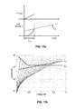
- FIG. 7 a illustrates a current thresholding technique used in the read measurement circuit to generate a time metric for cell-state.
- FIG. 7 b further illustrates a current thresholding technique used in the read measurement circuit to generate a time metric for cell-state
- FIG. 8 compares cell programming curves obtained with the time metric and the conventional low-field resistance metric.
- FIG. 9 a illustrates programming curves for the same cell-state regime with the resistance metric and time metric respectively.
- FIG. 9 b further illustrates programming curves for the same cell-state regime with the resistance metric and time metric respectively.
- FIG. 10 shows the time metric as a function of amorphous thickness.
- FIG. 11 a illustrates a technique for generating a time metric in embodiments of the present invention.
- FIG. 11 b illustrates another technique for generating a time metric in embodiments of the present invention.
- FIG. 12 illustrates a modification to the time metric generation technique of FIGS. 7 a and 7 b.
- FIG. 13 a illustrates a possible modification to the time metric generation technique.
- FIG. 13 b illustrates another possible modification to the time metric generation technique
- FIG. 14 illustrates a further technique for generating a time metric in embodiments of the invention.
- An embodiment of a first aspect of the present invention provides a method for determining the state of a phase-change memory cell.
- the method includes:
- the cell instead of applying a constant read voltage, can be biased with a read voltage which varies with time.
- a measurement is made. This measurement is dependent on a predetermined condition, which depends on the current flowing through the cell, being satisfied. For example, in some embodiments the measurement is indicative of the read voltage level at which the current-dependent condition is satisfied. In other embodiments, the measurement is indicative of the time taken for the current-dependent condition to be satisfied. In any case, the resulting measurement can then be used to determine cell-state.
- the read voltage varies in embodiments of the invention, the cell current varies accordingly in dependence on the I/V characteristic for the cell state in question.
- methods embodying the invention can exploit differences in form of the I/V characteristic for different cell states in a effective manner.
- the resulting measurement provides a good metric for amorphous size (the fundamental programmed entity) and hence for cell-state.
- the metric can be used to probe the high field region of cell operation and can effectively distinguish states with high amorphous fractions. This can increase the available programming space, allowing operation with more levels and hence storage of more bits per cell.
- the metric can also offer the prospect of MLC operation with improved tolerance to drift and low frequency noise.
- the form of the read voltage is predetermined.
- the cell is biased with a predetermined read voltage which varies with time over a range of voltage levels.
- the measurement that is made can be indicative of the time taken for the predetermined condition to be satisfied. This provides a time-based metric for determining cell-state.
- the read voltage does not vary with time in a predetermined manner.
- the measurement that is made can be indicative of the read voltage level at which the predetermined condition is satisfied.
- the read voltage level can be varied in a substantially random manner until the current-dependent condition is determined to be satisfied, the read voltage level at which this occurs being measured in this case. This will be discussed further below.
- the read voltage can vary in an analog or a digital manner.
- the read voltage preferably increases with time.
- the read voltage generally increases with increasing time and, according to further embodiments, the read voltage increases monotonically with time.
- the read voltage can be a linear function of time, or a non-linear function of time, and examples of both cases will be discussed below. While the way in which the read voltage varies with time can be predetermined for the read operation, the duration of application of the read voltage can differ for different read operations. In particular, preferred embodiments include ceasing application of the read voltage when the predetermined condition is satisfied. The duration of the read voltage can therefore vary for different measurements.
- the detection condition discussed further below can be set so that the read voltage range can traverse threshold switching voltages for at least some of the lower levels while still avoiding level switching.
- the measurement indicative of time can be made in various ways and can directly or indirectly indicate the time in question. Some embodiments can measure time itself in some manner. Other embodiments can measure some other parameter indicative of time. For example, where the predetermined read voltage is a linear function of time, the read voltage level at which the predetermined condition is satisfied can be measured as a time indicator. In embodiments where the read voltage is not predetermined, the measurement indicative of read voltage level can similarly measure read voltage per se or any convenient parameter indicative thereof.
- the predetermined condition can depend on cell current in a variety of ways.
- the condition can be that the cell current reaches a predetermined current level (in particular that it equals or traverses a predetermined detection threshold).
- the condition can be that the cell current changes from a first predetermined current level to a second predetermined current level.
- a predetermined current level employed in these examples can or can not be a function of the read voltage. Where such a current level is a function read voltage, various functions having increasing and/or decreasing profile portions across the read voltage range can be employed. Examples of these and other embodiments will be described below.
- This step can use the basic measurement as the cell-state metric, or can derive the final metric by processing the measurement in some way. Possible examples here include some form of averaging process or further processing based on techniques which can be employed in addition to the basic measurement method, e.g. any additional corrective techniques to further enhance read accuracy.
- the cell-state can be determined by comparing a metric dependent on the measurement with one or more reference values indicative of the different cell-states.
- Embodiments of the invention can be applied to two-level PCM cells as well as to multilevel cells. When applied for determining the state of a multilevel cell (i.e.
- preferred methods can include determining the state of the cell by comparing a metric dependent on the measurement with a plurality of reference values indicative of the s levels of the cell.
- the metric here can be the measurement per se or some other metric obtained by processing the measurement as indicated above.
- the reference values can define cell levels in a variety of ways, e.g. in terms of predetermined threshold values defining boundaries for measurement ranges which map to the different cell states.
- An embodiment of a second aspect of the invention provides apparatus for determining the state of a phase-change memory cell.
- the apparatus includes:
- a measurement circuit for biasing the cell with a time-varying read voltage and for making a measurement dependent on a predetermined condition, which condition is dependent on cell current during application of the read voltage, being satisfied;
- a controller for determining the state of the cell in dependence on the measurement.
- a phase-change memory device is provides:
- phase-change memory including a plurality of phase-change memory cells
- the read/write apparatus for reading and writing data in the phase-change memory cells, where the read/write apparatus includes apparatus according to the second aspect of the invention for determining the state of a the memory cell.
- FIG. 1 of the accompanying drawings shows simulated I/V characteristics for sixteen different resistance levels (cell states) based on measurement data obtained from PCM cells.
- the arrow indicates increasing thickness (ua) of the amorphous phase, and the vertical line indicates a typical bias voltage, Vread, for measuring low-field resistance on read-back.
- the I/V curves of the low-field resistance technique tend to merge at low fields as amorphous thickness increases.
- the low-field resistance tends to saturate with increasing amorphous size. This phenomenon, which is due to cell geometry effects, serves to mask increasing size of the amorphous region when using the resistance metric to determine cell state.
- FIG. 2 is a simplified schematic of a phase-change memory device embodying the invention.
- the device 1 includes phase-change memory 2 for storing data in one or more integrated arrays of multilevel PCM cells. Though shown as a single block in the figure, in general memory 2 can include any desired configuration of PCM storage units ranging, for example, from a single chip or die to a plurality of storage banks each containing multiple packages of storage chips. Reading and writing of data to memory 2 is performed by read/write apparatus 3 .
- Apparatus 3 includes data-write and read-measurement circuitry 4 for writing data to the PCM cells and for making cell measurements allowing determination of cell-state and hence readback of stored data.
- Circuitry 4 can address individual PCM cells for write and read purposes by applying appropriate voltage signals to an array of word and bit lines in memory ensemble 2 . This process can be performed in generally known manner except as detailed hereinafter.
- a read/write controller 5 controls operation of apparatus 3 generally and includes functionality for determining cell-state, i.e. level detection, based on measurements made by circuitry 4 .
- the functionality of controller 5 can be implemented in hardware or software or a combination thereof, though use of hardwired logic circuits is generally preferred for reasons of operating speed. Suitable implementations will be apparent to those skilled in the art from the description herein.
- user data input to device 1 is typically subjected to some form of write-processing, such as coding for error-correction purposes, before being supplied as write data to read/write apparatus 3 .
- readback data output by apparatus 3 is generally processed by a read-processing module 7 , e.g. performing codeword detection and error correction operations, to recover the original input user data.
- modules 6 and 7 are independent of the cell-state metric system to be described and need not be discussed in detail here.
- Each of the multilevel cells in memory 2 can be set to one of s resistance levels, where s>2, corresponding to different amorphous/crystalline states of the cell.
- the resistance values corresponding to the different levels are usually unequally-spaced, typically lying in the log domain.
- circuitry 4 applies a voltage pulse to set the cell to the state corresponding to the appropriate level.
- FIG. 3 illustrates how cell resistance varies with applied voltage for PCM cells. This figure shows an average programming curve (starting from the “set” state (state of maximum crystallization)) for an array of PCM cells as the logarithm of (average) cell resistance R obtained for applied voltage pulses of increasing amplitude V prog .
- the resistance levels corresponding to different programmable cell-states are predefined for MLC operation.
- four levels are indicated by the horizontal lines in this figure, together with the associated write-pulse amplitudes V prog , such as can be defined for four-level PCM operation providing two bits of storage per cell.
- Reading a memory cell involves determining the state of the cell, i.e. detecting which of the predefined levels the cell is set to.
- the device 1 of FIG. 2 employs a method for determining cell-state based on an improved metric for the fundamental programmed entity, namely amorphous size, in PCM cells.
- FIG. 4 is a schematic illustration of a typical PCM cell 10 .
- the cell consists of a layer 11 of phase change material, e.g. Germanium Antimony Telluride (GST), sandwiched between a bottom electrode 12 and a top electrode 13 .
- Top electrode 13 is connected to a bit line BL of the memory cell array.
- the bottom electrode 12 has a radius r of approximately 20 nm and is produced using sub-lithographic means.
- a transistor 14 is typically used as the access device, the gate contact of this transistor being connected to a word line WL of the array.
- the amorphous region 15 can be created within the crystalline GST as described earlier by application of a voltage pulse at the bit line BL or the word line WL.
- the technique is known as voltage-mode programming and the transistor serves as a selection device.
- the technique is known as current-mode programming and the transistor acts as a voltage controlled current source.
- the size of the resulting amorphous region indicated in the figure by amorphous thickness u a , depends on the amplitude of the programming pulse as already described.
- a measurement is performed which provides a metric for this amorphous size, and hence for cell-state. The read operation will now be described with reference to FIGS. 5 to 7 b.
- FIG. 5 is a schematic block diagram of an exemplary read measurement circuit 20 for use in circuitry 4 of the memory device 1 .
- the measurement circuit 20 includes a counter 21 , a digital-to-analog converter (DAC) 22 , a voltage regulator 23 , a current detector 24 and a comparator 25 connected as shown in the figure.
- DAC digital-to-analog converter
- These circuit components can be implemented in any convenient manner using digital or analog circuitry, and suitable implementations will be readily apparent to those skilled in the art.
- the read measurement circuit 20 is shown connected to a PCM cell 10 , represented as a variable resistance in the figure, for a read operation.
- counter 21 initiates a time count, incrementing the count in response to periodic timing signals from controller 5 of the read/write apparatus.
- the count is supplied to DAC 22 whereby the voltage at the output of the DAC increases in fixed steps as the time count is successively incremented.
- This voltage is smoothed by voltage regulator 23 and applied as a bias voltage Vread to the bit line of PCM cell 10 .
- the effect of components 21 to 23 is thus to generate a predetermined read voltage which increases over a range of voltage levels as the time count is successively incremented.
- the read voltage increases monotonically, as a linear function of time, as illustrated schematically in FIG. 6 (where the step-function is represented by a straight line for simplicity).
- the current flowing through cell 10 during application of the read voltage is measured by current detector 24 .
- the detected current level I is output by detector 24 to one input of comparator 25 .
- Comparator 25 compares the current level I with a predetermined current threshold I D . If I ⁇ I D the comparator outputs a control signal to timer 21 which terminates the time count, whereupon application of the read voltage ceases.
- the count value on termination of the time count provides a direct measure of the time taken for the cell current to reach the threshold I D . This count value is supplied as a time metric T M to controller 5 of device 1 , and the cell measurement is complete.
- FIGS. 7 a and 7 b illustrate operation of this embodiment in more detail.
- FIG. 7 a indicates how cell current varies with time up to current threshold I D during read voltage application.
- the current threshold I D is set to a constant value which is selected to be less than the threshold switching current I TH for all cell states.
- FIG. 7 b indicates this current threshold I D for the simulated I/V curves for 16-level cells shown in FIG. 1 . Since read voltage is linear with time in this embodiment, the voltage scale in FIG. 7 b is analogous to time and the voltage at which each curve reaches current threshold I D is a direct analog of the time metric T M measured by circuit 20 .
- Determination of cell state is performed by controller 5 of memory device 1 .
- the metric T M output by measurement circuit 20 is supplied to controller 5 as described above.
- the metric T M is used directly by controller 5 to detect the programmed cell level.
- Level detection can be performed in controller 5 simply by comparing the metric T M with a plurality of predetermined reference values.
- the reference values can correspond, for example, to pre-calculated metric values defining the different cell levels, or threshold values defining the boundaries between respective ranges of metric values which are deemed to map to the different cell levels. Comparison of the calculated metric with the reference values in controller 5 thus yields the stored cell-level.
- the resulting readback data is then output by controller 5 for further read-processing in order to recover the user data as discussed above.
- the metric T M has very considerable advantages over the conventional low-field resistance metric. As already illustrated by FIG. 7 b , the geometric effects which limit performance of the resistance metric do not significantly impact the metric T M . The metric T M can therefore effectively capture high-u a cell states. The technique described also allows the metric T M to probe the high-field region without danger of disturbing cell-state (level-switching). As a consequence of these features, the usable programming space can be significantly enhanced when the metric T M is used to determine cell-state. This is apparent from FIG. 8 which compares average programming curves measured with the resistance metric (logR) and the metric T M normalized to the same effective window.
- logR resistance metric
- FIG. 9 a shows the programming curve for four-level PCM cells using the resistance metric to measure the programmed state.
- FIG. 9 b shows the equivalent curve using the metric T M in the same cell-state regime.
- the ordinate axis here indicates T M in terms of the count value (number of voltage steps) obtained in the FIG. 5 circuit described above. The four cell levels are indicated at L 1 to L 4 in the figures.
- FIG. 9 b shows that the metric T M provides two more usable programmable levels than the resistance metric in this scenario.
- time metric T M of the above embodiment can be expressed as:
- T M 2 ⁇ ⁇ kTu aeff q ⁇ ⁇ ⁇ ⁇ ⁇ zk slope ⁇ sinh - 1 [ I D ⁇ ⁇ 0 ⁇ ⁇ ⁇ ⁇ z 2 ⁇ e E c - E f k ⁇ ⁇ T 2 ⁇ q ⁇ ⁇ ⁇ ⁇ ⁇ r eff ] ( 3 )
- the resistance metric is a strong function of the activation energy of the cell.
- the activation energy is strongly influenced by the defect density and physical attributes like compressive and tensile stress. Drift behaviour commonly observed in the resistance metric, and low frequency fluctuations, are attributed to similar variations in activation energy. However, it can be seen that these undesirable attributes are not related to the fundamental programmed entity which is the amorphous size and the corresponding effective amorphous thickness.
- the metric T M is a strong function of the effective amorphous thickness but is less dependent on the activation energy.
- the resistance metric is proportional to the activation energy term in equation (2), this term only appears in the 1/sin h term in equation (3) for the metric T M . This indicates a significant reduction in impact of drift and low frequency noise on the metric T M .
- Equation (3) also indicates that the time metric is a strong function of the effective amorphous thickness but only a weak function of the effective contact radius r eff . This indicates that the time metric should not saturate at high values of amorphous thickness as already discussed above. This is further confirmed by the plot of T M against amorphous thickness obtained from simulation results in FIG. 10 . This shows strong linearity of T M with amorphous thickness and good level discrimination across the range.
- a still further advantage over the resistance metric is that the metric T M is directly measured and so there is no 1/x compression. Overall, therefore, it will be seen that the metric T M provides an improved metric for amorphous size and hence cell-state.
- FIGS. 11 a and 11 b illustrate a first alternative method using figures of similar form to FIGS. 7 a and 7 b .
- the condition to be satisfied by the cell current on making the time measurement is different to that of the first embodiment.
- the condition here is that the cell current I changes from a first, lower current level I D1 to a second, higher current level I D2 .
- the time for the cell current to increase from the lower to the higher threshold is measured as the metric T M .
- T M The time for the cell current to increase from the lower to the higher threshold is measured as the metric T M .
- Equation (3) indicates that this “time difference metric” can exhibit even greater tolerance to drift and low frequency noise.
- FIG. 12 illustrates a modification to the FIG. 7 a technique in which the bias voltage V read is a non-linear function of time.
- the voltage ramp can be tailored to correct for the hyperbolic sine behavior which causes deviation of the time metric from exponential form at low voltages.
- Non-linearity can also be used to increase the read bandwidth and/or increase margin of the metric.
- the time dependence of the read voltage can be altered in various ways to achieve desired effects in different embodiments.
- the current thresholds used in the foregoing embodiments are independent of the read voltage V read .
- Alternative embodiments can use current thresholds which are functions of the read voltage.
- the predetermined current level can be the threshold switching current. This varies with level, tending to be higher at low levels of amorphous thickness.
- the read voltage can be increased until the cell current reaches the switching threshold for the level in question, and the measurement circuit can record the time at which the cell switches.
- Randomness in the switching threshold can also limit accuracy in this case. In general, therefore, it can be preferred that any current threshold is defined so as to avoid level switching.
- this can be done by ensuring that the threshold level at any read voltage level is less than the threshold switching current for all cell states. In other embodiments, however, the threshold can vary with read voltage so as to stay under potential switching thresholds attainable at any given voltage level but not necessarily under switching thresholds for all states, in particular those which switch at higher voltage levels. In these embodiments, at any read voltage level, the threshold current level should be less than the threshold switching current for any cell states having a threshold switching voltage up to that read voltage level.
- FIGS. 13 a and 13 b illustrate two examples of current thresholds which are functions of the read voltage.
- threshold I D1 the current threshold is higher at high voltages to increase the signal-to-noise ratio (SNR) in the high-field regime.
- threshold I D2 the current threshold is higher at low voltages to increase resolution in the low-field regime.
- This threshold illustrates how the threshold level at a given read voltage level can be higher than the threshold switching current for cell states having threshold switching voltages above that read voltage level).
- the threshold switching current is significantly higher.
- an increased current threshold I D2 at low voltage levels can be employed to enhance the SNR.
- I D2 is still low enough to avoid switching of levels corresponding to high amorphous thickness.
- FIG. 14 illustrates an alternative embodiment in which the condition to be satisfied for the time measurement is that a parameter dependent on an integral of the cell current reaches a predetermined level.
- this threshold level can be set appropriately to avoid threshold switching.
- a constant threshold voltage level V D is used although the threshold can be made dependent on read voltage if desired.
- Other parameters dependent on the cell current can also be monitored in other embodiments.
- time measurement T M is used directly as the metric for discriminating levels above, if desired the time measurement can be subjected to further processing (e.g. based on additional corrective techniques) to derive the final cell-state metric.
- another parameter indicative of time can be measured, e.g. read voltage level in some embodiments.
- the predetermined read voltage is a monotonically increasing function as in the embodiments described, alternatives can be envisaged in which the voltage increases generally, though not monotonically, or even decreases with time.
- an embodiment can be envisaged using a time difference metric similar to FIG. 11 a in which the read voltage is ramped down from a predetermined (sub-switching threshold) level and the cell current decreases from a higher to a lower threshold.
- the read voltage scan is stopped when the time measurement is taken. While this can be preferred for the reasons already discussed, it need not necessarily be so. For example, if the read voltage is always scanned through the entire voltage range, regardless of measurement completion, a cell whose state is then altered after detection can be immediately re-programmed.
- Our European patent application filed concurrently herewith under Applicant's reference CH9-2010-0093 discloses a technique exploiting methods of this type for use in programming cell states.
- the read voltage varies with time in a predetermined manner and the cell-state metric is based on a measurement of the time taken for a condition dependent on cell current to be satisfied.
- Alternative embodiments can be envisaged however.
- embodiments of the present invention can be envisaged in which the read voltage does not vary with time in a predetermined manner.
- the read voltage can be varied in a substantially random manner until the current-dependent condition is determined to be satisfied.
- a (possibly arbitrary) read voltage level can be selected as a starting point, and this level can then be varied according to some predefined algorithm until the current-dependent condition is determined to be satisfied.
- a particular example here can be to vary the read voltage in a feedback manner.
- the subsequent read voltage levels can be determined based on cell current.
- the read voltage level can thus be caused gradually to converge on the particular level at which the current-dependent condition is satisfied.
- the measurement used as a metric for cell-state can be a measurement which is (directly or indirectly) indicative of the read voltage level at which the current-dependent condition is satisfied.
- Such a metric is superior to the conventional resistance metric for equivalent reasons to those discussed above in connection with the time metric.
Abstract
Description
Claims (15)
Priority Applications (1)
| Application Number | Priority Date | Filing Date | Title |
|---|---|---|---|
| US13/573,000 US8780611B2 (en) | 2011-03-10 | 2012-08-13 | Determining cell-state in phase-change memory |
Applications Claiming Priority (3)
| Application Number | Priority Date | Filing Date | Title |
|---|---|---|---|
| EP11157698.9 | 2011-03-10 | ||
| EP11157698 | 2011-03-10 | ||
| EP11157698 | 2011-03-10 |
Related Child Applications (1)
| Application Number | Title | Priority Date | Filing Date |
|---|---|---|---|
| US13/573,000 Continuation US8780611B2 (en) | 2011-03-10 | 2012-08-13 | Determining cell-state in phase-change memory |
Publications (2)
| Publication Number | Publication Date |
|---|---|
| US20120230097A1 US20120230097A1 (en) | 2012-09-13 |
| US8755214B2 true US8755214B2 (en) | 2014-06-17 |
Family
ID=46795462
Family Applications (2)
| Application Number | Title | Priority Date | Filing Date |
|---|---|---|---|
| US13/415,012 Active 2032-08-03 US8755214B2 (en) | 2011-03-10 | 2012-03-08 | Determining cell-state in phase-change memory |
| US13/573,000 Active US8780611B2 (en) | 2011-03-10 | 2012-08-13 | Determining cell-state in phase-change memory |
Family Applications After (1)
| Application Number | Title | Priority Date | Filing Date |
|---|---|---|---|
| US13/573,000 Active US8780611B2 (en) | 2011-03-10 | 2012-08-13 | Determining cell-state in phase-change memory |
Country Status (4)
| Country | Link |
|---|---|
| US (2) | US8755214B2 (en) |
| EP (1) | EP2684193B1 (en) |
| CN (1) | CN103415889B (en) |
| WO (1) | WO2012120401A1 (en) |
Cited By (5)
| Publication number | Priority date | Publication date | Assignee | Title |
|---|---|---|---|---|
| US9047179B2 (en) * | 2012-08-29 | 2015-06-02 | International Business Machines Corporation | Level placement in solid-state memory |
| US9343148B2 (en) | 2014-03-26 | 2016-05-17 | International Business Machines Corporation | Method and apparatus for faster determination of a cell state of a resistive memory cell using a parallel resistor |
| US9666273B2 (en) | 2015-06-18 | 2017-05-30 | International Business Machines Corporation | Determining a cell state of a resistive memory cell |
| TWI595334B (en) * | 2015-08-03 | 2017-08-11 | 旺宏電子股份有限公司 | Timing device and method thereof |
| US9972387B2 (en) | 2014-10-31 | 2018-05-15 | Hewlett Packard Enterprise Development Lp | Sensing circuit for resistive memory |
Families Citing this family (7)
| Publication number | Priority date | Publication date | Assignee | Title |
|---|---|---|---|---|
| GB2502553A (en) * | 2012-05-30 | 2013-12-04 | Ibm | Read measurements of resistive memory cells |
| GB2510339A (en) * | 2013-01-30 | 2014-08-06 | Ibm | Method and apparatus for read measurement of a plurality of resistive memory cells |
| GB2518632A (en) * | 2013-09-26 | 2015-04-01 | Ibm | Estimation of level-thresholds for memory cells |
| US9520189B1 (en) | 2015-10-29 | 2016-12-13 | International Business Machines Corporation | Enhanced temperature compensation for resistive memory cell circuits |
| KR102619682B1 (en) * | 2016-12-13 | 2023-12-28 | 삼성전자주식회사 | Memory device and method for operating memory device |
| US11501826B2 (en) | 2017-10-17 | 2022-11-15 | R&D3 Llc | Memory device having variable impedance memory cells and time-to-transition sensing of data stored therein |
| US10269413B1 (en) | 2017-10-17 | 2019-04-23 | R&D 3 Llc | Memory device having variable impedance memory cells and time-to-transition sensing of data stored therein |
Citations (15)
| Publication number | Priority date | Publication date | Assignee | Title |
|---|---|---|---|---|
| US20030043631A1 (en) * | 2001-08-30 | 2003-03-06 | Gilton Terry L. | Method of retaining memory state in a programmable conductor RAM |
| CN1628357A (en) | 2002-08-14 | 2005-06-15 | 英特尔公司 | Method for reading structural phase-Change memory |
| US20060023497A1 (en) | 2004-07-28 | 2006-02-02 | Sharp Kabushiki Kaisha | Nonvolatile semiconductor memory device and read method |
| CN1747058A (en) | 2004-06-19 | 2006-03-15 | 三星电子株式会社 | Adopt the phase-change memory device and the control method thereof of Control current method |
| US7247547B2 (en) | 2005-01-05 | 2007-07-24 | International Business Machines Corporation | Method of fabricating a field effect transistor having improved junctions |
| CN101236779A (en) | 2007-01-31 | 2008-08-06 | 旺宏电子股份有限公司 | Storage device and its programming method |
| US7505334B1 (en) | 2008-05-28 | 2009-03-17 | International Business Machines Corporation | Measurement method for reading multi-level memory cell utilizing measurement time delay as the characteristic parameter for level definition |
| KR100895400B1 (en) | 2007-12-03 | 2009-05-06 | 주식회사 하이닉스반도체 | Phase change memory device |
| US7573775B2 (en) | 2006-02-09 | 2009-08-11 | Fujitsu Limited | Setting threshold voltages of cells in a memory block to reduce leakage in the memory block |
| US7646633B2 (en) | 2007-03-02 | 2010-01-12 | Elpida Memory, Inc. | Method for programming phase-change memory and method for reading date from the same |
| US20100259993A1 (en) * | 2009-04-09 | 2010-10-14 | Samsung Electronics Co., Ltd. | Semiconductor memory device and related method of programming |
| US20110051497A1 (en) | 2009-09-02 | 2011-03-03 | Samsung Electronics Co., Ltd. | Method of measuring a resistance of a resistive memory device |
| US7986549B1 (en) * | 2008-12-29 | 2011-07-26 | Micron Technology, Inc. | Apparatus and method for refreshing or toggling a phase-change memory cell |
| US20120069633A1 (en) | 2010-03-30 | 2012-03-22 | Yoshikazu Katoh | Nonvolatile storage device and method for writing into the same |
| US20130063997A1 (en) * | 2011-09-14 | 2013-03-14 | Ariel Maislos | High-Resolution Readout of Analog Memory Cells |
Family Cites Families (2)
| Publication number | Priority date | Publication date | Assignee | Title |
|---|---|---|---|---|
| EP1699054A1 (en) * | 2005-03-03 | 2006-09-06 | STMicroelectronics S.r.l. | A memory device with a ramp-like voltage biasing structure and reduced number of reference cells |
| US7929338B2 (en) * | 2009-02-24 | 2011-04-19 | International Business Machines Corporation | Memory reading method for resistance drift mitigation |
-
2012
- 2012-02-24 CN CN201280012580.5A patent/CN103415889B/en not_active Expired - Fee Related
- 2012-02-24 EP EP12755289.1A patent/EP2684193B1/en active Active
- 2012-02-24 WO PCT/IB2012/050848 patent/WO2012120401A1/en active Application Filing
- 2012-03-08 US US13/415,012 patent/US8755214B2/en active Active
- 2012-08-13 US US13/573,000 patent/US8780611B2/en active Active
Patent Citations (15)
| Publication number | Priority date | Publication date | Assignee | Title |
|---|---|---|---|---|
| US20030043631A1 (en) * | 2001-08-30 | 2003-03-06 | Gilton Terry L. | Method of retaining memory state in a programmable conductor RAM |
| CN1628357A (en) | 2002-08-14 | 2005-06-15 | 英特尔公司 | Method for reading structural phase-Change memory |
| CN1747058A (en) | 2004-06-19 | 2006-03-15 | 三星电子株式会社 | Adopt the phase-change memory device and the control method thereof of Control current method |
| US20060023497A1 (en) | 2004-07-28 | 2006-02-02 | Sharp Kabushiki Kaisha | Nonvolatile semiconductor memory device and read method |
| US7247547B2 (en) | 2005-01-05 | 2007-07-24 | International Business Machines Corporation | Method of fabricating a field effect transistor having improved junctions |
| US7573775B2 (en) | 2006-02-09 | 2009-08-11 | Fujitsu Limited | Setting threshold voltages of cells in a memory block to reduce leakage in the memory block |
| CN101236779A (en) | 2007-01-31 | 2008-08-06 | 旺宏电子股份有限公司 | Storage device and its programming method |
| US7646633B2 (en) | 2007-03-02 | 2010-01-12 | Elpida Memory, Inc. | Method for programming phase-change memory and method for reading date from the same |
| KR100895400B1 (en) | 2007-12-03 | 2009-05-06 | 주식회사 하이닉스반도체 | Phase change memory device |
| US7505334B1 (en) | 2008-05-28 | 2009-03-17 | International Business Machines Corporation | Measurement method for reading multi-level memory cell utilizing measurement time delay as the characteristic parameter for level definition |
| US7986549B1 (en) * | 2008-12-29 | 2011-07-26 | Micron Technology, Inc. | Apparatus and method for refreshing or toggling a phase-change memory cell |
| US20100259993A1 (en) * | 2009-04-09 | 2010-10-14 | Samsung Electronics Co., Ltd. | Semiconductor memory device and related method of programming |
| US20110051497A1 (en) | 2009-09-02 | 2011-03-03 | Samsung Electronics Co., Ltd. | Method of measuring a resistance of a resistive memory device |
| US20120069633A1 (en) | 2010-03-30 | 2012-03-22 | Yoshikazu Katoh | Nonvolatile storage device and method for writing into the same |
| US20130063997A1 (en) * | 2011-09-14 | 2013-03-14 | Ariel Maislos | High-Resolution Readout of Analog Memory Cells |
Non-Patent Citations (3)
| Title |
|---|
| Bhaskaran, H. et al. "Method of Fabricating a Semiconductor Device" Final Office Action for U.S. Appl. No. 13/083,057 as mail on Aug. 21, 2013. (12 Pages). |
| Frey, U., et al. "Determining Cell-State in Phase-Change Memory". Non Final Office Action for U.S. Appl. No. 13/573,000 mailed on Oct. 24, 2013. (13 Pages). |
| Patent Cooperation Treaty, "Notification of Transmittal of the International Search Report and the Written Opinion of the International Searching Authority, or the Declaration" Issued for PCT/IB2012/050848 on Jul. 12, 2012. (9 Pages). |
Cited By (9)
| Publication number | Priority date | Publication date | Assignee | Title |
|---|---|---|---|---|
| US9047179B2 (en) * | 2012-08-29 | 2015-06-02 | International Business Machines Corporation | Level placement in solid-state memory |
| US9256375B2 (en) * | 2012-08-29 | 2016-02-09 | International Business Machines Corporation | Level placement in solid-state memory |
| US9343148B2 (en) | 2014-03-26 | 2016-05-17 | International Business Machines Corporation | Method and apparatus for faster determination of a cell state of a resistive memory cell using a parallel resistor |
| US9496031B2 (en) | 2014-03-26 | 2016-11-15 | International Business Machines Corporation | Method and apparatus for faster determination of a cell state of a resistive memory cell using a parallel resistor |
| US9953706B2 (en) | 2014-03-26 | 2018-04-24 | International Business Machines Corporation | Method and apparatus for faster determination of cell state of a resistive memory cell using a parallel resistor |
| US9972387B2 (en) | 2014-10-31 | 2018-05-15 | Hewlett Packard Enterprise Development Lp | Sensing circuit for resistive memory |
| US9666273B2 (en) | 2015-06-18 | 2017-05-30 | International Business Machines Corporation | Determining a cell state of a resistive memory cell |
| US10395734B2 (en) | 2015-06-18 | 2019-08-27 | International Business Machines Corporation | Method and apparatus for determining a cell state of a resistive memory cell |
| TWI595334B (en) * | 2015-08-03 | 2017-08-11 | 旺宏電子股份有限公司 | Timing device and method thereof |
Also Published As
| Publication number | Publication date |
|---|---|
| US20120230097A1 (en) | 2012-09-13 |
| CN103415889B (en) | 2017-02-15 |
| EP2684193B1 (en) | 2019-08-14 |
| EP2684193A4 (en) | 2014-11-05 |
| US8780611B2 (en) | 2014-07-15 |
| CN103415889A (en) | 2013-11-27 |
| EP2684193A1 (en) | 2014-01-15 |
| US20120307554A1 (en) | 2012-12-06 |
| WO2012120401A1 (en) | 2012-09-13 |
Similar Documents
| Publication | Publication Date | Title |
|---|---|---|
| US8755214B2 (en) | Determining cell-state in phase-change memory | |
| US20120230081A1 (en) | Cell-state measurement in resistive memory | |
| US9269435B2 (en) | Drift mitigation for multi-bits phase change memory | |
| US9293198B2 (en) | Programming of gated phase-change memory cells | |
| CN102422361B (en) | Non-volatile storage device and method for writing to non-volatile storage device | |
| CN110036444B (en) | Adaptive memory cell write conditions | |
| US8009455B2 (en) | Programmable resistance memory | |
| US9070438B2 (en) | Programming of phase-change memory cells | |
| KR20140024304A (en) | Conditional programming of multibit memory cells | |
| Le et al. | RADAR: A fast and energy-efficient programming technique for multiple bits-per-cell RRAM arrays | |
| US9343148B2 (en) | Method and apparatus for faster determination of a cell state of a resistive memory cell using a parallel resistor | |
| US9236120B2 (en) | Read measurement of resistive memory cells | |
| US20120327709A1 (en) | Programming of phase-change memory cells | |
| JP5705321B2 (en) | Method and apparatus for determining the state of a phase change memory cell | |
| US9076517B2 (en) | Memory apparatus with gated phase-change memory cells | |
| CN109410997B (en) | Resistive memory storage device and writing method thereof | |
| Bits-Per-Cell | RADAR: A Fast and Energy-Efficient Programming Technique for Multiple | |
| US20150302921A1 (en) | Device and method for determining a cell level of a resistive memory cell |
Legal Events
| Date | Code | Title | Description |
|---|---|---|---|
| AS | Assignment |
Owner name: INTERNATIONAL BUSINESS MACHINES CORPORATION, NEW Y Free format text: ASSIGNMENT OF ASSIGNORS INTEREST;ASSIGNORS:FREY, URS;PANTAZI, ANGELIKI;PAPANDREOU, NIKOLAOS;AND OTHERS;REEL/FRAME:027826/0557 Effective date: 20120306 |
|
| STCF | Information on status: patent grant |
Free format text: PATENTED CASE |
|
| AS | Assignment |
Owner name: GLOBALFOUNDRIES U.S. 2 LLC, NEW YORK Free format text: ASSIGNMENT OF ASSIGNORS INTEREST;ASSIGNOR:INTERNATIONAL BUSINESS MACHINES CORPORATION;REEL/FRAME:036550/0001 Effective date: 20150629 |
|
| AS | Assignment |
Owner name: GLOBALFOUNDRIES INC., CAYMAN ISLANDS Free format text: ASSIGNMENT OF ASSIGNORS INTEREST;ASSIGNORS:GLOBALFOUNDRIES U.S. 2 LLC;GLOBALFOUNDRIES U.S. INC.;REEL/FRAME:036779/0001 Effective date: 20150910 |
|
| MAFP | Maintenance fee payment |
Free format text: PAYMENT OF MAINTENANCE FEE, 4TH YEAR, LARGE ENTITY (ORIGINAL EVENT CODE: M1551) Year of fee payment: 4 |
|
| AS | Assignment |
Owner name: WILMINGTON TRUST, NATIONAL ASSOCIATION, DELAWARE Free format text: SECURITY AGREEMENT;ASSIGNOR:GLOBALFOUNDRIES INC.;REEL/FRAME:049490/0001 Effective date: 20181127 |
|
| AS | Assignment |
Owner name: GLOBALFOUNDRIES U.S. INC., CALIFORNIA Free format text: ASSIGNMENT OF ASSIGNORS INTEREST;ASSIGNOR:GLOBALFOUNDRIES INC.;REEL/FRAME:054633/0001 Effective date: 20201022 |
|
| AS | Assignment |
Owner name: GLOBALFOUNDRIES INC., CAYMAN ISLANDS Free format text: RELEASE BY SECURED PARTY;ASSIGNOR:WILMINGTON TRUST, NATIONAL ASSOCIATION;REEL/FRAME:054636/0001 Effective date: 20201117 |
|
| AS | Assignment |
Owner name: GLOBALFOUNDRIES U.S. INC., NEW YORK Free format text: RELEASE BY SECURED PARTY;ASSIGNOR:WILMINGTON TRUST, NATIONAL ASSOCIATION;REEL/FRAME:056987/0001 Effective date: 20201117 |
|
| MAFP | Maintenance fee payment |
Free format text: PAYMENT OF MAINTENANCE FEE, 8TH YEAR, LARGE ENTITY (ORIGINAL EVENT CODE: M1552); ENTITY STATUS OF PATENT OWNER: LARGE ENTITY Year of fee payment: 8 |