US8772929B2 - Package for three dimensional integrated circuit - Google Patents
Package for three dimensional integrated circuit Download PDFInfo
- Publication number
- US8772929B2 US8772929B2 US13/297,992 US201113297992A US8772929B2 US 8772929 B2 US8772929 B2 US 8772929B2 US 201113297992 A US201113297992 A US 201113297992A US 8772929 B2 US8772929 B2 US 8772929B2
- Authority
- US
- United States
- Prior art keywords
- recess
- semiconductor die
- wafer
- semiconductor
- recess portion
- Prior art date
- Legal status (The legal status is an assumption and is not a legal conclusion. Google has not performed a legal analysis and makes no representation as to the accuracy of the status listed.)
- Active
Links
- 239000004065 semiconductor Substances 0.000 claims abstract description 109
- 239000000758 substrate Substances 0.000 claims abstract description 32
- 238000002955 isolation Methods 0.000 claims description 15
- 150000001875 compounds Chemical class 0.000 claims description 8
- 239000002184 metal Substances 0.000 claims description 6
- 238000000034 method Methods 0.000 abstract description 57
- 230000008569 process Effects 0.000 abstract description 46
- 238000004519 manufacturing process Methods 0.000 abstract description 9
- 235000012431 wafers Nutrition 0.000 description 71
- 239000010410 layer Substances 0.000 description 38
- 239000000463 material Substances 0.000 description 17
- 238000000227 grinding Methods 0.000 description 7
- 238000000465 moulding Methods 0.000 description 6
- 239000004593 Epoxy Substances 0.000 description 4
- 230000008901 benefit Effects 0.000 description 4
- 238000005516 engineering process Methods 0.000 description 3
- 230000006870 function Effects 0.000 description 3
- 239000000203 mixture Substances 0.000 description 3
- 239000004642 Polyimide Substances 0.000 description 2
- 239000003990 capacitor Substances 0.000 description 2
- 238000005229 chemical vapour deposition Methods 0.000 description 2
- 238000000576 coating method Methods 0.000 description 2
- 238000005336 cracking Methods 0.000 description 2
- 238000009792 diffusion process Methods 0.000 description 2
- 230000006872 improvement Effects 0.000 description 2
- 230000010354 integration Effects 0.000 description 2
- 239000011229 interlayer Substances 0.000 description 2
- 229910044991 metal oxide Inorganic materials 0.000 description 2
- 150000004706 metal oxides Chemical class 0.000 description 2
- 238000004806 packaging method and process Methods 0.000 description 2
- 238000000623 plasma-assisted chemical vapour deposition Methods 0.000 description 2
- 229920001721 polyimide Polymers 0.000 description 2
- 229920000642 polymer Polymers 0.000 description 2
- 239000011347 resin Substances 0.000 description 2
- 229920005989 resin Polymers 0.000 description 2
- 229910000679 solder Inorganic materials 0.000 description 2
- VYPSYNLAJGMNEJ-UHFFFAOYSA-N Silicium dioxide Chemical compound O=[Si]=O VYPSYNLAJGMNEJ-UHFFFAOYSA-N 0.000 description 1
- XUIMIQQOPSSXEZ-UHFFFAOYSA-N Silicon Chemical compound [Si] XUIMIQQOPSSXEZ-UHFFFAOYSA-N 0.000 description 1
- 230000004075 alteration Effects 0.000 description 1
- 238000005452 bending Methods 0.000 description 1
- 229910010293 ceramic material Inorganic materials 0.000 description 1
- 239000003989 dielectric material Substances 0.000 description 1
- 238000009826 distribution Methods 0.000 description 1
- 238000005530 etching Methods 0.000 description 1
- 238000001746 injection moulding Methods 0.000 description 1
- 239000012212 insulator Substances 0.000 description 1
- 238000003475 lamination Methods 0.000 description 1
- 239000007788 liquid Substances 0.000 description 1
- 238000012986 modification Methods 0.000 description 1
- 230000004048 modification Effects 0.000 description 1
- 239000011368 organic material Substances 0.000 description 1
- 230000003071 parasitic effect Effects 0.000 description 1
- 238000007517 polishing process Methods 0.000 description 1
- 229910052710 silicon Inorganic materials 0.000 description 1
- 239000010703 silicon Substances 0.000 description 1
- 229910052814 silicon oxide Inorganic materials 0.000 description 1
- 238000009987 spinning Methods 0.000 description 1
- 239000000126 substance Substances 0.000 description 1
- 238000006467 substitution reaction Methods 0.000 description 1
- 230000008646 thermal stress Effects 0.000 description 1
Images


Classifications
-
- H—ELECTRICITY
- H01—ELECTRIC ELEMENTS
- H01L—SEMICONDUCTOR DEVICES NOT COVERED BY CLASS H10
- H01L24/00—Arrangements for connecting or disconnecting semiconductor or solid-state bodies; Methods or apparatus related thereto
- H01L24/93—Batch processes
- H01L24/95—Batch processes at chip-level, i.e. with connecting carried out on a plurality of singulated devices, i.e. on diced chips
- H01L24/97—Batch processes at chip-level, i.e. with connecting carried out on a plurality of singulated devices, i.e. on diced chips the devices being connected to a common substrate, e.g. interposer, said common substrate being separable into individual assemblies after connecting
-
- H—ELECTRICITY
- H01—ELECTRIC ELEMENTS
- H01L—SEMICONDUCTOR DEVICES NOT COVERED BY CLASS H10
- H01L21/00—Processes or apparatus adapted for the manufacture or treatment of semiconductor or solid state devices or of parts thereof
- H01L21/02—Manufacture or treatment of semiconductor devices or of parts thereof
- H01L21/04—Manufacture or treatment of semiconductor devices or of parts thereof the devices having at least one potential-jump barrier or surface barrier, e.g. PN junction, depletion layer or carrier concentration layer
- H01L21/50—Assembly of semiconductor devices using processes or apparatus not provided for in a single one of the subgroups H01L21/06 - H01L21/326, e.g. sealing of a cap to a base of a container
- H01L21/56—Encapsulations, e.g. encapsulation layers, coatings
- H01L21/563—Encapsulation of active face of flip-chip device, e.g. underfilling or underencapsulation of flip-chip, encapsulation preform on chip or mounting substrate
-
- H—ELECTRICITY
- H01—ELECTRIC ELEMENTS
- H01L—SEMICONDUCTOR DEVICES NOT COVERED BY CLASS H10
- H01L21/00—Processes or apparatus adapted for the manufacture or treatment of semiconductor or solid state devices or of parts thereof
- H01L21/02—Manufacture or treatment of semiconductor devices or of parts thereof
- H01L21/04—Manufacture or treatment of semiconductor devices or of parts thereof the devices having at least one potential-jump barrier or surface barrier, e.g. PN junction, depletion layer or carrier concentration layer
- H01L21/50—Assembly of semiconductor devices using processes or apparatus not provided for in a single one of the subgroups H01L21/06 - H01L21/326, e.g. sealing of a cap to a base of a container
- H01L21/56—Encapsulations, e.g. encapsulation layers, coatings
- H01L21/561—Batch processing
-
- H—ELECTRICITY
- H01—ELECTRIC ELEMENTS
- H01L—SEMICONDUCTOR DEVICES NOT COVERED BY CLASS H10
- H01L21/00—Processes or apparatus adapted for the manufacture or treatment of semiconductor or solid state devices or of parts thereof
- H01L21/70—Manufacture or treatment of devices consisting of a plurality of solid state components formed in or on a common substrate or of parts thereof; Manufacture of integrated circuit devices or of parts thereof
- H01L21/77—Manufacture or treatment of devices consisting of a plurality of solid state components or integrated circuits formed in, or on, a common substrate
- H01L21/78—Manufacture or treatment of devices consisting of a plurality of solid state components or integrated circuits formed in, or on, a common substrate with subsequent division of the substrate into plural individual devices
-
- H—ELECTRICITY
- H01—ELECTRIC ELEMENTS
- H01L—SEMICONDUCTOR DEVICES NOT COVERED BY CLASS H10
- H01L24/00—Arrangements for connecting or disconnecting semiconductor or solid-state bodies; Methods or apparatus related thereto
- H01L24/93—Batch processes
- H01L24/94—Batch processes at wafer-level, i.e. with connecting carried out on a wafer comprising a plurality of undiced individual devices
-
- H—ELECTRICITY
- H01—ELECTRIC ELEMENTS
- H01L—SEMICONDUCTOR DEVICES NOT COVERED BY CLASS H10
- H01L25/00—Assemblies consisting of a plurality of individual semiconductor or other solid state devices ; Multistep manufacturing processes thereof
- H01L25/03—Assemblies consisting of a plurality of individual semiconductor or other solid state devices ; Multistep manufacturing processes thereof all the devices being of a type provided for in the same subgroup of groups H01L27/00 - H01L33/00, or in a single subclass of H10K, H10N, e.g. assemblies of rectifier diodes
- H01L25/04—Assemblies consisting of a plurality of individual semiconductor or other solid state devices ; Multistep manufacturing processes thereof all the devices being of a type provided for in the same subgroup of groups H01L27/00 - H01L33/00, or in a single subclass of H10K, H10N, e.g. assemblies of rectifier diodes the devices not having separate containers
- H01L25/065—Assemblies consisting of a plurality of individual semiconductor or other solid state devices ; Multistep manufacturing processes thereof all the devices being of a type provided for in the same subgroup of groups H01L27/00 - H01L33/00, or in a single subclass of H10K, H10N, e.g. assemblies of rectifier diodes the devices not having separate containers the devices being of a type provided for in group H01L27/00
- H01L25/0652—Assemblies consisting of a plurality of individual semiconductor or other solid state devices ; Multistep manufacturing processes thereof all the devices being of a type provided for in the same subgroup of groups H01L27/00 - H01L33/00, or in a single subclass of H10K, H10N, e.g. assemblies of rectifier diodes the devices not having separate containers the devices being of a type provided for in group H01L27/00 the devices being arranged next and on each other, i.e. mixed assemblies
-
- H—ELECTRICITY
- H01—ELECTRIC ELEMENTS
- H01L—SEMICONDUCTOR DEVICES NOT COVERED BY CLASS H10
- H01L25/00—Assemblies consisting of a plurality of individual semiconductor or other solid state devices ; Multistep manufacturing processes thereof
- H01L25/03—Assemblies consisting of a plurality of individual semiconductor or other solid state devices ; Multistep manufacturing processes thereof all the devices being of a type provided for in the same subgroup of groups H01L27/00 - H01L33/00, or in a single subclass of H10K, H10N, e.g. assemblies of rectifier diodes
- H01L25/04—Assemblies consisting of a plurality of individual semiconductor or other solid state devices ; Multistep manufacturing processes thereof all the devices being of a type provided for in the same subgroup of groups H01L27/00 - H01L33/00, or in a single subclass of H10K, H10N, e.g. assemblies of rectifier diodes the devices not having separate containers
- H01L25/065—Assemblies consisting of a plurality of individual semiconductor or other solid state devices ; Multistep manufacturing processes thereof all the devices being of a type provided for in the same subgroup of groups H01L27/00 - H01L33/00, or in a single subclass of H10K, H10N, e.g. assemblies of rectifier diodes the devices not having separate containers the devices being of a type provided for in group H01L27/00
- H01L25/0657—Stacked arrangements of devices
-
- H—ELECTRICITY
- H01—ELECTRIC ELEMENTS
- H01L—SEMICONDUCTOR DEVICES NOT COVERED BY CLASS H10
- H01L25/00—Assemblies consisting of a plurality of individual semiconductor or other solid state devices ; Multistep manufacturing processes thereof
- H01L25/50—Multistep manufacturing processes of assemblies consisting of devices, each device being of a type provided for in group H01L27/00 or H01L29/00
-
- H—ELECTRICITY
- H01—ELECTRIC ELEMENTS
- H01L—SEMICONDUCTOR DEVICES NOT COVERED BY CLASS H10
- H01L29/00—Semiconductor devices adapted for rectifying, amplifying, oscillating or switching, or capacitors or resistors with at least one potential-jump barrier or surface barrier, e.g. PN junction depletion layer or carrier concentration layer; Details of semiconductor bodies or of electrodes thereof ; Multistep manufacturing processes therefor
- H01L29/02—Semiconductor bodies ; Multistep manufacturing processes therefor
- H01L29/06—Semiconductor bodies ; Multistep manufacturing processes therefor characterised by their shape; characterised by the shapes, relative sizes, or dispositions of the semiconductor regions ; characterised by the concentration or distribution of impurities within semiconductor regions
- H01L29/0657—Semiconductor bodies ; Multistep manufacturing processes therefor characterised by their shape; characterised by the shapes, relative sizes, or dispositions of the semiconductor regions ; characterised by the concentration or distribution of impurities within semiconductor regions characterised by the shape of the body
-
- H—ELECTRICITY
- H01—ELECTRIC ELEMENTS
- H01L—SEMICONDUCTOR DEVICES NOT COVERED BY CLASS H10
- H01L2224/00—Indexing scheme for arrangements for connecting or disconnecting semiconductor or solid-state bodies and methods related thereto as covered by H01L24/00
- H01L2224/01—Means for bonding being attached to, or being formed on, the surface to be connected, e.g. chip-to-package, die-attach, "first-level" interconnects; Manufacturing methods related thereto
- H01L2224/10—Bump connectors; Manufacturing methods related thereto
- H01L2224/12—Structure, shape, material or disposition of the bump connectors prior to the connecting process
- H01L2224/13—Structure, shape, material or disposition of the bump connectors prior to the connecting process of an individual bump connector
- H01L2224/13001—Core members of the bump connector
- H01L2224/13099—Material
- H01L2224/131—Material with a principal constituent of the material being a metal or a metalloid, e.g. boron [B], silicon [Si], germanium [Ge], arsenic [As], antimony [Sb], tellurium [Te] and polonium [Po], and alloys thereof
-
- H—ELECTRICITY
- H01—ELECTRIC ELEMENTS
- H01L—SEMICONDUCTOR DEVICES NOT COVERED BY CLASS H10
- H01L2224/00—Indexing scheme for arrangements for connecting or disconnecting semiconductor or solid-state bodies and methods related thereto as covered by H01L24/00
- H01L2224/01—Means for bonding being attached to, or being formed on, the surface to be connected, e.g. chip-to-package, die-attach, "first-level" interconnects; Manufacturing methods related thereto
- H01L2224/10—Bump connectors; Manufacturing methods related thereto
- H01L2224/15—Structure, shape, material or disposition of the bump connectors after the connecting process
- H01L2224/16—Structure, shape, material or disposition of the bump connectors after the connecting process of an individual bump connector
- H01L2224/161—Disposition
- H01L2224/16151—Disposition the bump connector connecting between a semiconductor or solid-state body and an item not being a semiconductor or solid-state body, e.g. chip-to-substrate, chip-to-passive
- H01L2224/16221—Disposition the bump connector connecting between a semiconductor or solid-state body and an item not being a semiconductor or solid-state body, e.g. chip-to-substrate, chip-to-passive the body and the item being stacked
- H01L2224/16225—Disposition the bump connector connecting between a semiconductor or solid-state body and an item not being a semiconductor or solid-state body, e.g. chip-to-substrate, chip-to-passive the body and the item being stacked the item being non-metallic, e.g. insulating substrate with or without metallisation
-
- H—ELECTRICITY
- H01—ELECTRIC ELEMENTS
- H01L—SEMICONDUCTOR DEVICES NOT COVERED BY CLASS H10
- H01L2224/00—Indexing scheme for arrangements for connecting or disconnecting semiconductor or solid-state bodies and methods related thereto as covered by H01L24/00
- H01L2224/01—Means for bonding being attached to, or being formed on, the surface to be connected, e.g. chip-to-package, die-attach, "first-level" interconnects; Manufacturing methods related thereto
- H01L2224/10—Bump connectors; Manufacturing methods related thereto
- H01L2224/15—Structure, shape, material or disposition of the bump connectors after the connecting process
- H01L2224/17—Structure, shape, material or disposition of the bump connectors after the connecting process of a plurality of bump connectors
- H01L2224/171—Disposition
- H01L2224/1718—Disposition being disposed on at least two different sides of the body, e.g. dual array
- H01L2224/17181—On opposite sides of the body
-
- H—ELECTRICITY
- H01—ELECTRIC ELEMENTS
- H01L—SEMICONDUCTOR DEVICES NOT COVERED BY CLASS H10
- H01L2224/00—Indexing scheme for arrangements for connecting or disconnecting semiconductor or solid-state bodies and methods related thereto as covered by H01L24/00
- H01L2224/01—Means for bonding being attached to, or being formed on, the surface to be connected, e.g. chip-to-package, die-attach, "first-level" interconnects; Manufacturing methods related thereto
- H01L2224/26—Layer connectors, e.g. plate connectors, solder or adhesive layers; Manufacturing methods related thereto
- H01L2224/2612—Auxiliary members for layer connectors, e.g. spacers
- H01L2224/26122—Auxiliary members for layer connectors, e.g. spacers being formed on the semiconductor or solid-state body to be connected
- H01L2224/26145—Flow barriers
-
- H—ELECTRICITY
- H01—ELECTRIC ELEMENTS
- H01L—SEMICONDUCTOR DEVICES NOT COVERED BY CLASS H10
- H01L2224/00—Indexing scheme for arrangements for connecting or disconnecting semiconductor or solid-state bodies and methods related thereto as covered by H01L24/00
- H01L2224/01—Means for bonding being attached to, or being formed on, the surface to be connected, e.g. chip-to-package, die-attach, "first-level" interconnects; Manufacturing methods related thereto
- H01L2224/26—Layer connectors, e.g. plate connectors, solder or adhesive layers; Manufacturing methods related thereto
- H01L2224/28—Structure, shape, material or disposition of the layer connectors prior to the connecting process
- H01L2224/29—Structure, shape, material or disposition of the layer connectors prior to the connecting process of an individual layer connector
- H01L2224/29001—Core members of the layer connector
- H01L2224/29099—Material
- H01L2224/2919—Material with a principal constituent of the material being a polymer, e.g. polyester, phenolic based polymer, epoxy
-
- H—ELECTRICITY
- H01—ELECTRIC ELEMENTS
- H01L—SEMICONDUCTOR DEVICES NOT COVERED BY CLASS H10
- H01L2224/00—Indexing scheme for arrangements for connecting or disconnecting semiconductor or solid-state bodies and methods related thereto as covered by H01L24/00
- H01L2224/01—Means for bonding being attached to, or being formed on, the surface to be connected, e.g. chip-to-package, die-attach, "first-level" interconnects; Manufacturing methods related thereto
- H01L2224/26—Layer connectors, e.g. plate connectors, solder or adhesive layers; Manufacturing methods related thereto
- H01L2224/31—Structure, shape, material or disposition of the layer connectors after the connecting process
- H01L2224/32—Structure, shape, material or disposition of the layer connectors after the connecting process of an individual layer connector
- H01L2224/321—Disposition
- H01L2224/32135—Disposition the layer connector connecting between different semiconductor or solid-state bodies, i.e. chip-to-chip
- H01L2224/32145—Disposition the layer connector connecting between different semiconductor or solid-state bodies, i.e. chip-to-chip the bodies being stacked
-
- H—ELECTRICITY
- H01—ELECTRIC ELEMENTS
- H01L—SEMICONDUCTOR DEVICES NOT COVERED BY CLASS H10
- H01L2224/00—Indexing scheme for arrangements for connecting or disconnecting semiconductor or solid-state bodies and methods related thereto as covered by H01L24/00
- H01L2224/73—Means for bonding being of different types provided for in two or more of groups H01L2224/10, H01L2224/18, H01L2224/26, H01L2224/34, H01L2224/42, H01L2224/50, H01L2224/63, H01L2224/71
- H01L2224/732—Location after the connecting process
- H01L2224/73201—Location after the connecting process on the same surface
- H01L2224/73203—Bump and layer connectors
- H01L2224/73204—Bump and layer connectors the bump connector being embedded into the layer connector
-
- H—ELECTRICITY
- H01—ELECTRIC ELEMENTS
- H01L—SEMICONDUCTOR DEVICES NOT COVERED BY CLASS H10
- H01L2224/00—Indexing scheme for arrangements for connecting or disconnecting semiconductor or solid-state bodies and methods related thereto as covered by H01L24/00
- H01L2224/80—Methods for connecting semiconductor or other solid state bodies using means for bonding being attached to, or being formed on, the surface to be connected
- H01L2224/81—Methods for connecting semiconductor or other solid state bodies using means for bonding being attached to, or being formed on, the surface to be connected using a bump connector
- H01L2224/8119—Arrangement of the bump connectors prior to mounting
- H01L2224/81193—Arrangement of the bump connectors prior to mounting wherein the bump connectors are disposed on both the semiconductor or solid-state body and another item or body to be connected to the semiconductor or solid-state body
-
- H—ELECTRICITY
- H01—ELECTRIC ELEMENTS
- H01L—SEMICONDUCTOR DEVICES NOT COVERED BY CLASS H10
- H01L2224/00—Indexing scheme for arrangements for connecting or disconnecting semiconductor or solid-state bodies and methods related thereto as covered by H01L24/00
- H01L2224/80—Methods for connecting semiconductor or other solid state bodies using means for bonding being attached to, or being formed on, the surface to be connected
- H01L2224/81—Methods for connecting semiconductor or other solid state bodies using means for bonding being attached to, or being formed on, the surface to be connected using a bump connector
- H01L2224/818—Bonding techniques
- H01L2224/81801—Soldering or alloying
- H01L2224/81815—Reflow soldering
-
- H—ELECTRICITY
- H01—ELECTRIC ELEMENTS
- H01L—SEMICONDUCTOR DEVICES NOT COVERED BY CLASS H10
- H01L2224/00—Indexing scheme for arrangements for connecting or disconnecting semiconductor or solid-state bodies and methods related thereto as covered by H01L24/00
- H01L2224/80—Methods for connecting semiconductor or other solid state bodies using means for bonding being attached to, or being formed on, the surface to be connected
- H01L2224/83—Methods for connecting semiconductor or other solid state bodies using means for bonding being attached to, or being formed on, the surface to be connected using a layer connector
- H01L2224/831—Methods for connecting semiconductor or other solid state bodies using means for bonding being attached to, or being formed on, the surface to be connected using a layer connector the layer connector being supplied to the parts to be connected in the bonding apparatus
- H01L2224/83104—Methods for connecting semiconductor or other solid state bodies using means for bonding being attached to, or being formed on, the surface to be connected using a layer connector the layer connector being supplied to the parts to be connected in the bonding apparatus by applying pressure, e.g. by injection
-
- H—ELECTRICITY
- H01—ELECTRIC ELEMENTS
- H01L—SEMICONDUCTOR DEVICES NOT COVERED BY CLASS H10
- H01L2224/00—Indexing scheme for arrangements for connecting or disconnecting semiconductor or solid-state bodies and methods related thereto as covered by H01L24/00
- H01L2224/91—Methods for connecting semiconductor or solid state bodies including different methods provided for in two or more of groups H01L2224/80 - H01L2224/90
- H01L2224/92—Specific sequence of method steps
- H01L2224/9202—Forming additional connectors after the connecting process
-
- H—ELECTRICITY
- H01—ELECTRIC ELEMENTS
- H01L—SEMICONDUCTOR DEVICES NOT COVERED BY CLASS H10
- H01L2224/00—Indexing scheme for arrangements for connecting or disconnecting semiconductor or solid-state bodies and methods related thereto as covered by H01L24/00
- H01L2224/91—Methods for connecting semiconductor or solid state bodies including different methods provided for in two or more of groups H01L2224/80 - H01L2224/90
- H01L2224/92—Specific sequence of method steps
- H01L2224/921—Connecting a surface with connectors of different types
- H01L2224/9212—Sequential connecting processes
- H01L2224/92122—Sequential connecting processes the first connecting process involving a bump connector
- H01L2224/92125—Sequential connecting processes the first connecting process involving a bump connector the second connecting process involving a layer connector
-
- H—ELECTRICITY
- H01—ELECTRIC ELEMENTS
- H01L—SEMICONDUCTOR DEVICES NOT COVERED BY CLASS H10
- H01L2224/00—Indexing scheme for arrangements for connecting or disconnecting semiconductor or solid-state bodies and methods related thereto as covered by H01L24/00
- H01L2224/93—Batch processes
- H01L2224/94—Batch processes at wafer-level, i.e. with connecting carried out on a wafer comprising a plurality of undiced individual devices
-
- H—ELECTRICITY
- H01—ELECTRIC ELEMENTS
- H01L—SEMICONDUCTOR DEVICES NOT COVERED BY CLASS H10
- H01L2224/00—Indexing scheme for arrangements for connecting or disconnecting semiconductor or solid-state bodies and methods related thereto as covered by H01L24/00
- H01L2224/93—Batch processes
- H01L2224/95—Batch processes at chip-level, i.e. with connecting carried out on a plurality of singulated devices, i.e. on diced chips
- H01L2224/97—Batch processes at chip-level, i.e. with connecting carried out on a plurality of singulated devices, i.e. on diced chips the devices being connected to a common substrate, e.g. interposer, said common substrate being separable into individual assemblies after connecting
-
- H—ELECTRICITY
- H01—ELECTRIC ELEMENTS
- H01L—SEMICONDUCTOR DEVICES NOT COVERED BY CLASS H10
- H01L2225/00—Details relating to assemblies covered by the group H01L25/00 but not provided for in its subgroups
- H01L2225/03—All the devices being of a type provided for in the same subgroup of groups H01L27/00 - H01L33/648 and H10K99/00
- H01L2225/04—All the devices being of a type provided for in the same subgroup of groups H01L27/00 - H01L33/648 and H10K99/00 the devices not having separate containers
- H01L2225/065—All the devices being of a type provided for in the same subgroup of groups H01L27/00 - H01L33/648 and H10K99/00 the devices not having separate containers the devices being of a type provided for in group H01L27/00
- H01L2225/06503—Stacked arrangements of devices
- H01L2225/06513—Bump or bump-like direct electrical connections between devices, e.g. flip-chip connection, solder bumps
-
- H—ELECTRICITY
- H01—ELECTRIC ELEMENTS
- H01L—SEMICONDUCTOR DEVICES NOT COVERED BY CLASS H10
- H01L24/00—Arrangements for connecting or disconnecting semiconductor or solid-state bodies; Methods or apparatus related thereto
- H01L24/01—Means for bonding being attached to, or being formed on, the surface to be connected, e.g. chip-to-package, die-attach, "first-level" interconnects; Manufacturing methods related thereto
- H01L24/10—Bump connectors ; Manufacturing methods related thereto
- H01L24/12—Structure, shape, material or disposition of the bump connectors prior to the connecting process
- H01L24/13—Structure, shape, material or disposition of the bump connectors prior to the connecting process of an individual bump connector
-
- H—ELECTRICITY
- H01—ELECTRIC ELEMENTS
- H01L—SEMICONDUCTOR DEVICES NOT COVERED BY CLASS H10
- H01L24/00—Arrangements for connecting or disconnecting semiconductor or solid-state bodies; Methods or apparatus related thereto
- H01L24/01—Means for bonding being attached to, or being formed on, the surface to be connected, e.g. chip-to-package, die-attach, "first-level" interconnects; Manufacturing methods related thereto
- H01L24/10—Bump connectors ; Manufacturing methods related thereto
- H01L24/15—Structure, shape, material or disposition of the bump connectors after the connecting process
- H01L24/16—Structure, shape, material or disposition of the bump connectors after the connecting process of an individual bump connector
-
- H—ELECTRICITY
- H01—ELECTRIC ELEMENTS
- H01L—SEMICONDUCTOR DEVICES NOT COVERED BY CLASS H10
- H01L24/00—Arrangements for connecting or disconnecting semiconductor or solid-state bodies; Methods or apparatus related thereto
- H01L24/01—Means for bonding being attached to, or being formed on, the surface to be connected, e.g. chip-to-package, die-attach, "first-level" interconnects; Manufacturing methods related thereto
- H01L24/26—Layer connectors, e.g. plate connectors, solder or adhesive layers; Manufacturing methods related thereto
- H01L24/31—Structure, shape, material or disposition of the layer connectors after the connecting process
- H01L24/32—Structure, shape, material or disposition of the layer connectors after the connecting process of an individual layer connector
-
- H—ELECTRICITY
- H01—ELECTRIC ELEMENTS
- H01L—SEMICONDUCTOR DEVICES NOT COVERED BY CLASS H10
- H01L24/00—Arrangements for connecting or disconnecting semiconductor or solid-state bodies; Methods or apparatus related thereto
- H01L24/80—Methods for connecting semiconductor or other solid state bodies using means for bonding being attached to, or being formed on, the surface to be connected
- H01L24/81—Methods for connecting semiconductor or other solid state bodies using means for bonding being attached to, or being formed on, the surface to be connected using a bump connector
-
- H—ELECTRICITY
- H01—ELECTRIC ELEMENTS
- H01L—SEMICONDUCTOR DEVICES NOT COVERED BY CLASS H10
- H01L2924/00—Indexing scheme for arrangements or methods for connecting or disconnecting semiconductor or solid-state bodies as covered by H01L24/00
- H01L2924/10—Details of semiconductor or other solid state devices to be connected
- H01L2924/11—Device type
- H01L2924/12—Passive devices, e.g. 2 terminal devices
- H01L2924/1204—Optical Diode
- H01L2924/12042—LASER
-
- H—ELECTRICITY
- H01—ELECTRIC ELEMENTS
- H01L—SEMICONDUCTOR DEVICES NOT COVERED BY CLASS H10
- H01L2924/00—Indexing scheme for arrangements or methods for connecting or disconnecting semiconductor or solid-state bodies as covered by H01L24/00
- H01L2924/15—Details of package parts other than the semiconductor or other solid state devices to be connected
- H01L2924/151—Die mounting substrate
- H01L2924/153—Connection portion
- H01L2924/1531—Connection portion the connection portion being formed only on the surface of the substrate opposite to the die mounting surface
- H01L2924/15311—Connection portion the connection portion being formed only on the surface of the substrate opposite to the die mounting surface being a ball array, e.g. BGA
-
- H—ELECTRICITY
- H01—ELECTRIC ELEMENTS
- H01L—SEMICONDUCTOR DEVICES NOT COVERED BY CLASS H10
- H01L2924/00—Indexing scheme for arrangements or methods for connecting or disconnecting semiconductor or solid-state bodies as covered by H01L24/00
- H01L2924/15—Details of package parts other than the semiconductor or other solid state devices to be connected
- H01L2924/181—Encapsulation
- H01L2924/1815—Shape
- H01L2924/1816—Exposing the passive side of the semiconductor or solid-state body
- H01L2924/18161—Exposing the passive side of the semiconductor or solid-state body of a flip chip
-
- H—ELECTRICITY
- H01—ELECTRIC ELEMENTS
- H01L—SEMICONDUCTOR DEVICES NOT COVERED BY CLASS H10
- H01L2924/00—Indexing scheme for arrangements or methods for connecting or disconnecting semiconductor or solid-state bodies as covered by H01L24/00
- H01L2924/30—Technical effects
- H01L2924/35—Mechanical effects
- H01L2924/351—Thermal stress
Definitions
- multi-chip wafer level package based semiconductor devices have emerged as an effective alternative to further reduce the physical size of a semiconductor chip.
- active circuits such as logic, memory, processor circuits and the like are fabricated on different wafers and each wafer die is stacked on top of another wafer die using pick-and-place techniques.
- Much higher density can be achieved by employing multi-chip semiconductor devices.
- multi-chip semiconductor devices can achieve smaller form factors, cost-effectiveness, increased performance and lower power consumption.
- a three-dimensional (3D) integrated circuit may comprise a top active circuit layer, a bottom active circuit layer and a plurality of inter-layers.
- 3D IC three-dimensional integrated circuit
- two dies may be bonded together through a plurality of bumps and electrically coupled to each other through a plurality of through vias.
- the bumps and through vias provide an electrical interconnection in the vertical axis of the 3D IC.
- the signal paths between two semiconductor dies are shorter than those in a traditional 3D IC in which different dies are bonded together using interconnection technologies such as wire bonding based chip stacking packages.
- a 3D IC may comprise a variety of semiconductor dies stacked together. The multiple semiconductor dies are packaged before the wafer has been diced.
- the wafer level package technology has some advantages.
- One advantageous feature of packaging multiple semiconductor dies at the wafer level is multi-chip wafer level package techniques may reduce fabrication costs.
- Another advantageous feature of wafer level package based multi-chip semiconductor devices is that parasitic losses are reduced by employing bumps and through vias.
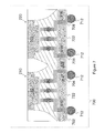
- FIG. 1 illustrates cross sectional views of a wafer after a dicing process in accordance with an embodiment
- FIG. 2 illustrates fabrication procedures for generating the step recesses in accordance with an embodiment
- FIG. 3 illustrates a process of stacking a plurality of semiconductor dies on a supporting wafer
- FIG. 4 illustrates a cross sectional view of a three dimensional (3D) integrated circuit (IC) having an underfill material layer formed between the semiconductor dies and the supporting wafer;
- 3D three dimensional
- FIG. 5 illustrates a cross sectional view of a 3D IC having a molding compound layer formed on top of the wafer stack
- FIG. 6 illustrates a process of backside grinding of a wafer stack in accordance with an embodiment
- FIG. 7 illustrates a cross sectional view of a 3D IC after a grinding process of a supporting wafer
- FIG. 8 illustrates cross sectional views of a wafer after a two-step dicing process in accordance with another embodiment
- FIG. 9 illustrates cross sectional views of a wafer after a two-step dicing process in accordance with yet another embodiment
- FIG. 10 illustrates cross sectional views of a wafer after a two-step dicing process in accordance with yet another embodiment
- FIG. 11 illustrates cross sectional views of a wafer after a two-step dicing process in accordance with yet another embodiment.
- FIG. 12 illustrates cross sectional views of a wafer after a two-step dicing process in accordance with yet another embodiment.
- IC three-dimensional integrated circuits
- FIG. 1 cross sectional views of a wafer after a dicing process are illustrated in accordance with an embodiment.
- the wafer 100 may comprise a plurality of integrated circuits.
- semiconductor dies e.g., semiconductor die 110
- a first cross sectional view is taken along the dashed line x-x′.
- the first cross section view includes a first semiconductor die 110 and a second semiconductor die 120 .
- a second cross sectional view is taken along the dashed line y-y′.
- the second cross section view includes the first semiconductor die 110 and a third semiconductor die 160 .
- the three semiconductor dies 110 , 120 and 160 shown in FIG. 1 have a substantially identical structure.
- the first semiconductor die 110 is described in detail below.
- the first semiconductor die 110 , the second semiconductor die 120 and the third semiconductor die 160 are drawn without details.
- the first semiconductor die 110 , the second semiconductor die 120 and the third semiconductor die 160 may comprise basic semiconductor layers such as active circuit layers, substrate layers, inter-layer dielectric (ILD) layers and inter-metal dielectric (IMD) layers (not shown).
- the first semiconductor die 110 comprises a substrate 102 .
- the substrate 102 may be a silicon substrate.
- the substrate 102 may be a silicon-on-insulator substrate.
- the substrate 102 may further comprise a variety of electrical circuits (not shown).
- the electrical circuits formed on the substrate 102 may be any type of circuitry suitable for a particular application.
- the electrical circuits may include various n-type metal-oxide semiconductor (NMOS) and/or p-type metal-oxide semiconductor (PMOS) devices such as transistors, capacitors, resistors, diodes, photo-diodes, fuses and the like.
- the electrical circuits may be interconnected to perform one or more functions.
- the functions may include memory structures, processing structures, sensors, amplifiers, power distribution, input/output circuitry or the like.
- the isolation layer 104 is formed on top of the substrate 102 .
- the isolation layer 104 may be formed, for example, of a low-K dielectric material, such as silicon oxide.
- the isolation layer 104 may be formed by any suitable method known in the art, such as spinning, chemical vapor deposition (CVD) and plasma enhanced chemical vapor deposition (PECVD). It should also be noted that one skilled in the art will recognize that the isolation layer 104 may further comprise a plurality of dielectric layers.
- a redistribution layer (RDL) 106 is formed on top of the isolation layer 104 .
- the active circuit layer (not shown) of the first semiconductor die 110 may be bridged by the RDL layer 106 so that the active circuit layer of the first semiconductor die 110 can be coupled to the input and output (I/O) terminals of the semiconductor die 110 .
- a plurality of under bump metal (UBM) structures 108 are formed on top of the RDL layer 106 .
- Interconnection bumps 112 , 114 and 116 are formed on top of the UBM structures 108 .
- the UBM structures 108 may help to prevent diffusion between the interconnection bumps (e.g., interconnection bump 112 ) and the integrated circuits of the first semiconductor die 110 , while providing a low resistance electrical connection.
- the interconnection bumps provide an effective way to connect the first semiconductor die 110 with external circuits (not shown).
- the interconnection bumps are I/O terminals of the first semiconductor die 110 .
- the interconnection bumps e.g., interconnection bump 112
- the interconnection bumps may be a plurality of solder balls.
- the interconnection bumps may be a plurality of land grid array (LGA) pads.
- FIG. 1 further illustrates there may be four step recesses at each semiconductor die's substrate.
- the first semiconductor die 110 may include four step recesses on all four sides of the body of the first semiconductor die 110 . More particularly, two step recesses of the first semiconductor die 110 are illustrated in the first cross sectional view taken along the dashed line x-x′. Likewise, the other two step recesses of the first semiconductor die 110 are illustrated in the second cross sectional view taken along the dashed line y-y′.
- the step recess has a vertical recess depth a 1 ranging from about 20 um to about 300 um.
- the step recess length b 1 is in a range from about 20 um to about 200 um. The detailed fabrication procedures for generating the step recesses will be described in detail with respect to FIG. 2 .
- FIG. 2 illustrates fabrication procedures for generating the step recesses in accordance with an embodiment.
- a wafer 202 is cut based upon the dicing pattern of the wafer 202 .
- a first dicing saw (not shown) cuts through the thickness of the isolation layer 104 and about 100 um into the substrate 102 .
- the blade of the first dicing saw (not shown) has a thickness ranging from about 40 um to about 400 um.
- a trench 201 is formed in the substrate 102 .
- a wafer 204 illustrates there may be a plurality of integrated circuits embedded in the wafer 204 , each of which is enclosed by trenches (e.g., trench 201 ).
- a second dicing saw with a thin blade (not shown) is employed to cut through the thickness of the substrate 102 .
- the semiconductor dies e.g., semiconductor die 210
- Such a two-step dicing process leads to a semiconductor die (e.g., semiconductor die 210 ) with four step recesses at four sides of the body of the semiconductor die.
- a semiconductor die e.g., semiconductor die 210
- four step recesses at four sides of the body of the semiconductor die.
- the dimensions used in the previous example are selected purely for demonstration purposes and are not intended to limit the various embodiments to any particular size dimensions.
- One of ordinary skill in the art would recognize many variations, alternatives, and modifications. For example, by controlling the dicing depth of the first dicing step or employing a dicing saw with a different blade width, the trench dimension as well as the size of the step recess can be adjusted accordingly.
- step recesses can be created by using other dicing tools such as laser dicing tools.
- laser dicing tools The operation principles of laser dicing tools are well known in the art, and hence are not discussed in detail herein.
- FIGS. 3-7 are cross sectional views of intermediate stages in the making of a 3D IC in accordance with an embodiment.
- FIG. 3 illustrates a process of stacking a plurality of semiconductor dies on a supporting wafer. After the two-step dicing process shown in FIG. 2 , the semiconductor dies 210 and 220 are flipped and further bonded on a supporting wafer 310 through a reflow process.
- the supporting wafer 310 may be alternatively referred to as a package substrate.
- the package substrate may be made of ceramic materials, organic materials and/or the like.
- the supporting wafer 310 may comprise a plurality of vias embedded in the substrate of the supporting wafer 310 .
- the active circuits of the semiconductor dies are coupled to the vias of the supporting wafer 310 through a conductive channel formed by the RDL layers on the supporting wafer (e.g., RDL layer 322 ), the interconnection bumps connected between the supporting wafer 310 and the semiconductor dies (e.g., semiconductor die 210 ).
- FIG. 4 illustrates a cross sectional view of a 3D IC having an underfill material layer formed between the semiconductor dies and the supporting wafer.
- An underfill material 402 may be formed in the gap between the supporting wafer 302 and the plurality of semiconductor dies (e.g., the first semiconductor die 102 ) mounted on top of the wafer 302 .
- the underfill material 402 may be an epoxy, which is dispensed at the gap between the supporting wafer 302 and the first semiconductor die 102 .
- the epoxy may be applied in a liquid form, and may harden after a curing process.
- the height of the underfill material layer 402 is controlled by the step recesses (e.g., step recess 404 ). In other words, such a step recess creates a ceiling for the underfill material layer 402 .
- a top non-recess portion of the first semiconductor die 210 , a recess of the first semiconductor die 210 , a top non-recess portion of the second semiconductor die 220 , a recess of the second semiconductor die 220 are embedded in the underfill material layer 402 .
- the underfill layer 402 may be formed of curable materials such as polymer based materials, resin based materials, polyimide, epoxy and any combinations of thereof.
- the underfill layer 402 can be formed by a spin-on coating process, dry film lamination process and/or the like.
- An advantageous feature of having an underfill material e.g., underfill material 402
- the underfill material 402 helps to prevent the wafer stack 400 from cracking.
- another advantage feature is that the underfill material 402 may help to reduce the mechanical and thermal stresses during the fabrication process of the wafer stack 400 .
- FIG. 5 illustrates a cross sectional view of a 3D IC having a molding compound layer formed on top of the wafer stack.
- the first semiconductor die 210 and the second semiconductor die 220 are embedded in a molding compound layer 502 .
- the molding compound layer 502 may be formed of curable materials such as polymer based materials, resin based materials, polyimide, epoxy and any combinations of thereof.
- the molding compound layer 502 can be formed by a spin-on coating process, an injection molding process and/or the like.
- the molding compound layer 502 is employed to keep the supporting wafer 302 and the semiconductor dies on top of the supporting wafer from cracking, bending, warping and/or the like.
- FIG. 6 illustrates a process of backside grinding of a wafer stack in accordance with an embodiment.
- the backside of the semiconductor dies 210 and 220 undergo a thinning process.
- the thinning process can employ a mechanical grinding process, a chemical polishing process, an etching process or the like.
- the backside of the semiconductor dies 210 and 220 can be ground so that the semiconductor dies 210 and 220 may have a thickness of approximately sub-100 um.
- the thickness of the semiconductor dies 210 and 220 may be reduced to a range from about 20 um to about 500 um.
- FIG. 7 illustrates a cross sectional view of a 3D IC after a grinding process of a supporting wafer. Similar to the backside grinding process of the semiconductor dies, a thinning process is employed to grind the supporting wafer 302 until the embedded ends of the vias (e.g., via 312 ) become exposed. Subsequently, an isolation layer 722 as well as redistribution layers 702 , 704 , 706 and 708 is formed on top of the newly ground backside of the supporting wafer 302 .
- a thinning process is employed to grind the supporting wafer 302 until the embedded ends of the vias (e.g., via 312 ) become exposed.
- an isolation layer 722 as well as redistribution layers 702 , 704 , 706 and 708 is formed on top of the newly ground backside of the supporting wafer 302 .
- a plurality of UBM structures may be formed on top of the redistribution layers 702 , 704 , 706 and 708 .
- the UBM structures may help to prevent diffusion between the solder balls and the integrated circuits of the multi-chip semiconductor device, while providing a low resistance electrical connection.
- a plurality of bumps 712 are formed on top of the UBM structures. Some bumps 712 may be formed on top of the exposed ends of the vias (e.g., via 312 ). It should be noted the bumps 712 may be formed somewhere other than the exposed ends of the vias and reconnected with the vias (e.g., via 314 ) through the redistribution layer 704 .
- FIG. 8 illustrates cross sectional views of a wafer after a two-step dicing process in accordance with another embodiment.
- the cross sectional views of a wafer 800 are similar to the cross sectional views of the wafer 100 shown in FIG. 1 except that during the second step of the dicing process, the trenches in the x-x′ direction are cut through by a thin blade 834 along one sidewall of the trenches rather than the middle line of trenches.
- a semiconductor die may include three step recesses rather than four step recesses shown in FIG. 1 .
- the semiconductor die 802 may include three step recesses.
- the side of the semiconductor die 802 not having a step recess is indicated by a dashed circle 812 .
- the dicing process of a wafer is well known in the art, and hence is not discussed in detail herein.
- FIG. 9 illustrates cross sectional views of a wafer after a two-step dicing process in accordance with yet another embodiment.
- the cross sectional views of a wafer 900 are similar to the cross sectional views of the wafer 100 shown in FIG. 1 except that during the second step of the dicing process, the trenches are cut through by a thin blade 934 along one sidewall of the trenches rather than the middle line of the trenches.
- a semiconductor die may include two step recesses.
- the semiconductor die 902 may include two step recesses. The sides of the semiconductor die 902 not having a step recess are indicated by dashed circles 912 and 916 .
- FIG. 10 illustrates cross sectional views of a wafer after a two-step dicing process in accordance with yet another embodiment.
- the cross sectional views of a wafer 1000 are similar to the cross sectional views of the wafer 100 shown in FIG. 1 except that during the first step of the dicing process, the thick blade 1032 is only applied to the trenches along the y-y′ direction.
- the trenches in the y-y′ direction are cut through by a thin blade 1034 along one sidewall of the trenches rather than the middle line of the trenches.
- a semiconductor die may include one step recesses.
- the semiconductor die 1002 may include one step recess. The sides of the semiconductor die 1002 not having a step recess are indicated by dashed circles 1012 , 1014 and 1016 .
- FIG. 11 illustrates cross sectional views of a wafer after a two-step dicing process in accordance with yet another embodiment.
- the cross sectional views of a wafer 1100 are similar to the cross sectional views of the wafer 100 shown in FIG. 1 except that there may be a slope (e.g., slope 1112 and slope 1114 ) rather than a step recess at each side of the body of the semiconductor 1102 .
- FIG. 12 illustrates cross sectional views of a wafer after a two-step dicing process in accordance with yet another embodiment.
- the cross sectional views of a wafer 1200 are similar to the cross sectional views of the wafer 100 shown in FIG.
- the semiconductor dies after a dicing process may include a step recess, a slope or a curved shape at each side of the body of the semiconductor dies. It is within the scope and spirit of various embodiments for the semiconductor dies to comprise other shapes.
Abstract
Description
Claims (14)
Priority Applications (3)
| Application Number | Priority Date | Filing Date | Title |
|---|---|---|---|
| US13/297,992 US8772929B2 (en) | 2011-11-16 | 2011-11-16 | Package for three dimensional integrated circuit |
| TW101112571A TWI490991B (en) | 2011-11-16 | 2012-04-10 | Package for three dimensional integrated circuit |
| US14/323,960 US9337063B2 (en) | 2011-11-16 | 2014-07-03 | Package for three dimensional integrated circuit |
Applications Claiming Priority (1)
| Application Number | Priority Date | Filing Date | Title |
|---|---|---|---|
| US13/297,992 US8772929B2 (en) | 2011-11-16 | 2011-11-16 | Package for three dimensional integrated circuit |
Related Child Applications (1)
| Application Number | Title | Priority Date | Filing Date |
|---|---|---|---|
| US14/323,960 Division US9337063B2 (en) | 2011-11-16 | 2014-07-03 | Package for three dimensional integrated circuit |
Publications (2)
| Publication Number | Publication Date |
|---|---|
| US20130119533A1 US20130119533A1 (en) | 2013-05-16 |
| US8772929B2 true US8772929B2 (en) | 2014-07-08 |
Family
ID=48279808
Family Applications (2)
| Application Number | Title | Priority Date | Filing Date |
|---|---|---|---|
| US13/297,992 Active US8772929B2 (en) | 2011-11-16 | 2011-11-16 | Package for three dimensional integrated circuit |
| US14/323,960 Active US9337063B2 (en) | 2011-11-16 | 2014-07-03 | Package for three dimensional integrated circuit |
Family Applications After (1)
| Application Number | Title | Priority Date | Filing Date |
|---|---|---|---|
| US14/323,960 Active US9337063B2 (en) | 2011-11-16 | 2014-07-03 | Package for three dimensional integrated circuit |
Country Status (2)
| Country | Link |
|---|---|
| US (2) | US8772929B2 (en) |
| TW (1) | TWI490991B (en) |
Cited By (2)
| Publication number | Priority date | Publication date | Assignee | Title |
|---|---|---|---|---|
| US10964681B2 (en) * | 2018-08-03 | 2021-03-30 | Toshiba Memory Corporation | Semiconductor device and method for manufacturing the same |
| US20230061968A1 (en) * | 2021-08-30 | 2023-03-02 | Taiwan Semiconductor Manufacturing Company, Ltd. | Semiconductor package and method of forming the same |
Families Citing this family (28)
| Publication number | Priority date | Publication date | Assignee | Title |
|---|---|---|---|---|
| US9385095B2 (en) | 2010-02-26 | 2016-07-05 | Taiwan Semiconductor Manufacturing Company, Ltd. | 3D semiconductor package interposer with die cavity |
| US9824924B2 (en) * | 2013-03-29 | 2017-11-21 | Stmicroelectronics Pte Ltd. | Semiconductor packages having an electric device with a recess |
| US9653443B2 (en) | 2014-02-14 | 2017-05-16 | Taiwan Semiconductor Manufacturing Company, Ltd. | Thermal performance structure for semiconductor packages and method of forming same |
| US10026671B2 (en) * | 2014-02-14 | 2018-07-17 | Taiwan Semiconductor Manufacturing Company, Ltd. | Substrate design for semiconductor packages and method of forming same |
| US10056267B2 (en) | 2014-02-14 | 2018-08-21 | Taiwan Semiconductor Manufacturing Company, Ltd. | Substrate design for semiconductor packages and method of forming same |
| US9768090B2 (en) | 2014-02-14 | 2017-09-19 | Taiwan Semiconductor Manufacturing Company, Ltd. | Substrate design for semiconductor packages and method of forming same |
| US9935090B2 (en) | 2014-02-14 | 2018-04-03 | Taiwan Semiconductor Manufacturing Company, Ltd. | Substrate design for semiconductor packages and method of forming same |
| KR101598688B1 (en) | 2014-03-25 | 2016-02-29 | 앰코 테크놀로지 코리아 주식회사 | Manufacturing method of semiconductor device and semiconductor device thereof |
| US9349670B2 (en) | 2014-08-04 | 2016-05-24 | Micron Technology, Inc. | Semiconductor die assemblies with heat sink and associated systems and methods |
| JP5967629B2 (en) | 2014-11-17 | 2016-08-10 | インターナショナル・ビジネス・マシーンズ・コーポレーションInternational Business Machines Corporation | Circuit module and manufacturing method thereof |
| US9564416B2 (en) | 2015-02-13 | 2017-02-07 | Taiwan Semiconductor Manufacturing Company, Ltd. | Package structures and methods of forming the same |
| JP6479532B2 (en) * | 2015-03-30 | 2019-03-06 | ルネサスエレクトロニクス株式会社 | Semiconductor device manufacturing method |
| US10075657B2 (en) | 2015-07-21 | 2018-09-11 | Fermi Research Alliance, Llc | Edgeless large area camera system |
| US10352991B2 (en) | 2015-07-21 | 2019-07-16 | Fermi Research Alliance, Llc | Edgeless large area ASIC |
| KR20170065397A (en) | 2015-12-03 | 2017-06-13 | 삼성전자주식회사 | Semiconductor device |
| US9589941B1 (en) * | 2016-01-15 | 2017-03-07 | Taiwan Semiconductor Manufacturing Company, Ltd. | Multi-chip package system and methods of forming the same |
| US10340213B2 (en) * | 2016-03-14 | 2019-07-02 | Amkor Technology, Inc. | Semiconductor device and manufacturing method thereof |
| US10720360B2 (en) * | 2016-07-29 | 2020-07-21 | Taiwan Semiconductor Manufacturing Company, Ltd. | Semiconductor die singulation and structures formed thereby |
| KR102442622B1 (en) | 2017-08-03 | 2022-09-13 | 삼성전자주식회사 | Semiconductor device package |
| CN108346639B (en) | 2017-09-30 | 2020-04-03 | 中芯集成电路(宁波)有限公司 | Wafer level system packaging method and packaging structure |
| CN107887350A (en) * | 2017-10-13 | 2018-04-06 | 中芯长电半导体(江阴)有限公司 | Semiconductor package and preparation method thereof |
| EP3706171A4 (en) | 2017-11-01 | 2021-04-21 | Sony Semiconductor Solutions Corporation | Imaging element, imaging device, electronic apparatus, and method for manufacturing imaging element |
| JP7048153B2 (en) * | 2018-04-25 | 2022-04-05 | ラピスセミコンダクタ株式会社 | Semiconductor devices and methods for manufacturing semiconductor devices |
| KR102518803B1 (en) | 2018-10-24 | 2023-04-07 | 삼성전자주식회사 | Semiconductor package |
| US11557559B2 (en) * | 2021-02-26 | 2023-01-17 | Taiwan Semiconductor Manufacturing Company, Ltd. | Package structure |
| US20230014470A1 (en) * | 2021-07-16 | 2023-01-19 | Nxp B.V | Packaged semiconductor devices and methods therefor |
| US11901256B2 (en) * | 2021-08-31 | 2024-02-13 | Taiwan Semiconductor Manufacturing Company, Ltd. | Semiconductor device, semiconductor package, and methods of manufacturing the same |
| TWI784847B (en) * | 2021-12-17 | 2022-11-21 | 力成科技股份有限公司 | Package structure and manufacturing method thereof |
Citations (58)
| Publication number | Priority date | Publication date | Assignee | Title |
|---|---|---|---|---|
| US4811082A (en) | 1986-11-12 | 1989-03-07 | International Business Machines Corporation | High performance integrated circuit packaging structure |
| US4990462A (en) | 1989-04-12 | 1991-02-05 | Advanced Micro Devices, Inc. | Method for coplanar integration of semiconductor ic devices |
| US5075253A (en) | 1989-04-12 | 1991-12-24 | Advanced Micro Devices, Inc. | Method of coplanar integration of semiconductor IC devices |
| US5380681A (en) | 1994-03-21 | 1995-01-10 | United Microelectronics Corporation | Three-dimensional multichip package and methods of fabricating |
| US6002177A (en) | 1995-12-27 | 1999-12-14 | International Business Machines Corporation | High density integrated circuit packaging with chip stacking and via interconnections |
| US6229216B1 (en) | 1999-01-11 | 2001-05-08 | Intel Corporation | Silicon interposer and multi-chip-module (MCM) with through substrate vias |
| US6271059B1 (en) | 1999-01-04 | 2001-08-07 | International Business Machines Corporation | Chip interconnection structure using stub terminals |
| US6279815B1 (en) | 1998-06-17 | 2001-08-28 | International Business Machines Corporation | Stacked chip process carrier |
| US6355501B1 (en) | 2000-09-21 | 2002-03-12 | International Business Machines Corporation | Three-dimensional chip stacking assembly |
| US6434016B2 (en) | 1999-06-18 | 2002-08-13 | Intel Corporation | Apparatus for interconnecting multiple devices on a circuit board |
| US6448661B1 (en) | 2001-02-09 | 2002-09-10 | Samsung Electornics Co., Ltd. | Three-dimensional multi-chip package having chip selection pads and manufacturing method thereof |
| US6461895B1 (en) | 1999-01-05 | 2002-10-08 | Intel Corporation | Process for making active interposer for high performance packaging applications |
| US6570248B1 (en) | 1998-08-31 | 2003-05-27 | Micron Technology, Inc. | Structure and method for a high-performance electronic packaging assembly |
| US6600222B1 (en) | 2002-07-17 | 2003-07-29 | Intel Corporation | Stacked microelectronic packages |
| US6607938B2 (en) | 2001-07-19 | 2003-08-19 | Samsung Electronics Co., Ltd. | Wafer level stack chip package and method for manufacturing same |
| US6661085B2 (en) | 2002-02-06 | 2003-12-09 | Intel Corporation | Barrier structure against corrosion and contamination in three-dimensional (3-D) wafer-to-wafer vertical stack |
| US6762076B2 (en) | 2002-02-20 | 2004-07-13 | Intel Corporation | Process of vertically stacking multiple wafers supporting different active integrated circuit (IC) devices |
| US6790748B2 (en) | 2002-12-19 | 2004-09-14 | Intel Corporation | Thinning techniques for wafer-to-wafer vertical stacks |
| US6887769B2 (en) | 2002-02-06 | 2005-05-03 | Intel Corporation | Dielectric recess for wafer-to-wafer and die-to-die metal bonding and method of fabricating the same |
| US6908565B2 (en) | 2002-12-24 | 2005-06-21 | Intel Corporation | Etch thinning techniques for wafer-to-wafer vertical stacks |
| US6908785B2 (en) | 2001-12-06 | 2005-06-21 | Samsung Electronics Co., Ltd. | Multi-chip package (MCP) with a conductive bar and method for manufacturing the same |
| US6924551B2 (en) | 2003-05-28 | 2005-08-02 | Intel Corporation | Through silicon via, folded flex microelectronic package |
| US6943067B2 (en) | 2002-01-08 | 2005-09-13 | Advanced Micro Devices, Inc. | Three-dimensional integrated semiconductor devices |
| US6946384B2 (en) | 2003-06-06 | 2005-09-20 | Intel Corporation | Stacked device underfill and a method of fabrication |
| US6975016B2 (en) | 2002-02-06 | 2005-12-13 | Intel Corporation | Wafer bonding using a flexible bladder press and thinned wafers for three-dimensional (3D) wafer-to-wafer vertical stack integration, and application thereof |
| US7087538B2 (en) | 2004-08-16 | 2006-08-08 | Intel Corporation | Method to fill the gap between coupled wafers |
| US7151009B2 (en) | 2004-06-18 | 2006-12-19 | Samsung Electronics Co., Ltd. | Method for manufacturing wafer level chip stack package |
| US7215033B2 (en) | 2003-11-19 | 2007-05-08 | Samsung Electronics Co., Ltd. | Wafer level stack structure for system-in-package and method thereof |
| US20070132089A1 (en) * | 2005-12-13 | 2007-06-14 | Tongbi Jiang | Microelectronic devices and methods for manufacturing microelectronic devices |
| US20070148918A1 (en) * | 2000-06-02 | 2007-06-28 | Kinsman Larry D | Method for fabricating a chip scale package using wafer level processing |
| US7276799B2 (en) | 2003-08-26 | 2007-10-02 | Samsung Electronics Co., Ltd. | Chip stack package and manufacturing method thereof |
| US7279795B2 (en) | 2005-12-29 | 2007-10-09 | Intel Corporation | Stacked die semiconductor package |
| US7307005B2 (en) | 2004-06-30 | 2007-12-11 | Intel Corporation | Wafer bonding with highly compliant plate having filler material enclosed hollow core |
| US7317256B2 (en) | 2005-06-01 | 2008-01-08 | Intel Corporation | Electronic packaging including die with through silicon via |
| US7320928B2 (en) | 2003-06-20 | 2008-01-22 | Intel Corporation | Method of forming a stacked device filler |
| US7345350B2 (en) | 2003-09-23 | 2008-03-18 | Micron Technology, Inc. | Process and integration scheme for fabricating conductive components, through-vias and semiconductor components including conductive through-wafer vias |
| US7402515B2 (en) | 2005-06-28 | 2008-07-22 | Intel Corporation | Method of forming through-silicon vias with stress buffer collars and resulting devices |
| US7402442B2 (en) | 2005-12-21 | 2008-07-22 | International Business Machines Corporation | Physically highly secure multi-chip assembly |
| US7410884B2 (en) | 2005-11-21 | 2008-08-12 | Intel Corporation | 3D integrated circuits using thick metal for backside connections and offset bumps |
| US7432592B2 (en) | 2005-10-13 | 2008-10-07 | Intel Corporation | Integrated micro-channels for 3D through silicon architectures |
| US7482702B2 (en) * | 2002-03-06 | 2009-01-27 | Micron Technology, Inc. | Semiconductor component sealed on five sides by polymer sealing layer |
| US7494845B2 (en) | 2004-06-22 | 2009-02-24 | Samsung Electronics Co., Ltd. | Method of forming a thin wafer stack for a wafer level package |
| US20090065902A1 (en) * | 2007-09-11 | 2009-03-12 | Cheemen Yu | Method of forming a semiconductor die having a sloped edge for receiving an electrical connector |
| US20090072332A1 (en) * | 2006-03-20 | 2009-03-19 | Koniklijke Phillips Electronics N.V | System-in-package platform for electronic-microfluidic devices |
| US20090079041A1 (en) * | 2007-09-24 | 2009-03-26 | Stats Chippac, Ltd. | Semiconductor Package and Method of Reducing Electromagnetic Interference Between Devices |
| US7528494B2 (en) | 2005-11-03 | 2009-05-05 | International Business Machines Corporation | Accessible chip stack and process of manufacturing thereof |
| US7557597B2 (en) | 2005-06-03 | 2009-07-07 | International Business Machines Corporation | Stacked chip security |
| US20090189279A1 (en) * | 2008-01-24 | 2009-07-30 | National Semiconductor Corporation | Methods and systems for packaging integrated circuits |
| US7576435B2 (en) | 2007-04-27 | 2009-08-18 | Taiwan Semiconductor Manufacturing Company, Ltd. | Low-cost and ultra-fine integrated circuit packaging technique |
| US7667335B2 (en) * | 2007-09-20 | 2010-02-23 | Stats Chippac, Ltd. | Semiconductor package with passivation island for reducing stress on solder bumps |
| US7834450B2 (en) | 2007-08-20 | 2010-11-16 | Samsung Electronics Co., Ltd. | Semiconductor package having memory devices stacked on logic device |
| US20120049358A1 (en) * | 2010-08-24 | 2012-03-01 | Bin-Hong Cheng | Semiconductor Device and Semiconductor Process for Making the Same |
| US20120146177A1 (en) * | 2010-12-09 | 2012-06-14 | Stats Chippac, Ltd. | Semiconductor Device and Method of Forming Recesses in Substrate for Same Size or Different Sized Die with Vertical Integration |
| US20120279287A1 (en) * | 2011-05-05 | 2012-11-08 | International Business Machines Corporation | Transferable Probe Tips |
| US20120286701A1 (en) * | 2011-05-09 | 2012-11-15 | Fang Sheng | Light Emitting Diode Light Source With Layered Phosphor Conversion Coating |
| US8338941B2 (en) * | 2009-07-21 | 2012-12-25 | Samsung Electronics Co., Ltd. | Semiconductor packages and methods of fabricating the same |
| US20130026609A1 (en) * | 2010-01-18 | 2013-01-31 | Marvell World Trade Ltd. | Package assembly including a semiconductor substrate with stress relief structure |
| US8399987B2 (en) * | 2009-12-04 | 2013-03-19 | Samsung Electronics Co., Ltd. | Microelectronic devices including conductive vias, conductive caps and variable thickness insulating layers |
Family Cites Families (10)
| Publication number | Priority date | Publication date | Assignee | Title |
|---|---|---|---|---|
| JP3497722B2 (en) * | 1998-02-27 | 2004-02-16 | 富士通株式会社 | Semiconductor device, method of manufacturing the same, and transfer tray thereof |
| US6281047B1 (en) * | 2000-11-10 | 2001-08-28 | Siliconware Precision Industries, Co., Ltd. | Method of singulating a batch of integrated circuit package units constructed on a single matrix base |
| US6727576B2 (en) * | 2001-10-31 | 2004-04-27 | Infineon Technologies Ag | Transfer wafer level packaging |
| TW557485B (en) | 2001-11-26 | 2003-10-11 | Shindo Denshi Kogyo Kk | Semiconductor device and method of IC-mounting for semiconductor device |
| TWI236747B (en) * | 2004-03-12 | 2005-07-21 | Advanced Semiconductor Eng | Manufacturing process and structure for a flip-chip package |
| US20060019468A1 (en) * | 2004-07-21 | 2006-01-26 | Beatty John J | Method of manufacturing a plurality of electronic assemblies |
| US9875911B2 (en) * | 2009-09-23 | 2018-01-23 | STATS ChipPAC Pte. Ltd. | Semiconductor device and method of forming interposer with opening to contain semiconductor die |
| TWI505433B (en) * | 2009-10-01 | 2015-10-21 | Xintec Inc | Chip package and fabrication method thereof |
| KR101715761B1 (en) * | 2010-12-31 | 2017-03-14 | 삼성전자주식회사 | Semiconductor packages and methods for fabricating the same |
| TWI557485B (en) * | 2014-11-20 | 2016-11-11 | 群創光電股份有限公司 | Display panel |
-
2011
- 2011-11-16 US US13/297,992 patent/US8772929B2/en active Active
-
2012
- 2012-04-10 TW TW101112571A patent/TWI490991B/en active
-
2014
- 2014-07-03 US US14/323,960 patent/US9337063B2/en active Active
Patent Citations (68)
| Publication number | Priority date | Publication date | Assignee | Title |
|---|---|---|---|---|
| US4811082A (en) | 1986-11-12 | 1989-03-07 | International Business Machines Corporation | High performance integrated circuit packaging structure |
| US4990462A (en) | 1989-04-12 | 1991-02-05 | Advanced Micro Devices, Inc. | Method for coplanar integration of semiconductor ic devices |
| US5075253A (en) | 1989-04-12 | 1991-12-24 | Advanced Micro Devices, Inc. | Method of coplanar integration of semiconductor IC devices |
| US5380681A (en) | 1994-03-21 | 1995-01-10 | United Microelectronics Corporation | Three-dimensional multichip package and methods of fabricating |
| US5481133A (en) | 1994-03-21 | 1996-01-02 | United Microelectronics Corporation | Three-dimensional multichip package |
| US6236115B1 (en) | 1995-12-27 | 2001-05-22 | International Business Machines Corporation | High density integrated circuit packaging with chip stacking and via interconnections |
| US6002177A (en) | 1995-12-27 | 1999-12-14 | International Business Machines Corporation | High density integrated circuit packaging with chip stacking and via interconnections |
| US6187678B1 (en) | 1995-12-27 | 2001-02-13 | International Business Machines Corporation | High density integrated circuit packaging with chip stacking and via interconnections |
| US6279815B1 (en) | 1998-06-17 | 2001-08-28 | International Business Machines Corporation | Stacked chip process carrier |
| US6570248B1 (en) | 1998-08-31 | 2003-05-27 | Micron Technology, Inc. | Structure and method for a high-performance electronic packaging assembly |
| US6271059B1 (en) | 1999-01-04 | 2001-08-07 | International Business Machines Corporation | Chip interconnection structure using stub terminals |
| US6461895B1 (en) | 1999-01-05 | 2002-10-08 | Intel Corporation | Process for making active interposer for high performance packaging applications |
| US6562653B1 (en) | 1999-01-11 | 2003-05-13 | Intel Corporation | Silicon interposer and multi-chip-module (MCM) with through substrate vias |
| US6229216B1 (en) | 1999-01-11 | 2001-05-08 | Intel Corporation | Silicon interposer and multi-chip-module (MCM) with through substrate vias |
| US6434016B2 (en) | 1999-06-18 | 2002-08-13 | Intel Corporation | Apparatus for interconnecting multiple devices on a circuit board |
| US7727858B2 (en) * | 2000-06-02 | 2010-06-01 | Micron Technology, Inc. | Method for fabricating a chip scale package using wafer level processing |
| US20070148918A1 (en) * | 2000-06-02 | 2007-06-28 | Kinsman Larry D | Method for fabricating a chip scale package using wafer level processing |
| US6355501B1 (en) | 2000-09-21 | 2002-03-12 | International Business Machines Corporation | Three-dimensional chip stacking assembly |
| US6448661B1 (en) | 2001-02-09 | 2002-09-10 | Samsung Electornics Co., Ltd. | Three-dimensional multi-chip package having chip selection pads and manufacturing method thereof |
| US6607938B2 (en) | 2001-07-19 | 2003-08-19 | Samsung Electronics Co., Ltd. | Wafer level stack chip package and method for manufacturing same |
| US7531890B2 (en) | 2001-12-06 | 2009-05-12 | Samsung Electronics Co., Ltd. | Multi-chip package (MCP) with a conductive bar and method for manufacturing the same |
| US6908785B2 (en) | 2001-12-06 | 2005-06-21 | Samsung Electronics Co., Ltd. | Multi-chip package (MCP) with a conductive bar and method for manufacturing the same |
| US6943067B2 (en) | 2002-01-08 | 2005-09-13 | Advanced Micro Devices, Inc. | Three-dimensional integrated semiconductor devices |
| US7037804B2 (en) | 2002-02-06 | 2006-05-02 | Intel Corporation | Wafer bonding using a flexible bladder press for three dimensional (3D) vertical stack integration |
| US6975016B2 (en) | 2002-02-06 | 2005-12-13 | Intel Corporation | Wafer bonding using a flexible bladder press and thinned wafers for three-dimensional (3D) wafer-to-wafer vertical stack integration, and application thereof |
| US6887769B2 (en) | 2002-02-06 | 2005-05-03 | Intel Corporation | Dielectric recess for wafer-to-wafer and die-to-die metal bonding and method of fabricating the same |
| US6661085B2 (en) | 2002-02-06 | 2003-12-09 | Intel Corporation | Barrier structure against corrosion and contamination in three-dimensional (3-D) wafer-to-wafer vertical stack |
| US7056807B2 (en) | 2002-02-06 | 2006-06-06 | Intel Corporation | Barrier structure against corrosion and contamination in three-dimensional (3-D) wafer-to-wafer vertical stack |
| US6762076B2 (en) | 2002-02-20 | 2004-07-13 | Intel Corporation | Process of vertically stacking multiple wafers supporting different active integrated circuit (IC) devices |
| US7157787B2 (en) | 2002-02-20 | 2007-01-02 | Intel Corporation | Process of vertically stacking multiple wafers supporting different active integrated circuit (IC) devices |
| US7482702B2 (en) * | 2002-03-06 | 2009-01-27 | Micron Technology, Inc. | Semiconductor component sealed on five sides by polymer sealing layer |
| US6600222B1 (en) | 2002-07-17 | 2003-07-29 | Intel Corporation | Stacked microelectronic packages |
| US6790748B2 (en) | 2002-12-19 | 2004-09-14 | Intel Corporation | Thinning techniques for wafer-to-wafer vertical stacks |
| US6908565B2 (en) | 2002-12-24 | 2005-06-21 | Intel Corporation | Etch thinning techniques for wafer-to-wafer vertical stacks |
| US6924551B2 (en) | 2003-05-28 | 2005-08-02 | Intel Corporation | Through silicon via, folded flex microelectronic package |
| US6946384B2 (en) | 2003-06-06 | 2005-09-20 | Intel Corporation | Stacked device underfill and a method of fabrication |
| US7320928B2 (en) | 2003-06-20 | 2008-01-22 | Intel Corporation | Method of forming a stacked device filler |
| US7276799B2 (en) | 2003-08-26 | 2007-10-02 | Samsung Electronics Co., Ltd. | Chip stack package and manufacturing method thereof |
| US7345350B2 (en) | 2003-09-23 | 2008-03-18 | Micron Technology, Inc. | Process and integration scheme for fabricating conductive components, through-vias and semiconductor components including conductive through-wafer vias |
| US7215033B2 (en) | 2003-11-19 | 2007-05-08 | Samsung Electronics Co., Ltd. | Wafer level stack structure for system-in-package and method thereof |
| US7151009B2 (en) | 2004-06-18 | 2006-12-19 | Samsung Electronics Co., Ltd. | Method for manufacturing wafer level chip stack package |
| US7494845B2 (en) | 2004-06-22 | 2009-02-24 | Samsung Electronics Co., Ltd. | Method of forming a thin wafer stack for a wafer level package |
| US7307005B2 (en) | 2004-06-30 | 2007-12-11 | Intel Corporation | Wafer bonding with highly compliant plate having filler material enclosed hollow core |
| US7087538B2 (en) | 2004-08-16 | 2006-08-08 | Intel Corporation | Method to fill the gap between coupled wafers |
| US7317256B2 (en) | 2005-06-01 | 2008-01-08 | Intel Corporation | Electronic packaging including die with through silicon via |
| US7557597B2 (en) | 2005-06-03 | 2009-07-07 | International Business Machines Corporation | Stacked chip security |
| US7402515B2 (en) | 2005-06-28 | 2008-07-22 | Intel Corporation | Method of forming through-silicon vias with stress buffer collars and resulting devices |
| US7432592B2 (en) | 2005-10-13 | 2008-10-07 | Intel Corporation | Integrated micro-channels for 3D through silicon architectures |
| US7528494B2 (en) | 2005-11-03 | 2009-05-05 | International Business Machines Corporation | Accessible chip stack and process of manufacturing thereof |
| US7410884B2 (en) | 2005-11-21 | 2008-08-12 | Intel Corporation | 3D integrated circuits using thick metal for backside connections and offset bumps |
| US20070132089A1 (en) * | 2005-12-13 | 2007-06-14 | Tongbi Jiang | Microelectronic devices and methods for manufacturing microelectronic devices |
| US7402442B2 (en) | 2005-12-21 | 2008-07-22 | International Business Machines Corporation | Physically highly secure multi-chip assembly |
| US7279795B2 (en) | 2005-12-29 | 2007-10-09 | Intel Corporation | Stacked die semiconductor package |
| US20130149215A1 (en) * | 2006-03-20 | 2013-06-13 | Koninklijke Philips Electronics N.V. | System-in-package platform for electronic-microfluidic devices |
| US20090072332A1 (en) * | 2006-03-20 | 2009-03-19 | Koniklijke Phillips Electronics N.V | System-in-package platform for electronic-microfluidic devices |
| US7576435B2 (en) | 2007-04-27 | 2009-08-18 | Taiwan Semiconductor Manufacturing Company, Ltd. | Low-cost and ultra-fine integrated circuit packaging technique |
| US7834450B2 (en) | 2007-08-20 | 2010-11-16 | Samsung Electronics Co., Ltd. | Semiconductor package having memory devices stacked on logic device |
| US20090065902A1 (en) * | 2007-09-11 | 2009-03-12 | Cheemen Yu | Method of forming a semiconductor die having a sloped edge for receiving an electrical connector |
| US7667335B2 (en) * | 2007-09-20 | 2010-02-23 | Stats Chippac, Ltd. | Semiconductor package with passivation island for reducing stress on solder bumps |
| US20090079041A1 (en) * | 2007-09-24 | 2009-03-26 | Stats Chippac, Ltd. | Semiconductor Package and Method of Reducing Electromagnetic Interference Between Devices |
| US20090189279A1 (en) * | 2008-01-24 | 2009-07-30 | National Semiconductor Corporation | Methods and systems for packaging integrated circuits |
| US8338941B2 (en) * | 2009-07-21 | 2012-12-25 | Samsung Electronics Co., Ltd. | Semiconductor packages and methods of fabricating the same |
| US8399987B2 (en) * | 2009-12-04 | 2013-03-19 | Samsung Electronics Co., Ltd. | Microelectronic devices including conductive vias, conductive caps and variable thickness insulating layers |
| US20130026609A1 (en) * | 2010-01-18 | 2013-01-31 | Marvell World Trade Ltd. | Package assembly including a semiconductor substrate with stress relief structure |
| US20120049358A1 (en) * | 2010-08-24 | 2012-03-01 | Bin-Hong Cheng | Semiconductor Device and Semiconductor Process for Making the Same |
| US20120146177A1 (en) * | 2010-12-09 | 2012-06-14 | Stats Chippac, Ltd. | Semiconductor Device and Method of Forming Recesses in Substrate for Same Size or Different Sized Die with Vertical Integration |
| US20120279287A1 (en) * | 2011-05-05 | 2012-11-08 | International Business Machines Corporation | Transferable Probe Tips |
| US20120286701A1 (en) * | 2011-05-09 | 2012-11-15 | Fang Sheng | Light Emitting Diode Light Source With Layered Phosphor Conversion Coating |
Cited By (3)
| Publication number | Priority date | Publication date | Assignee | Title |
|---|---|---|---|---|
| US10964681B2 (en) * | 2018-08-03 | 2021-03-30 | Toshiba Memory Corporation | Semiconductor device and method for manufacturing the same |
| US20230061968A1 (en) * | 2021-08-30 | 2023-03-02 | Taiwan Semiconductor Manufacturing Company, Ltd. | Semiconductor package and method of forming the same |
| US11854929B2 (en) * | 2021-08-30 | 2023-12-26 | Taiwan Semiconductor Manufacturing Company, Ltd. | Semiconductor package and method of forming the same |
Also Published As
| Publication number | Publication date |
|---|---|
| TW201322391A (en) | 2013-06-01 |
| TWI490991B (en) | 2015-07-01 |
| US20130119533A1 (en) | 2013-05-16 |
| US9337063B2 (en) | 2016-05-10 |
| US20140322866A1 (en) | 2014-10-30 |
Similar Documents
| Publication | Publication Date | Title |
|---|---|---|
| US8772929B2 (en) | Package for three dimensional integrated circuit | |
| US11488882B2 (en) | Die-on-interposer assembly with dam structure and method of manufacturing the same | |
| US20240105632A1 (en) | Method for Forming a Semiconductor Device Having TSV Formed Through a Silicon Interposer and a Second Silicon Substrate with Cavity Covering a Second Die | |
| US10971371B2 (en) | Multi-chip structure and method of forming same | |
| CN110504247B (en) | Integrated circuit package and method of forming the same | |
| US20210057383A1 (en) | Sawing Underfill in Packaging Processes | |
| US8518753B2 (en) | Assembly method for three dimensional integrated circuit | |
| US9679882B2 (en) | Method of multi-chip wafer level packaging | |
| US9412661B2 (en) | Method for forming package-on-package structure | |
| TWI556349B (en) | Semiconductor device structure and fabricating method thereof | |
| US9378982B2 (en) | Die package with openings surrounding end-portions of through package vias (TPVs) and package on package (PoP) using the die package | |
| US9911687B2 (en) | Molding compound structure | |
| US20130307149A1 (en) | Three-Dimensional Integrated Circuit (3DIC) | |
| US11380653B2 (en) | Die stack structure and manufacturing method thereof | |
| KR20130118757A (en) | Method of fabricating three dimensional integrated circuit | |
| US20130075892A1 (en) | Method for Three Dimensional Integrated Circuit Fabrication | |
| US9418876B2 (en) | Method of three dimensional integrated circuit assembly | |
| TW202213689A (en) | Die stack structure | |
| US20220352119A1 (en) | Multi-chip package having stress relief structure | |
| US20230402339A1 (en) | Molding Structures for Integrated Circuit Packages and Methods of Forming the Same |
Legal Events
| Date | Code | Title | Description |
|---|---|---|---|
| AS | Assignment |
Owner name: TAIWAN SEMICONDUCTOR MANUFACTURING COMPANY, LTD., Free format text: ASSIGNMENT OF ASSIGNORS INTEREST;ASSIGNORS:CHEN, CHIH-HAO;LEE, LONG HUA;SU, CHUN-HSING;AND OTHERS;SIGNING DATES FROM 20111111 TO 20111122;REEL/FRAME:027655/0540 |
|
| STCF | Information on status: patent grant |
Free format text: PATENTED CASE |
|
| MAFP | Maintenance fee payment |
Free format text: PAYMENT OF MAINTENANCE FEE, 4TH YEAR, LARGE ENTITY (ORIGINAL EVENT CODE: M1551) Year of fee payment: 4 |
|
| MAFP | Maintenance fee payment |
Free format text: PAYMENT OF MAINTENANCE FEE, 8TH YEAR, LARGE ENTITY (ORIGINAL EVENT CODE: M1552); ENTITY STATUS OF PATENT OWNER: LARGE ENTITY Year of fee payment: 8 |