US8901268B2 - Compositions, layers and films for optoelectronic devices, methods of production and uses thereof - Google Patents
Compositions, layers and films for optoelectronic devices, methods of production and uses thereof Download PDFInfo
- Publication number
- US8901268B2 US8901268B2 US12/027,113 US2711308A US8901268B2 US 8901268 B2 US8901268 B2 US 8901268B2 US 2711308 A US2711308 A US 2711308A US 8901268 B2 US8901268 B2 US 8901268B2
- Authority
- US
- United States
- Prior art keywords
- aryl
- film
- contemplated
- carbon
- percent
- Prior art date
- Legal status (The legal status is an assumption and is not a legal conclusion. Google has not performed a legal analysis and makes no representation as to the accuracy of the status listed.)
- Active, expires
Links
- 239000000203 mixture Substances 0.000 title claims abstract description 165
- 230000005693 optoelectronics Effects 0.000 title claims description 32
- 238000000034 method Methods 0.000 title description 40
- 238000004519 manufacturing process Methods 0.000 title description 12
- 239000002904 solvent Substances 0.000 claims abstract description 64
- 125000003118 aryl group Chemical group 0.000 claims abstract description 51
- 239000003054 catalyst Substances 0.000 claims abstract description 40
- 125000000217 alkyl group Chemical group 0.000 claims abstract description 35
- 239000002210 silicon-based material Substances 0.000 claims abstract description 28
- 239000010408 film Substances 0.000 claims description 183
- -1 phosphonium compound Chemical class 0.000 claims description 49
- 229910052799 carbon Inorganic materials 0.000 claims description 36
- OKTJSMMVPCPJKN-UHFFFAOYSA-N Carbon Chemical compound [C] OKTJSMMVPCPJKN-UHFFFAOYSA-N 0.000 claims description 35
- 239000004094 surface-active agent Substances 0.000 claims description 32
- 239000010409 thin film Substances 0.000 claims description 19
- 239000002318 adhesion promoter Substances 0.000 claims description 17
- 125000001997 phenyl group Chemical group [H]C1=C([H])C([H])=C(*)C([H])=C1[H] 0.000 claims description 17
- 238000002834 transmittance Methods 0.000 claims description 15
- 229910021417 amorphous silicon Inorganic materials 0.000 claims description 13
- 239000011159 matrix material Substances 0.000 claims description 11
- 239000004033 plastic Substances 0.000 claims description 11
- 229920003023 plastic Polymers 0.000 claims description 11
- 239000004973 liquid crystal related substance Substances 0.000 claims description 10
- 229910001220 stainless steel Inorganic materials 0.000 claims description 10
- 239000010935 stainless steel Substances 0.000 claims description 10
- 239000003431 cross linking reagent Substances 0.000 claims description 9
- 230000003287 optical effect Effects 0.000 claims description 9
- 150000001412 amines Chemical class 0.000 claims description 8
- 125000002496 methyl group Chemical group [H]C([H])([H])* 0.000 claims description 8
- 239000000654 additive Substances 0.000 claims description 7
- 238000009833 condensation Methods 0.000 claims description 6
- 230000005494 condensation Effects 0.000 claims description 6
- 229910021420 polycrystalline silicon Inorganic materials 0.000 claims description 5
- 230000000996 additive effect Effects 0.000 claims description 4
- 229920001921 poly-methyl-phenyl-siloxane Polymers 0.000 claims description 4
- 229920005591 polysilicon Polymers 0.000 claims description 4
- XYFCBTPGUUZFHI-UHFFFAOYSA-N Phosphine Natural products P XYFCBTPGUUZFHI-UHFFFAOYSA-N 0.000 claims description 3
- 150000003868 ammonium compounds Chemical class 0.000 claims description 3
- 229910021419 crystalline silicon Inorganic materials 0.000 claims description 3
- 230000005669 field effect Effects 0.000 claims description 3
- 230000006698 induction Effects 0.000 claims description 3
- 229910000073 phosphorus hydride Inorganic materials 0.000 claims description 3
- 230000003068 static effect Effects 0.000 claims description 3
- 239000000463 material Substances 0.000 description 161
- 239000010410 layer Substances 0.000 description 142
- 239000000758 substrate Substances 0.000 description 70
- 238000000576 coating method Methods 0.000 description 38
- 238000009472 formulation Methods 0.000 description 36
- 150000001875 compounds Chemical class 0.000 description 28
- 229910052751 metal Inorganic materials 0.000 description 27
- 239000002184 metal Substances 0.000 description 26
- 238000002161 passivation Methods 0.000 description 26
- 239000011521 glass Substances 0.000 description 24
- 229920000642 polymer Polymers 0.000 description 24
- 238000010943 off-gassing Methods 0.000 description 23
- KUCWUAFNGCMZDB-UHFFFAOYSA-N 2-amino-3-nitrophenol Chemical compound NC1=C(O)C=CC=C1[N+]([O-])=O KUCWUAFNGCMZDB-UHFFFAOYSA-N 0.000 description 22
- LLHKCFNBLRBOGN-UHFFFAOYSA-N propylene glycol methyl ether acetate Chemical compound COCC(C)OC(C)=O LLHKCFNBLRBOGN-UHFFFAOYSA-N 0.000 description 22
- 239000007787 solid Substances 0.000 description 21
- 235000012431 wafers Nutrition 0.000 description 21
- 239000003989 dielectric material Substances 0.000 description 20
- 229920002120 photoresistant polymer Polymers 0.000 description 20
- 239000011248 coating agent Substances 0.000 description 18
- 239000000470 constituent Substances 0.000 description 18
- WGTYBPLFGIVFAS-UHFFFAOYSA-M tetramethylammonium hydroxide Chemical compound [OH-].C[N+](C)(C)C WGTYBPLFGIVFAS-UHFFFAOYSA-M 0.000 description 18
- VYPSYNLAJGMNEJ-UHFFFAOYSA-N Silicium dioxide Chemical compound O=[Si]=O VYPSYNLAJGMNEJ-UHFFFAOYSA-N 0.000 description 17
- 230000008569 process Effects 0.000 description 17
- 230000004580 weight loss Effects 0.000 description 17
- 239000000126 substance Substances 0.000 description 16
- 238000002411 thermogravimetry Methods 0.000 description 16
- 238000012876 topography Methods 0.000 description 16
- 239000004065 semiconductor Substances 0.000 description 14
- NOKUWSXLHXMAOM-UHFFFAOYSA-N hydroxy(phenyl)silicon Chemical class O[Si]C1=CC=CC=C1 NOKUWSXLHXMAOM-UHFFFAOYSA-N 0.000 description 13
- KBXJHRABGYYAFC-UHFFFAOYSA-N octaphenylsilsesquioxane Chemical compound O1[Si](O2)(C=3C=CC=CC=3)O[Si](O3)(C=4C=CC=CC=4)O[Si](O4)(C=5C=CC=CC=5)O[Si]1(C=1C=CC=CC=1)O[Si](O1)(C=5C=CC=CC=5)O[Si]2(C=2C=CC=CC=2)O[Si]3(C=2C=CC=CC=2)O[Si]41C1=CC=CC=C1 KBXJHRABGYYAFC-UHFFFAOYSA-N 0.000 description 13
- XLYOFNOQVPJJNP-UHFFFAOYSA-N water Substances O XLYOFNOQVPJJNP-UHFFFAOYSA-N 0.000 description 13
- XUIMIQQOPSSXEZ-UHFFFAOYSA-N Silicon Chemical compound [Si] XUIMIQQOPSSXEZ-UHFFFAOYSA-N 0.000 description 12
- 238000011068 loading method Methods 0.000 description 12
- 229910052710 silicon Inorganic materials 0.000 description 12
- 239000010703 silicon Substances 0.000 description 12
- 238000005229 chemical vapour deposition Methods 0.000 description 11
- KPUWHANPEXNPJT-UHFFFAOYSA-N disiloxane Chemical class [SiH3]O[SiH3] KPUWHANPEXNPJT-UHFFFAOYSA-N 0.000 description 11
- WYTZZXDRDKSJID-UHFFFAOYSA-N (3-aminopropyl)triethoxysilane Chemical compound CCO[Si](OCC)(OCC)CCCN WYTZZXDRDKSJID-UHFFFAOYSA-N 0.000 description 10
- 230000004888 barrier function Effects 0.000 description 10
- 229910001868 water Inorganic materials 0.000 description 10
- 238000009792 diffusion process Methods 0.000 description 9
- 230000006870 function Effects 0.000 description 9
- 229930195733 hydrocarbon Natural products 0.000 description 8
- 150000002430 hydrocarbons Chemical class 0.000 description 8
- 239000011229 interlayer Substances 0.000 description 8
- 239000011347 resin Substances 0.000 description 8
- 229920005989 resin Polymers 0.000 description 8
- 238000004528 spin coating Methods 0.000 description 8
- 239000004215 Carbon black (E152) Substances 0.000 description 7
- 229910004205 SiNX Inorganic materials 0.000 description 7
- 229910052681 coesite Inorganic materials 0.000 description 7
- 229910052906 cristobalite Inorganic materials 0.000 description 7
- 238000004132 cross linking Methods 0.000 description 7
- 238000000151 deposition Methods 0.000 description 7
- 239000000377 silicon dioxide Substances 0.000 description 7
- 229910052682 stishovite Inorganic materials 0.000 description 7
- 229910052905 tridymite Inorganic materials 0.000 description 7
- 229920001621 AMOLED Polymers 0.000 description 6
- UHOVQNZJYSORNB-UHFFFAOYSA-N Benzene Chemical compound C1=CC=CC=C1 UHOVQNZJYSORNB-UHFFFAOYSA-N 0.000 description 6
- MUBZPKHOEPUJKR-UHFFFAOYSA-N Oxalic acid Chemical compound OC(=O)C(O)=O MUBZPKHOEPUJKR-UHFFFAOYSA-N 0.000 description 6
- YXFVVABEGXRONW-UHFFFAOYSA-N Toluene Chemical compound CC1=CC=CC=C1 YXFVVABEGXRONW-UHFFFAOYSA-N 0.000 description 6
- 230000015556 catabolic process Effects 0.000 description 6
- 230000003993 interaction Effects 0.000 description 6
- 238000005259 measurement Methods 0.000 description 6
- VLKZOEOYAKHREP-UHFFFAOYSA-N n-Hexane Chemical compound CCCCCC VLKZOEOYAKHREP-UHFFFAOYSA-N 0.000 description 6
- SECXISVLQFMRJM-UHFFFAOYSA-N NMP Substances CN1CCCC1=O SECXISVLQFMRJM-UHFFFAOYSA-N 0.000 description 5
- 230000008859 change Effects 0.000 description 5
- 238000006243 chemical reaction Methods 0.000 description 5
- KWIUHFFTVRNATP-UHFFFAOYSA-N glycine betaine Chemical compound C[N+](C)(C)CC([O-])=O KWIUHFFTVRNATP-UHFFFAOYSA-N 0.000 description 5
- 238000004377 microelectronic Methods 0.000 description 5
- 238000000059 patterning Methods 0.000 description 5
- 238000000623 plasma-assisted chemical vapour deposition Methods 0.000 description 5
- 239000004417 polycarbonate Substances 0.000 description 5
- 229920000515 polycarbonate Polymers 0.000 description 5
- 238000007764 slot die coating Methods 0.000 description 5
- IMNFDUFMRHMDMM-UHFFFAOYSA-N N-Heptane Chemical compound CCCCCCC IMNFDUFMRHMDMM-UHFFFAOYSA-N 0.000 description 4
- CTQNGGLPUBDAKN-UHFFFAOYSA-N O-Xylene Chemical compound CC1=CC=CC=C1C CTQNGGLPUBDAKN-UHFFFAOYSA-N 0.000 description 4
- OFBQJSOFQDEBGM-UHFFFAOYSA-N Pentane Chemical compound CCCCC OFBQJSOFQDEBGM-UHFFFAOYSA-N 0.000 description 4
- 229910020381 SiO1.5 Inorganic materials 0.000 description 4
- 238000010521 absorption reaction Methods 0.000 description 4
- 239000002253 acid Substances 0.000 description 4
- 239000000853 adhesive Substances 0.000 description 4
- 230000001070 adhesive effect Effects 0.000 description 4
- 229910052782 aluminium Inorganic materials 0.000 description 4
- 239000003990 capacitor Substances 0.000 description 4
- 229910052804 chromium Inorganic materials 0.000 description 4
- 239000011651 chromium Substances 0.000 description 4
- 230000007547 defect Effects 0.000 description 4
- 238000005516 engineering process Methods 0.000 description 4
- 230000002209 hydrophobic effect Effects 0.000 description 4
- 239000012535 impurity Substances 0.000 description 4
- 239000007788 liquid Substances 0.000 description 4
- 239000012044 organic layer Substances 0.000 description 4
- 239000000523 sample Substances 0.000 description 4
- 125000001424 substituent group Chemical group 0.000 description 4
- 230000003746 surface roughness Effects 0.000 description 4
- 238000012360 testing method Methods 0.000 description 4
- ZWEHNKRNPOVVGH-UHFFFAOYSA-N 2-Butanone Chemical compound CCC(C)=O ZWEHNKRNPOVVGH-UHFFFAOYSA-N 0.000 description 3
- JKXYOQDLERSFPT-UHFFFAOYSA-N 2-[2-[2-[2-[2-[2-[2-[2-[2-[2-[2-[2-[2-[2-[2-[2-[2-[2-[2-(2-octadecoxyethoxy)ethoxy]ethoxy]ethoxy]ethoxy]ethoxy]ethoxy]ethoxy]ethoxy]ethoxy]ethoxy]ethoxy]ethoxy]ethoxy]ethoxy]ethoxy]ethoxy]ethoxy]ethoxy]ethanol Chemical compound CCCCCCCCCCCCCCCCCCOCCOCCOCCOCCOCCOCCOCCOCCOCCOCCOCCOCCOCCOCCOCCOCCOCCOCCOCCOCCO JKXYOQDLERSFPT-UHFFFAOYSA-N 0.000 description 3
- CSCPPACGZOOCGX-UHFFFAOYSA-N Acetone Chemical compound CC(C)=O CSCPPACGZOOCGX-UHFFFAOYSA-N 0.000 description 3
- 230000004913 activation Effects 0.000 description 3
- 150000001298 alcohols Chemical class 0.000 description 3
- 150000001338 aliphatic hydrocarbons Chemical class 0.000 description 3
- QVGXLLKOCUKJST-UHFFFAOYSA-N atomic oxygen Chemical compound [O] QVGXLLKOCUKJST-UHFFFAOYSA-N 0.000 description 3
- UMIVXZPTRXBADB-UHFFFAOYSA-N benzocyclobutene Chemical compound C1=CC=C2CCC2=C1 UMIVXZPTRXBADB-UHFFFAOYSA-N 0.000 description 3
- 238000006482 condensation reaction Methods 0.000 description 3
- 239000008367 deionised water Substances 0.000 description 3
- 229910021641 deionized water Inorganic materials 0.000 description 3
- 230000008021 deposition Effects 0.000 description 3
- 150000002170 ethers Chemical class 0.000 description 3
- 238000011049 filling Methods 0.000 description 3
- 239000001257 hydrogen Substances 0.000 description 3
- 229910052739 hydrogen Inorganic materials 0.000 description 3
- 239000001301 oxygen Substances 0.000 description 3
- 229910052760 oxygen Inorganic materials 0.000 description 3
- 230000035515 penetration Effects 0.000 description 3
- 238000012805 post-processing Methods 0.000 description 3
- 238000005507 spraying Methods 0.000 description 3
- MRYQZMHVZZSQRT-UHFFFAOYSA-M tetramethylazanium;acetate Chemical compound CC([O-])=O.C[N+](C)(C)C MRYQZMHVZZSQRT-UHFFFAOYSA-M 0.000 description 3
- 238000005303 weighing Methods 0.000 description 3
- GWHJZXXIDMPWGX-UHFFFAOYSA-N 1,2,4-trimethylbenzene Chemical compound CC1=CC=C(C)C(C)=C1 GWHJZXXIDMPWGX-UHFFFAOYSA-N 0.000 description 2
- QPUYECUOLPXSFR-UHFFFAOYSA-N 1-methylnaphthalene Chemical compound C1=CC=C2C(C)=CC=CC2=C1 QPUYECUOLPXSFR-UHFFFAOYSA-N 0.000 description 2
- AFABGHUZZDYHJO-UHFFFAOYSA-N 2-Methylpentane Chemical compound CCCC(C)C AFABGHUZZDYHJO-UHFFFAOYSA-N 0.000 description 2
- PLFJWWUZKJKIPZ-UHFFFAOYSA-N 2-[2-[2-(2,6,8-trimethylnonan-4-yloxy)ethoxy]ethoxy]ethanol Chemical compound CC(C)CC(C)CC(CC(C)C)OCCOCCOCCO PLFJWWUZKJKIPZ-UHFFFAOYSA-N 0.000 description 2
- QTBSBXVTEAMEQO-UHFFFAOYSA-M Acetate Chemical compound CC([O-])=O QTBSBXVTEAMEQO-UHFFFAOYSA-M 0.000 description 2
- QTBSBXVTEAMEQO-UHFFFAOYSA-N Acetic acid Chemical compound CC(O)=O QTBSBXVTEAMEQO-UHFFFAOYSA-N 0.000 description 2
- QGZKDVFQNNGYKY-UHFFFAOYSA-O Ammonium Chemical compound [NH4+] QGZKDVFQNNGYKY-UHFFFAOYSA-O 0.000 description 2
- PAYRUJLWNCNPSJ-UHFFFAOYSA-N Aniline Chemical compound NC1=CC=CC=C1 PAYRUJLWNCNPSJ-UHFFFAOYSA-N 0.000 description 2
- IJGRMHOSHXDMSA-UHFFFAOYSA-N Atomic nitrogen Chemical compound N#N IJGRMHOSHXDMSA-UHFFFAOYSA-N 0.000 description 2
- RGSFGYAAUTVSQA-UHFFFAOYSA-N Cyclopentane Chemical compound C1CCCC1 RGSFGYAAUTVSQA-UHFFFAOYSA-N 0.000 description 2
- XPDWGBQVDMORPB-UHFFFAOYSA-N Fluoroform Chemical compound FC(F)F XPDWGBQVDMORPB-UHFFFAOYSA-N 0.000 description 2
- 238000005033 Fourier transform infrared spectroscopy Methods 0.000 description 2
- 229910004723 HSiO1.5 Inorganic materials 0.000 description 2
- BPQQTUXANYXVAA-UHFFFAOYSA-N Orthosilicate Chemical compound [O-][Si]([O-])([O-])[O-] BPQQTUXANYXVAA-UHFFFAOYSA-N 0.000 description 2
- URLKBWYHVLBVBO-UHFFFAOYSA-N Para-Xylene Chemical group CC1=CC=C(C)C=C1 URLKBWYHVLBVBO-UHFFFAOYSA-N 0.000 description 2
- 229920003171 Poly (ethylene oxide) Polymers 0.000 description 2
- 239000004642 Polyimide Substances 0.000 description 2
- 239000004721 Polyphenylene oxide Substances 0.000 description 2
- KWYUFKZDYYNOTN-UHFFFAOYSA-M Potassium hydroxide Chemical compound [OH-].[K+] KWYUFKZDYYNOTN-UHFFFAOYSA-M 0.000 description 2
- JUJWROOIHBZHMG-UHFFFAOYSA-N Pyridine Chemical compound C1=CC=NC=C1 JUJWROOIHBZHMG-UHFFFAOYSA-N 0.000 description 2
- NIXOWILDQLNWCW-UHFFFAOYSA-N acrylic acid group Chemical group C(C=C)(=O)O NIXOWILDQLNWCW-UHFFFAOYSA-N 0.000 description 2
- 230000009471 action Effects 0.000 description 2
- 239000003570 air Substances 0.000 description 2
- 125000003342 alkenyl group Chemical group 0.000 description 2
- 125000002877 alkyl aryl group Chemical group 0.000 description 2
- 239000003945 anionic surfactant Substances 0.000 description 2
- 238000003491 array Methods 0.000 description 2
- 230000008901 benefit Effects 0.000 description 2
- 229960003237 betaine Drugs 0.000 description 2
- 230000015572 biosynthetic process Effects 0.000 description 2
- 229920001577 copolymer Polymers 0.000 description 2
- 238000005336 cracking Methods 0.000 description 2
- 230000001186 cumulative effect Effects 0.000 description 2
- 125000004122 cyclic group Chemical group 0.000 description 2
- 125000000753 cycloalkyl group Chemical group 0.000 description 2
- 238000003795 desorption Methods 0.000 description 2
- 235000013870 dimethyl polysiloxane Nutrition 0.000 description 2
- 230000003292 diminished effect Effects 0.000 description 2
- 238000009826 distribution Methods 0.000 description 2
- SNRUBQQJIBEYMU-UHFFFAOYSA-N dodecane Chemical compound CCCCCCCCCCCC SNRUBQQJIBEYMU-UHFFFAOYSA-N 0.000 description 2
- YRIUSKIDOIARQF-UHFFFAOYSA-N dodecyl benzenesulfonate Chemical compound CCCCCCCCCCCCOS(=O)(=O)C1=CC=CC=C1 YRIUSKIDOIARQF-UHFFFAOYSA-N 0.000 description 2
- 229940071161 dodecylbenzenesulfonate Drugs 0.000 description 2
- 230000000694 effects Effects 0.000 description 2
- 230000005684 electric field Effects 0.000 description 2
- 238000005538 encapsulation Methods 0.000 description 2
- LZCLXQDLBQLTDK-UHFFFAOYSA-N ethyl 2-hydroxypropanoate Chemical compound CCOC(=O)C(C)O LZCLXQDLBQLTDK-UHFFFAOYSA-N 0.000 description 2
- 238000002474 experimental method Methods 0.000 description 2
- 238000000605 extraction Methods 0.000 description 2
- 239000012530 fluid Substances 0.000 description 2
- DCAYPVUWAIABOU-UHFFFAOYSA-N hexadecane Chemical compound CCCCCCCCCCCCCCCC DCAYPVUWAIABOU-UHFFFAOYSA-N 0.000 description 2
- 230000005661 hydrophobic surface Effects 0.000 description 2
- 238000010348 incorporation Methods 0.000 description 2
- AMGQUBHHOARCQH-UHFFFAOYSA-N indium;oxotin Chemical compound [In].[Sn]=O AMGQUBHHOARCQH-UHFFFAOYSA-N 0.000 description 2
- 239000012212 insulator Substances 0.000 description 2
- 230000010354 integration Effects 0.000 description 2
- 150000002500 ions Chemical class 0.000 description 2
- QWTDNUCVQCZILF-UHFFFAOYSA-N isopentane Chemical compound CCC(C)C QWTDNUCVQCZILF-UHFFFAOYSA-N 0.000 description 2
- IVSZLXZYQVIEFR-UHFFFAOYSA-N m-xylene Chemical group CC1=CC=CC(C)=C1 IVSZLXZYQVIEFR-UHFFFAOYSA-N 0.000 description 2
- 238000001000 micrograph Methods 0.000 description 2
- 238000002156 mixing Methods 0.000 description 2
- 239000002736 nonionic surfactant Substances 0.000 description 2
- 239000011368 organic material Substances 0.000 description 2
- 235000006408 oxalic acid Nutrition 0.000 description 2
- YCOZIPAWZNQLMR-UHFFFAOYSA-N pentadecane Chemical compound CCCCCCCCCCCCCCC YCOZIPAWZNQLMR-UHFFFAOYSA-N 0.000 description 2
- FDPIMTJIUBPUKL-UHFFFAOYSA-N pentan-3-one Chemical compound CCC(=O)CC FDPIMTJIUBPUKL-UHFFFAOYSA-N 0.000 description 2
- 230000000704 physical effect Effects 0.000 description 2
- 229920003209 poly(hydridosilsesquioxane) Polymers 0.000 description 2
- 229920003217 poly(methylsilsesquioxane) Polymers 0.000 description 2
- 229920000570 polyether Polymers 0.000 description 2
- 229920001721 polyimide Polymers 0.000 description 2
- 239000000843 powder Substances 0.000 description 2
- 238000012545 processing Methods 0.000 description 2
- 239000000047 product Substances 0.000 description 2
- 230000001737 promoting effect Effects 0.000 description 2
- 150000003242 quaternary ammonium salts Chemical class 0.000 description 2
- RMAQACBXLXPBSY-UHFFFAOYSA-N silicic acid Chemical class O[Si](O)(O)O RMAQACBXLXPBSY-UHFFFAOYSA-N 0.000 description 2
- 230000002269 spontaneous effect Effects 0.000 description 2
- 238000004544 sputter deposition Methods 0.000 description 2
- 230000035882 stress Effects 0.000 description 2
- MCZDHTKJGDCTAE-UHFFFAOYSA-M tetrabutylazanium;acetate Chemical compound CC([O-])=O.CCCC[N+](CCCC)(CCCC)CCCC MCZDHTKJGDCTAE-UHFFFAOYSA-M 0.000 description 2
- IIYFAKIEWZDVMP-UHFFFAOYSA-N tridecane Chemical compound CCCCCCCCCCCCC IIYFAKIEWZDVMP-UHFFFAOYSA-N 0.000 description 2
- 238000007704 wet chemistry method Methods 0.000 description 2
- 239000008096 xylene Substances 0.000 description 2
- 125000003837 (C1-C20) alkyl group Chemical group 0.000 description 1
- HYFLWBNQFMXCPA-UHFFFAOYSA-N 1-ethyl-2-methylbenzene Chemical compound CCC1=CC=CC=C1C HYFLWBNQFMXCPA-UHFFFAOYSA-N 0.000 description 1
- IIZPXYDJLKNOIY-JXPKJXOSSA-N 1-palmitoyl-2-arachidonoyl-sn-glycero-3-phosphocholine Chemical compound CCCCCCCCCCCCCCCC(=O)OC[C@H](COP([O-])(=O)OCC[N+](C)(C)C)OC(=O)CCC\C=C/C\C=C/C\C=C/C\C=C/CCCCC IIZPXYDJLKNOIY-JXPKJXOSSA-N 0.000 description 1
- HNUQMTZUNUBOLQ-UHFFFAOYSA-N 2-[2-[2-[2-[2-[2-[2-[2-[2-(2-octadecoxyethoxy)ethoxy]ethoxy]ethoxy]ethoxy]ethoxy]ethoxy]ethoxy]ethoxy]ethanol Chemical compound CCCCCCCCCCCCCCCCCCOCCOCCOCCOCCOCCOCCOCCOCCOCCOCCO HNUQMTZUNUBOLQ-UHFFFAOYSA-N 0.000 description 1
- NLMKTBGFQGKQEV-UHFFFAOYSA-N 2-[2-[2-[2-[2-[2-[2-[2-[2-[2-[2-[2-[2-[2-[2-[2-[2-[2-[2-(2-hexadecoxyethoxy)ethoxy]ethoxy]ethoxy]ethoxy]ethoxy]ethoxy]ethoxy]ethoxy]ethoxy]ethoxy]ethoxy]ethoxy]ethoxy]ethoxy]ethoxy]ethoxy]ethoxy]ethoxy]ethanol Chemical compound CCCCCCCCCCCCCCCCOCCOCCOCCOCCOCCOCCOCCOCCOCCOCCOCCOCCOCCOCCOCCOCCOCCOCCOCCOCCO NLMKTBGFQGKQEV-UHFFFAOYSA-N 0.000 description 1
- IEQAICDLOKRSRL-UHFFFAOYSA-N 2-[2-[2-[2-[2-[2-[2-[2-[2-[2-[2-[2-[2-[2-[2-[2-[2-[2-[2-[2-[2-[2-(2-dodecoxyethoxy)ethoxy]ethoxy]ethoxy]ethoxy]ethoxy]ethoxy]ethoxy]ethoxy]ethoxy]ethoxy]ethoxy]ethoxy]ethoxy]ethoxy]ethoxy]ethoxy]ethoxy]ethoxy]ethoxy]ethoxy]ethoxy]ethanol Chemical compound CCCCCCCCCCCCOCCOCCOCCOCCOCCOCCOCCOCCOCCOCCOCCOCCOCCOCCOCCOCCOCCOCCOCCOCCOCCOCCOCCO IEQAICDLOKRSRL-UHFFFAOYSA-N 0.000 description 1
- QLKGUVGAXDXFFW-UHFFFAOYSA-M 2-hydroxyethyl(trimethyl)azanium;acetate Chemical compound CC([O-])=O.C[N+](C)(C)CCO QLKGUVGAXDXFFW-UHFFFAOYSA-M 0.000 description 1
- KQKBQJPEUWKVTG-UHFFFAOYSA-M 2-hydroxyethyl(trimethyl)azanium;benzoate Chemical compound C[N+](C)(C)CCO.[O-]C(=O)C1=CC=CC=C1 KQKBQJPEUWKVTG-UHFFFAOYSA-M 0.000 description 1
- RANBUTDEKVWLAB-UHFFFAOYSA-M 2-hydroxyethyl(trimethyl)azanium;formate Chemical compound [O-]C=O.C[N+](C)(C)CCO RANBUTDEKVWLAB-UHFFFAOYSA-M 0.000 description 1
- KIZQNNOULOCVDM-UHFFFAOYSA-M 2-hydroxyethyl(trimethyl)azanium;hydroxide Chemical compound [OH-].C[N+](C)(C)CCO KIZQNNOULOCVDM-UHFFFAOYSA-M 0.000 description 1
- LDWOOZOWGNCQRI-UHFFFAOYSA-N 2-hydroxyethyl(trimethyl)azanium;nitrate Chemical compound [O-][N+]([O-])=O.C[N+](C)(C)CCO LDWOOZOWGNCQRI-UHFFFAOYSA-N 0.000 description 1
- 125000003903 2-propenyl group Chemical group [H]C([*])([H])C([H])=C([H])[H] 0.000 description 1
- 239000004925 Acrylic resin Substances 0.000 description 1
- 229920000178 Acrylic resin Polymers 0.000 description 1
- LZZYPRNAOMGNLH-UHFFFAOYSA-M Cetrimonium bromide Chemical compound [Br-].CCCCCCCCCCCCCCCC[N+](C)(C)C LZZYPRNAOMGNLH-UHFFFAOYSA-M 0.000 description 1
- VYZAMTAEIAYCRO-UHFFFAOYSA-N Chromium Chemical compound [Cr] VYZAMTAEIAYCRO-UHFFFAOYSA-N 0.000 description 1
- XDTMQSROBMDMFD-UHFFFAOYSA-N Cyclohexane Chemical compound C1CCCCC1 XDTMQSROBMDMFD-UHFFFAOYSA-N 0.000 description 1
- YCKRFDGAMUMZLT-UHFFFAOYSA-N Fluorine atom Chemical compound [F] YCKRFDGAMUMZLT-UHFFFAOYSA-N 0.000 description 1
- JMASRVWKEDWRBT-UHFFFAOYSA-N Gallium nitride Chemical compound [Ga]#N JMASRVWKEDWRBT-UHFFFAOYSA-N 0.000 description 1
- UFHFLCQGNIYNRP-UHFFFAOYSA-N Hydrogen Chemical compound [H][H] UFHFLCQGNIYNRP-UHFFFAOYSA-N 0.000 description 1
- NHTMVDHEPJAVLT-UHFFFAOYSA-N Isooctane Chemical compound CC(C)CC(C)(C)C NHTMVDHEPJAVLT-UHFFFAOYSA-N 0.000 description 1
- AFVFQIVMOAPDHO-UHFFFAOYSA-N Methanesulfonic acid Chemical compound CS(O)(=O)=O AFVFQIVMOAPDHO-UHFFFAOYSA-N 0.000 description 1
- 229910002651 NO3 Inorganic materials 0.000 description 1
- NHNBFGGVMKEFGY-UHFFFAOYSA-N Nitrate Chemical compound [O-][N+]([O-])=O NHNBFGGVMKEFGY-UHFFFAOYSA-N 0.000 description 1
- GRYLNZFGIOXLOG-UHFFFAOYSA-N Nitric acid Chemical compound O[N+]([O-])=O GRYLNZFGIOXLOG-UHFFFAOYSA-N 0.000 description 1
- XOJVVFBFDXDTEG-UHFFFAOYSA-N Norphytane Natural products CC(C)CCCC(C)CCCC(C)CCCC(C)C XOJVVFBFDXDTEG-UHFFFAOYSA-N 0.000 description 1
- 229910018557 Si O Inorganic materials 0.000 description 1
- 229910008051 Si-OH Inorganic materials 0.000 description 1
- 229910052581 Si3N4 Inorganic materials 0.000 description 1
- 229910006358 Si—OH Inorganic materials 0.000 description 1
- WPMWEFXCIYCJSA-UHFFFAOYSA-N Tetraethylene glycol monododecyl ether Chemical compound CCCCCCCCCCCCOCCOCCOCCOCCO WPMWEFXCIYCJSA-UHFFFAOYSA-N 0.000 description 1
- 206010051956 Trichorhinophalangeal syndrome Diseases 0.000 description 1
- 229960000583 acetic acid Drugs 0.000 description 1
- DWDIARWKMZUTTP-UHFFFAOYSA-N acetic acid;2-(trimethylazaniumyl)acetate Chemical compound CC(O)=O.C[N+](C)(C)CC([O-])=O DWDIARWKMZUTTP-UHFFFAOYSA-N 0.000 description 1
- 229920006397 acrylic thermoplastic Polymers 0.000 description 1
- 230000003213 activating effect Effects 0.000 description 1
- 125000002252 acyl group Chemical group 0.000 description 1
- 239000012790 adhesive layer Substances 0.000 description 1
- 230000032683 aging Effects 0.000 description 1
- 125000002723 alicyclic group Chemical group 0.000 description 1
- 150000001335 aliphatic alkanes Chemical class 0.000 description 1
- 125000001931 aliphatic group Chemical group 0.000 description 1
- 239000012080 ambient air Substances 0.000 description 1
- 238000004458 analytical method Methods 0.000 description 1
- 150000008064 anhydrides Chemical class 0.000 description 1
- 125000000129 anionic group Chemical group 0.000 description 1
- 238000000137 annealing Methods 0.000 description 1
- 125000002178 anthracenyl group Chemical group C1(=CC=CC2=CC3=CC=CC=C3C=C12)* 0.000 description 1
- 239000006117 anti-reflective coating Substances 0.000 description 1
- 150000004945 aromatic hydrocarbons Chemical class 0.000 description 1
- 125000003710 aryl alkyl group Chemical group 0.000 description 1
- 230000009286 beneficial effect Effects 0.000 description 1
- 125000001797 benzyl group Chemical group [H]C1=C([H])C([H])=C(C([H])=C1[H])C([H])([H])* 0.000 description 1
- 230000008033 biological extinction Effects 0.000 description 1
- 230000005540 biological transmission Effects 0.000 description 1
- 125000000484 butyl group Chemical group [H]C([*])([H])C([H])([H])C([H])([H])C([H])([H])[H] 0.000 description 1
- 238000004364 calculation method Methods 0.000 description 1
- 125000004432 carbon atom Chemical group C* 0.000 description 1
- HOPSCVCBEOCPJZ-UHFFFAOYSA-N carboxymethyl(trimethyl)azanium;chloride Chemical compound [Cl-].C[N+](C)(C)CC(O)=O HOPSCVCBEOCPJZ-UHFFFAOYSA-N 0.000 description 1
- KVTHWAMPSRKSHI-UHFFFAOYSA-N carboxymethyl(trimethyl)azanium;formate Chemical compound [O-]C=O.C[N+](C)(C)CC(O)=O KVTHWAMPSRKSHI-UHFFFAOYSA-N 0.000 description 1
- 230000003197 catalytic effect Effects 0.000 description 1
- 239000003093 cationic surfactant Substances 0.000 description 1
- 150000001768 cations Chemical class 0.000 description 1
- 239000000919 ceramic Substances 0.000 description 1
- RLGQACBPNDBWTB-UHFFFAOYSA-N cetyltrimethylammonium ion Chemical compound CCCCCCCCCCCCCCCC[N+](C)(C)C RLGQACBPNDBWTB-UHFFFAOYSA-N 0.000 description 1
- 239000002800 charge carrier Substances 0.000 description 1
- 150000008280 chlorinated hydrocarbons Chemical class 0.000 description 1
- SGMZJAMFUVOLNK-UHFFFAOYSA-M choline chloride Chemical compound [Cl-].C[N+](C)(C)CCO SGMZJAMFUVOLNK-UHFFFAOYSA-M 0.000 description 1
- MRUAUOIMASANKQ-UHFFFAOYSA-N cocamidopropyl betaine Chemical compound CCCCCCCCCCCC(=O)NCCC[N+](C)(C)CC([O-])=O MRUAUOIMASANKQ-UHFFFAOYSA-N 0.000 description 1
- 239000002131 composite material Substances 0.000 description 1
- 239000007859 condensation product Substances 0.000 description 1
- 230000008878 coupling Effects 0.000 description 1
- 238000010168 coupling process Methods 0.000 description 1
- 238000005859 coupling reaction Methods 0.000 description 1
- 238000013036 cure process Methods 0.000 description 1
- 238000007766 curtain coating Methods 0.000 description 1
- 125000000392 cycloalkenyl group Chemical group 0.000 description 1
- 230000007423 decrease Effects 0.000 description 1
- 238000006731 degradation reaction Methods 0.000 description 1
- 229910003460 diamond Inorganic materials 0.000 description 1
- 239000010432 diamond Substances 0.000 description 1
- RBSBUSKLSKHTBA-UHFFFAOYSA-N dihydroxy-methyl-phenylsilane Chemical compound C[Si](O)(O)C1=CC=CC=C1 RBSBUSKLSKHTBA-UHFFFAOYSA-N 0.000 description 1
- 239000004205 dimethyl polysiloxane Substances 0.000 description 1
- XCLIHDJZGPCUBT-UHFFFAOYSA-N dimethylsilanediol Chemical compound C[Si](C)(O)O XCLIHDJZGPCUBT-UHFFFAOYSA-N 0.000 description 1
- 238000003618 dip coating Methods 0.000 description 1
- 238000007598 dipping method Methods 0.000 description 1
- 239000006185 dispersion Substances 0.000 description 1
- XJWSAJYUBXQQDR-UHFFFAOYSA-M dodecyltrimethylammonium bromide Chemical compound [Br-].CCCCCCCCCCCC[N+](C)(C)C XJWSAJYUBXQQDR-UHFFFAOYSA-M 0.000 description 1
- 238000010292 electrical insulation Methods 0.000 description 1
- 230000005611 electricity Effects 0.000 description 1
- 239000007772 electrode material Substances 0.000 description 1
- 230000009881 electrostatic interaction Effects 0.000 description 1
- 230000007613 environmental effect Effects 0.000 description 1
- 150000002148 esters Chemical class 0.000 description 1
- 238000005530 etching Methods 0.000 description 1
- 125000001495 ethyl group Chemical group [H]C([H])([H])C([H])([H])* 0.000 description 1
- 229940116333 ethyl lactate Drugs 0.000 description 1
- 150000002195 fatty ethers Chemical class 0.000 description 1
- 239000011737 fluorine Substances 0.000 description 1
- 229910052731 fluorine Inorganic materials 0.000 description 1
- 239000011888 foil Substances 0.000 description 1
- 239000007789 gas Substances 0.000 description 1
- 239000012362 glacial acetic acid Substances 0.000 description 1
- NJZRLXNBGZBREL-UHFFFAOYSA-N glycine betaine hydrate Chemical compound [OH-].C[N+](C)(C)CC(O)=O NJZRLXNBGZBREL-UHFFFAOYSA-N 0.000 description 1
- 238000007756 gravure coating Methods 0.000 description 1
- 238000007646 gravure printing Methods 0.000 description 1
- 150000008282 halocarbons Chemical class 0.000 description 1
- 238000010438 heat treatment Methods 0.000 description 1
- DMEGYFMYUHOHGS-UHFFFAOYSA-N heptamethylene Natural products C1CCCCCC1 DMEGYFMYUHOHGS-UHFFFAOYSA-N 0.000 description 1
- 229920001903 high density polyethylene Polymers 0.000 description 1
- 239000004700 high-density polyethylene Substances 0.000 description 1
- 230000005525 hole transport Effects 0.000 description 1
- 238000007641 inkjet printing Methods 0.000 description 1
- 229910052500 inorganic mineral Inorganic materials 0.000 description 1
- KXUHSQYYJYAXGZ-UHFFFAOYSA-N isobutylbenzene Chemical compound CC(C)CC1=CC=CC=C1 KXUHSQYYJYAXGZ-UHFFFAOYSA-N 0.000 description 1
- 125000000555 isopropenyl group Chemical group [H]\C([H])=C(\*)C([H])([H])[H] 0.000 description 1
- 239000003350 kerosene Substances 0.000 description 1
- 150000002576 ketones Chemical class 0.000 description 1
- 239000000787 lecithin Substances 0.000 description 1
- 229940067606 lecithin Drugs 0.000 description 1
- 235000010445 lecithin Nutrition 0.000 description 1
- 239000011344 liquid material Substances 0.000 description 1
- 231100000053 low toxicity Toxicity 0.000 description 1
- 238000004949 mass spectrometry Methods 0.000 description 1
- 238000002844 melting Methods 0.000 description 1
- 230000008018 melting Effects 0.000 description 1
- QSHDDOUJBYECFT-UHFFFAOYSA-N mercury Chemical compound [Hg] QSHDDOUJBYECFT-UHFFFAOYSA-N 0.000 description 1
- 229910052753 mercury Inorganic materials 0.000 description 1
- AUHZEENZYGFFBQ-UHFFFAOYSA-N mesitylene Substances CC1=CC(C)=CC(C)=C1 AUHZEENZYGFFBQ-UHFFFAOYSA-N 0.000 description 1
- 125000001827 mesitylenyl group Chemical group [H]C1=C(C(*)=C(C([H])=C1C([H])([H])[H])C([H])([H])[H])C([H])([H])[H] 0.000 description 1
- 239000007769 metal material Substances 0.000 description 1
- 238000001465 metallisation Methods 0.000 description 1
- 150000002739 metals Chemical class 0.000 description 1
- 239000011707 mineral Substances 0.000 description 1
- 238000012986 modification Methods 0.000 description 1
- 230000004048 modification Effects 0.000 description 1
- 230000004001 molecular interaction Effects 0.000 description 1
- 229910052750 molybdenum Inorganic materials 0.000 description 1
- 125000001624 naphthyl group Chemical group 0.000 description 1
- 229910017604 nitric acid Inorganic materials 0.000 description 1
- 229910052757 nitrogen Inorganic materials 0.000 description 1
- FDJSESZWPWMLEC-UHFFFAOYSA-N nonane Chemical compound CCCCCCCC[CH2+] FDJSESZWPWMLEC-UHFFFAOYSA-N 0.000 description 1
- BKIMMITUMNQMOS-UHFFFAOYSA-N normal nonane Natural products CCCCCCCCC BKIMMITUMNQMOS-UHFFFAOYSA-N 0.000 description 1
- 239000012038 nucleophile Substances 0.000 description 1
- NOUWNNABOUGTDQ-UHFFFAOYSA-N octane Chemical compound CCCCCCC[CH2+] NOUWNNABOUGTDQ-UHFFFAOYSA-N 0.000 description 1
- 150000004010 onium ions Chemical class 0.000 description 1
- 238000000879 optical micrograph Methods 0.000 description 1
- 125000000962 organic group Chemical group 0.000 description 1
- 239000003960 organic solvent Substances 0.000 description 1
- 125000005375 organosiloxane group Chemical group 0.000 description 1
- 239000002245 particle Substances 0.000 description 1
- 125000001147 pentyl group Chemical group C(CCCC)* 0.000 description 1
- 239000003208 petroleum Substances 0.000 description 1
- 125000001792 phenanthrenyl group Chemical group C1(=CC=CC=2C3=CC=CC=C3C=CC12)* 0.000 description 1
- 150000003904 phospholipids Chemical class 0.000 description 1
- 238000005240 physical vapour deposition Methods 0.000 description 1
- 238000009832 plasma treatment Methods 0.000 description 1
- 229920006255 plastic film Polymers 0.000 description 1
- 239000002985 plastic film Substances 0.000 description 1
- 229920000301 poly(3-hexylthiophene-2,5-diyl) polymer Polymers 0.000 description 1
- 229920000435 poly(dimethylsiloxane) Polymers 0.000 description 1
- 229920003229 poly(methyl methacrylate) Polymers 0.000 description 1
- 229920002557 polyglycidol polymer Polymers 0.000 description 1
- 229920000151 polyglycol Polymers 0.000 description 1
- 239000010695 polyglycol Substances 0.000 description 1
- 229920006254 polymer film Polymers 0.000 description 1
- 229920001296 polysiloxane Polymers 0.000 description 1
- 229920000734 polysilsesquioxane polymer Polymers 0.000 description 1
- 125000001436 propyl group Chemical group [H]C([*])([H])C([H])([H])C([H])([H])[H] 0.000 description 1
- UMJSCPRVCHMLSP-UHFFFAOYSA-N pyridine Natural products COC1=CC=CN=C1 UMJSCPRVCHMLSP-UHFFFAOYSA-N 0.000 description 1
- 239000000376 reactant Substances 0.000 description 1
- 230000004044 response Effects 0.000 description 1
- 150000003839 salts Chemical class 0.000 description 1
- 229910052594 sapphire Inorganic materials 0.000 description 1
- 239000010980 sapphire Substances 0.000 description 1
- 238000007650 screen-printing Methods 0.000 description 1
- 238000000926 separation method Methods 0.000 description 1
- LIVNPJMFVYWSIS-UHFFFAOYSA-N silicon monoxide Inorganic materials [Si-]#[O+] LIVNPJMFVYWSIS-UHFFFAOYSA-N 0.000 description 1
- HQVNEWCFYHHQES-UHFFFAOYSA-N silicon nitride Chemical compound N12[Si]34N5[Si]62N3[Si]51N64 HQVNEWCFYHHQES-UHFFFAOYSA-N 0.000 description 1
- 230000005476 size effect Effects 0.000 description 1
- 239000011343 solid material Substances 0.000 description 1
- 239000012453 solvate Substances 0.000 description 1
- 238000009987 spinning Methods 0.000 description 1
- 235000015096 spirit Nutrition 0.000 description 1
- 239000007921 spray Substances 0.000 description 1
- BDHFUVZGWQCTTF-UHFFFAOYSA-M sulfonate Chemical compound [O-]S(=O)=O BDHFUVZGWQCTTF-UHFFFAOYSA-M 0.000 description 1
- 150000003871 sulfonates Chemical class 0.000 description 1
- ISXSCDLOGDJUNJ-UHFFFAOYSA-N tert-butyl prop-2-enoate Chemical compound CC(C)(C)OC(=O)C=C ISXSCDLOGDJUNJ-UHFFFAOYSA-N 0.000 description 1
- VDZOOKBUILJEDG-UHFFFAOYSA-M tetrabutylammonium hydroxide Chemical compound [OH-].CCCC[N+](CCCC)(CCCC)CCCC VDZOOKBUILJEDG-UHFFFAOYSA-M 0.000 description 1
- WWIYWFVQZQOECA-UHFFFAOYSA-M tetramethylazanium;formate Chemical compound [O-]C=O.C[N+](C)(C)C WWIYWFVQZQOECA-UHFFFAOYSA-M 0.000 description 1
- FODHIQQNHOPUKH-UHFFFAOYSA-N tetrapropylene-benzenesulfonic acid Chemical compound CC1CC11C2=C3S(=O)(=O)OC(C)CC3=C3C(C)CC3=C2C1C FODHIQQNHOPUKH-UHFFFAOYSA-N 0.000 description 1
- JOXIMZWYDAKGHI-UHFFFAOYSA-M toluene-4-sulfonate Chemical compound CC1=CC=C(S([O-])(=O)=O)C=C1 JOXIMZWYDAKGHI-UHFFFAOYSA-M 0.000 description 1
- ITMCEJHCFYSIIV-UHFFFAOYSA-M triflate Chemical compound [O-]S(=O)(=O)C(F)(F)F ITMCEJHCFYSIIV-UHFFFAOYSA-M 0.000 description 1
- 238000001291 vacuum drying Methods 0.000 description 1
- 125000000391 vinyl group Chemical group [H]C([*])=C([H])[H] 0.000 description 1
- 229920002554 vinyl polymer Polymers 0.000 description 1
- 238000001039 wet etching Methods 0.000 description 1
- NWONKYPBYAMBJT-UHFFFAOYSA-L zinc sulfate Chemical compound [Zn+2].[O-]S([O-])(=O)=O NWONKYPBYAMBJT-UHFFFAOYSA-L 0.000 description 1
- 239000002888 zwitterionic surfactant Substances 0.000 description 1
Images


Classifications
-
- C—CHEMISTRY; METALLURGY
- C08—ORGANIC MACROMOLECULAR COMPOUNDS; THEIR PREPARATION OR CHEMICAL WORKING-UP; COMPOSITIONS BASED THEREON
- C08L—COMPOSITIONS OF MACROMOLECULAR COMPOUNDS
- C08L83/00—Compositions of macromolecular compounds obtained by reactions forming in the main chain of the macromolecule a linkage containing silicon with or without sulfur, nitrogen, oxygen or carbon only; Compositions of derivatives of such polymers
- C08L83/04—Polysiloxanes
-
- H—ELECTRICITY
- H10—SEMICONDUCTOR DEVICES; ELECTRIC SOLID-STATE DEVICES NOT OTHERWISE PROVIDED FOR
- H10K—ORGANIC ELECTRIC SOLID-STATE DEVICES
- H10K50/00—Organic light-emitting devices
- H10K50/80—Constructional details
- H10K50/85—Arrangements for extracting light from the devices
-
- H01L51/5262—
-
- C—CHEMISTRY; METALLURGY
- C08—ORGANIC MACROMOLECULAR COMPOUNDS; THEIR PREPARATION OR CHEMICAL WORKING-UP; COMPOSITIONS BASED THEREON
- C08G—MACROMOLECULAR COMPOUNDS OBTAINED OTHERWISE THAN BY REACTIONS ONLY INVOLVING UNSATURATED CARBON-TO-CARBON BONDS
- C08G77/00—Macromolecular compounds obtained by reactions forming a linkage containing silicon with or without sulfur, nitrogen, oxygen or carbon in the main chain of the macromolecule
- C08G77/04—Polysiloxanes
- C08G77/14—Polysiloxanes containing silicon bound to oxygen-containing groups
-
- C—CHEMISTRY; METALLURGY
- C08—ORGANIC MACROMOLECULAR COMPOUNDS; THEIR PREPARATION OR CHEMICAL WORKING-UP; COMPOSITIONS BASED THEREON
- C08J—WORKING-UP; GENERAL PROCESSES OF COMPOUNDING; AFTER-TREATMENT NOT COVERED BY SUBCLASSES C08B, C08C, C08F, C08G or C08H
- C08J5/00—Manufacture of articles or shaped materials containing macromolecular substances
- C08J5/18—Manufacture of films or sheets
-
- C—CHEMISTRY; METALLURGY
- C09—DYES; PAINTS; POLISHES; NATURAL RESINS; ADHESIVES; COMPOSITIONS NOT OTHERWISE PROVIDED FOR; APPLICATIONS OF MATERIALS NOT OTHERWISE PROVIDED FOR
- C09D—COATING COMPOSITIONS, e.g. PAINTS, VARNISHES OR LACQUERS; FILLING PASTES; CHEMICAL PAINT OR INK REMOVERS; INKS; CORRECTING FLUIDS; WOODSTAINS; PASTES OR SOLIDS FOR COLOURING OR PRINTING; USE OF MATERIALS THEREFOR
- C09D183/00—Coating compositions based on macromolecular compounds obtained by reactions forming in the main chain of the macromolecule a linkage containing silicon, with or without sulfur, nitrogen, oxygen, or carbon only; Coating compositions based on derivatives of such polymers
- C09D183/04—Polysiloxanes
-
- H—ELECTRICITY
- H01—ELECTRIC ELEMENTS
- H01L—SEMICONDUCTOR DEVICES NOT COVERED BY CLASS H10
- H01L21/00—Processes or apparatus adapted for the manufacture or treatment of semiconductor or solid state devices or of parts thereof
- H01L21/02—Manufacture or treatment of semiconductor devices or of parts thereof
- H01L21/02104—Forming layers
- H01L21/02107—Forming insulating materials on a substrate
- H01L21/02109—Forming insulating materials on a substrate characterised by the type of layer, e.g. type of material, porous/non-porous, pre-cursors, mixtures or laminates
- H01L21/02112—Forming insulating materials on a substrate characterised by the type of layer, e.g. type of material, porous/non-porous, pre-cursors, mixtures or laminates characterised by the material of the layer
- H01L21/02123—Forming insulating materials on a substrate characterised by the type of layer, e.g. type of material, porous/non-porous, pre-cursors, mixtures or laminates characterised by the material of the layer the material containing silicon
- H01L21/02126—Forming insulating materials on a substrate characterised by the type of layer, e.g. type of material, porous/non-porous, pre-cursors, mixtures or laminates characterised by the material of the layer the material containing silicon the material containing Si, O, and at least one of H, N, C, F, or other non-metal elements, e.g. SiOC, SiOC:H or SiONC
- H01L21/02137—Forming insulating materials on a substrate characterised by the type of layer, e.g. type of material, porous/non-porous, pre-cursors, mixtures or laminates characterised by the material of the layer the material containing silicon the material containing Si, O, and at least one of H, N, C, F, or other non-metal elements, e.g. SiOC, SiOC:H or SiONC the material comprising alkyl silsesquioxane, e.g. MSQ
-
- H—ELECTRICITY
- H01—ELECTRIC ELEMENTS
- H01L—SEMICONDUCTOR DEVICES NOT COVERED BY CLASS H10
- H01L21/00—Processes or apparatus adapted for the manufacture or treatment of semiconductor or solid state devices or of parts thereof
- H01L21/02—Manufacture or treatment of semiconductor devices or of parts thereof
- H01L21/02104—Forming layers
- H01L21/02107—Forming insulating materials on a substrate
- H01L21/02109—Forming insulating materials on a substrate characterised by the type of layer, e.g. type of material, porous/non-porous, pre-cursors, mixtures or laminates
- H01L21/02205—Forming insulating materials on a substrate characterised by the type of layer, e.g. type of material, porous/non-porous, pre-cursors, mixtures or laminates the layer being characterised by the precursor material for deposition
- H01L21/02208—Forming insulating materials on a substrate characterised by the type of layer, e.g. type of material, porous/non-porous, pre-cursors, mixtures or laminates the layer being characterised by the precursor material for deposition the precursor containing a compound comprising Si
- H01L21/02214—Forming insulating materials on a substrate characterised by the type of layer, e.g. type of material, porous/non-porous, pre-cursors, mixtures or laminates the layer being characterised by the precursor material for deposition the precursor containing a compound comprising Si the compound comprising silicon and oxygen
- H01L21/02216—Forming insulating materials on a substrate characterised by the type of layer, e.g. type of material, porous/non-porous, pre-cursors, mixtures or laminates the layer being characterised by the precursor material for deposition the precursor containing a compound comprising Si the compound comprising silicon and oxygen the compound being a molecule comprising at least one silicon-oxygen bond and the compound having hydrogen or an organic group attached to the silicon or oxygen, e.g. a siloxane
-
- H—ELECTRICITY
- H01—ELECTRIC ELEMENTS
- H01L—SEMICONDUCTOR DEVICES NOT COVERED BY CLASS H10
- H01L21/00—Processes or apparatus adapted for the manufacture or treatment of semiconductor or solid state devices or of parts thereof
- H01L21/02—Manufacture or treatment of semiconductor devices or of parts thereof
- H01L21/02104—Forming layers
- H01L21/02107—Forming insulating materials on a substrate
- H01L21/02225—Forming insulating materials on a substrate characterised by the process for the formation of the insulating layer
- H01L21/0226—Forming insulating materials on a substrate characterised by the process for the formation of the insulating layer formation by a deposition process
- H01L21/02282—Forming insulating materials on a substrate characterised by the process for the formation of the insulating layer formation by a deposition process liquid deposition, e.g. spin-coating, sol-gel techniques, spray coating
-
- H—ELECTRICITY
- H01—ELECTRIC ELEMENTS
- H01L—SEMICONDUCTOR DEVICES NOT COVERED BY CLASS H10
- H01L21/00—Processes or apparatus adapted for the manufacture or treatment of semiconductor or solid state devices or of parts thereof
- H01L21/02—Manufacture or treatment of semiconductor devices or of parts thereof
- H01L21/04—Manufacture or treatment of semiconductor devices or of parts thereof the devices having at least one potential-jump barrier or surface barrier, e.g. PN junction, depletion layer or carrier concentration layer
- H01L21/18—Manufacture or treatment of semiconductor devices or of parts thereof the devices having at least one potential-jump barrier or surface barrier, e.g. PN junction, depletion layer or carrier concentration layer the devices having semiconductor bodies comprising elements of Group IV of the Periodic System or AIIIBV compounds with or without impurities, e.g. doping materials
- H01L21/30—Treatment of semiconductor bodies using processes or apparatus not provided for in groups H01L21/20 - H01L21/26
- H01L21/31—Treatment of semiconductor bodies using processes or apparatus not provided for in groups H01L21/20 - H01L21/26 to form insulating layers thereon, e.g. for masking or by using photolithographic techniques; After treatment of these layers; Selection of materials for these layers
- H01L21/312—Organic layers, e.g. photoresist
- H01L21/3121—Layers comprising organo-silicon compounds
- H01L21/3122—Layers comprising organo-silicon compounds layers comprising polysiloxane compounds
-
- C—CHEMISTRY; METALLURGY
- C08—ORGANIC MACROMOLECULAR COMPOUNDS; THEIR PREPARATION OR CHEMICAL WORKING-UP; COMPOSITIONS BASED THEREON
- C08G—MACROMOLECULAR COMPOUNDS OBTAINED OTHERWISE THAN BY REACTIONS ONLY INVOLVING UNSATURATED CARBON-TO-CARBON BONDS
- C08G77/00—Macromolecular compounds obtained by reactions forming a linkage containing silicon with or without sulfur, nitrogen, oxygen or carbon in the main chain of the macromolecule
- C08G77/70—Siloxanes defined by use of the MDTQ nomenclature
Definitions
- compositions and films made from those compositions that are utilized in optoelectronic devices and applications. Methods of production of the compositions and films are also disclosed, along with methods of using same in the production of the optoelectronic devices and applications.
- U.S. Pat. No. 6,177,360 issued to Carter et al. (“Carter”) discloses a process for making an integrated circuit device that comprises a substrate, a series of metallic circuit lines and a dielectric material positioned on the circuit lines.
- the dielectric material comprises the condensation product of silsesquioxane in the presence of a photosensitive or thermally sensitive base generator, it is not disclosed that this dielectric material can crossover into optoelectronic applications. It is also not clear from Carter that the dielectric materials contemplated should be transparent or light transmissive.
- dielectric materials can be modified with surfactants, crosslinking agents or adhesion promoters, which would be useful when working with a number of different types of materials, layers and substrates, as are often present in optoelectronic applications. Also, Carter is silent concerning characteristics relevant to some of the end uses herein, such as planarization, surface roughness or index of refraction and other end uses, such as those described herein.
- a light transmissive composition that can satisfy one or more of the following: a) serve several different functions, including as a passivation layer, a color filters coating, an OLED moisture barrier coating and adhesive, and a film and/or layer in flat panel displays and transistors; b) adequately gap fill in narrow trenches and channels; c) be formed using conventional structural and solvent constituents; d) withstand incorporation of other composition-modifying constituents, such as surfactants, crosslinking agents, additives and adhesion promoters; e) planarize a surface or substrate to form a component that can be easily incorporated into an optoelectronic application; and/or f) be laid down in ultra-thin, thin and thicker films for multiple applications.
- Crosslinkable compositions comprise at least one silicon-based material comprising at least one alkyl group and at least one aryl or aromatic group, at least one catalyst, and at least one solvent.
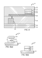
- FIG. 1( a ) shows a cross-section of a thin film transistor ( 100 ) comprising a substrate ( 110 ), a surface ( 120 ) with topography and a conformal layer or coating comprising SiN x applied by chemical vapor deposition (CVD).
- CVD chemical vapor deposition
- FIG. 1( b ) shows a cross-section of a thin film transistor ( 105 ) comprising a substrate ( 110 ) and a surface ( 120 ) with topography and a planarizing layer ( 140 ).
- FIG. 2 shows the cross section of a typical thin film transistor device ( 200 ) in which a contemplated formulation is used as a gate dielectric ( 230 ).
- FIG. 3 shows a contemplated device ( 300 ) where the surface is planarized using the contemplated formulation ( 320 ).
- FIG. 4( a ) shows the cross-section of a typical color filter.
- FIG. 4( b ) shows how contemplated materials are used in a color filter.
- FIG. 5 shows the cross section of an active matrix organic light emitting diode (AMOLED) ( 500 ).
- AMOLED active matrix organic light emitting diode
- FIGS. 6( a ) and 6 ( b ) show schematic cross-sections of a contemplated LED ( 601 ) and the breakout of a contemplated LED ( 600 ), wherein the compositions contemplated herein may be utilized on top of the LED in top-emitting LEDs or on the substrate at the bottom for the bottom emitting LEDs (not shown).
- FIGS. 7( a ) and 7 ( b ) show contemplated flexible substrates. These substrates ( 710 ) are in general rough (roughness of the order of a few hundred nanometers) as shown in the figure.
- FIG. 8 shows a typical cross section of a solar cell ( 800 ).
- FIG. 9 shows an X-ray detector ( 900 ), which comprises a sensor (photoconductor), capacitor and an active matrix thin film transistor addressing unit.
- FIG. 10 shows a typical post-bake spin curve for Example 4.
- FIG. 11 shows a contemplated curing profile for a 300° C. cure.
- FIGS. 12 and 13 show respectively the weight loss of 230° C. and 300° C. cured material.
- FIG. 13A shows Table 1, which shows the cumulative weight loss after ramp and after 1, 2 and 3 hours of holding at a cure temperature.
- FIG. 14 shows a schematic depiction of a micrograph, where the surface is planarized by the contemplated material.
- FIG. 15 shows a cross-section of the organic TFT (OTFT) ( 1500 ) fabricated to test the contemplated material as gate dielectric.
- OTFT organic TFT
- FIG. 15A shows Table 2, which shows the annealing conditions for the semiconductor of Example 5.
- FIGS. 16( a ) and ( b ) show the device characteristics of OTFT.
- FIG. 17 shows the transmittance of the phenylsiloxane-based material and HKLR-based material with respect to glass in the visible optical wavelength range from 400 to 1000 nm.
- FIGS. 18A-18K show spin curces for PTS-series materials obtained by spin coating of the formulations on silicon wafers.
- FIG. 19 shows the outgassing profile of a 250 C-cured HKLR-based material film and the outgassing profile of a 400 C cured phenylsiloxane-based film.
- FIG. 19A shows Table 13, which shows contemplated compositions and their film properties.
- FIG. 19B shows Table 14, which shows the processes for producing layers and then films of several of the contemplated compositions.
- FIG. 19C shows Table 15, and FIG. 19D shows Table 16, which show the PRS 2000 resistance for a continuous six minute exposure at 70 C.
- FIG. 19E shows Table 17, which shows a collection of electrical properties monitored for these compositions.
- FIG. 20 shows the TDMS profile for GR908F.
- FIG. 21 shows the TDMS profile for GR 150F.
- FIG. 22 shows the TGA analysis for GR908F.
- FIG. 23 shows the TGA analysis for GR150F.
- FIG. 23A shows Table 18, which shows a collection of required properties for display dielectrics.
- FIG. 23B shows Table 19, which shows the comparison of the properties for each of the three contemplated materials reviewed for this example.
- FIG. 23C shows Table 20, which shows physical properties of films produced using the contemplated materials on 8′′ wafers.
- FIG. 24 shows the viscosity of contemplated formulations.
- FIG. 25 shows the transmittance of the films from the materials utilized in this example.
- FIG. 25A shows Table 21, which shows the “n” and “k” measurements of the materials.
- FIG. 25C shows Table 23, which shows moisture resistance data using a similar procedure as that in Example 6.
- FIG. 25D shows Table 24, and FIG. 25E shows Table 25, which show shelf life data for the formulations described in Example 9.
- FIG. 25F shows Table 26, which shows the processes for producing layers and then films of each of these compositions.
- FIG. 25G shows Table 27, which shows the PRS 2000 resistance for a continuous exposure of at least 30 minutes at 70° C.
- FIG. 25H shows Table 28A, which shows a collection of electrical properties monitored for these compositions.
- FIGS. 26 and 27 show the results of the TGA experiments, where FIG. 26 is a control composition comprising no surfactants and FIG. 27 shows the composition comprising surfactant.
- FIG. 28 shows the TDMS profile for the control
- FIG. 29 shows the TDMS profile for the surfactant-containing composition.
- FIG. 28A shows Table 28B, which shows a series of shelf-life studies for the surfactant-containing compositions.
- FIG. 28B shows Table 29, which shows the GPC data that indicates molecular weight growth for these materials.
- FIG. 30 shows FTIR data for several contemplated compositions.
- compositions have been developed and utilized in such a manner that can satisfy one or more of the following: a) serve several different functions, including as a passivation layer, a color filter planarizing overcoat, an OLED moisture barrier coating and adhesive, and a film and/or layer in flat panel displays and transistors; b) adequately gap fill in narrow trenches and channels; c) be formed using conventional structural and solvent constituents; d) withstand incorporation of other composition-modifying constituents, such as surfactants and adhesion promoters; e) planarize a surface or substrate to form a component that can be easily incorporated into an optoelectronic application; and/or f) be laid down in ultra-thin, thin and thicker films for multiple applications.
- Contemplated crosslinkable compositions comprise at least one silicon-based compound, at least one catalyst, and at least one solvent. These compositions may also comprise at least one surfactant, at least one crosslinking agent, at least one adhesion promoter, at least one other additive or a combination thereof. Contemplated crosslinkable compositions are applied to suitable surfaces depending on the projected end-use of the coating, layer or film. The at least one catalyst is activated at a suitable point in the production of the layered material, device, film or display, thereby forming the light-transmissive film or layer.
- Optoelectronic devices are also contemplated herein utilizing the above compositions to form a film, layer or coating as part of the device or apparatus.
- the optoelectronic device may comprise one or more light-transmissive films, coatings or layers, such as those described herein, and those light-transmissive films or layer may comprise the same chemical composition or one that is slightly different from another light-transmissive film or layer.
- contemplated optoelectronic devices comprise a surface within the device, and at least one sufficiently light-transmissive crosslinked film, wherein the film is formed from at least one silicon-based material, at least one catalyst, and at least one solvent.
- Optoelectronic devices may also comprise a surface within the device, and at least one sufficiently light-transmissive crosslinkable composition, wherein the composition comprises at least one silicon-based material, at least one crosslinking agent and at least one solvent.
- Contemplated optoelectronic devices comprise a transistor, a light-emitting diode, a color filter, a stainless steel or plastic surface, a photovoltaic cell, a flat panel display, x-ray detectors or a combination thereof.
- Contemplated devices comprise an active matrix thin film organic light emitting display, a passive matrix organic light emitting display, an active matrix thin film transistor liquid crystal display, an electrophoretic display or a combination thereof.
- Contemplated transistors comprise an amorphous silicon thin film transistor, a low temperature polysilicon transistor, an organic transistor, an organic field effect transistor, a static induction transistor, a crystalline silicon transistor or a combination thereof.
- the light-transmissive film forms a passivation layer, a planarization layer or a combination thereof.
- compositions comprise at least one silicon-based compound.
- silicon-based compounds comprise siloxane, silsesquioxane, polysiloxane, polysilsesquioxane, or silazane compounds, such as methylsiloxane, methylsilsesquioxane, phenylsiloxane, phenylsilsesquioxane, methylphenylsiloxane, methylphenylsilsesquioxane, silazane polymers, dimethylsiloxane, diphenylsiloxane, methylphenylsiloxane, polyphenylsilsesquioxane, polyphenylsiloxane, polymethylphenylsiloxane, polymethylphenylsilsesquioxane, polymethylsiloxane, polymethylsilsesquioxane, silicate poly
- a contemplated silazane polymer is perhydrosilazane, which has a “transparent” polymer backbone.
- Contemplated compounds and materials are those that do not meaningfully absorb in the visible range, such as between 400 nm and 800 nm.
- the at least one silicon-based compound comprises polyphenylsilsesquioxane, polyphenylsiloxane, phenylsiloxane, phenylsilsesquioxane, methylphenylsiloxane, methylphenylsilsesquioxane, polymethylphenylsiloxane, polymethylphenylsilsesquioxane, polymethylsiloxane, polymethylsilsesquioxane or a combination thereof.
- contemplated silicon-based compounds comprise both alkyl and aryl constituents, such as methylphenylsilsesquioxane, methylphenylsiloxane, polymethylphenylsiloxane or polymethylphenylsilsesquioxane, wherein the alkyl concentration is varied between a low percentage and a higher percentage—depending on the application—where the total carbon in the compound is represented as the percent of carbon in each type of carbon-based entity.
- a “carbon-based entity” is understood to mean an alkyl group, an aryl group or an aromatic group.
- the percent of carbon represented as alkyl groups is less than about 20% compared with the percent of carbon represented as aryl groups, which is greater than about 80% of the total carbon in the compound. In some embodiments, the percent of carbon represented as alkyl groups may be less than about 10% compared with the percent of carbon represented as aryl groups, which is greater than about 90% of the total carbon in the compound.
- the percent of carbon that is represented as alkyl groups is greater than about 20% compared with the percent of carbon that is represented as aryl groups, which is less than about 80% of the total carbon in the compound. In some embodiments, the percent of carbon that is represented as alkyl groups is greater than about 30% compared with the percent of carbon that is represented as aryl groups, which is less than about 70% of the total carbon in the compound.
- an integrated LKHR-based material may be resistant to less aggressive photoresist strippers
- an integrated HKLR-based material may be resistant to both less and more aggressive photoresist strippers.
- the term “integrated” means that the substituents are integrated onto one compound, such as the methylphenylsilsesquioxane.
- compounds are “blended”, wherein the substituents are found on different compounds, and the compounds are then blended or mixed to produce a material.
- An example of blending is to incorporate a methylsiloxane or methylsilsesquioxane with a phenylsiloxane or phenylsilsesquioxane.
- Some contemplated silicon-based compounds include compositions formed from hydrolysis-condensation reactions of at least one reactant having the formula: R 1 x Si(OR 2 ) y , where R 1 is an alkyl, alkenyl, aryl, or aralkyl group, and x is an integer between 0 and 2, and where R 2 is a alkyl group or acyl group and y is an integer between 0 and 2.
- R 1 x Si(OR 2 ) y where R 1 is an alkyl, alkenyl, aryl, or aralkyl group, and x is an integer between 0 and 2, and where R 2 is a alkyl group or acyl group and y is an integer between 0 and 2.
- Materials also contemplated include silsequioxane polymers of the general formula (C 6 H 5 SiO 1.5 ) x , where x is an integer greater than about 4.
- silicon-based compounds include siloxane polymers, copolymers and blockpolymers, hydrogensiloxane polymers of the general formula (H 0-1.0 SiO 1.5-2.0 ) x , hydrogensilsesquioxane polymers, which have the formula (HSiO 1.5 ) x , where x is greater than about four and derivatives of silicic acid and combinations thereof. Also included are copolymers of hydrogensilsesquioxane and an alkoxyhydridosiloxane or hydroxyhydridosiloxane.
- Organosiloxane polymers acrylic siloxane polymers, silsesquioxane-based polymers, derivatives of silicic acid, organohydridosiloxane polymers of the general formula (H 0-1.0 SiO 1.5-2.0 ) n (R 0-1.0 SiO 1.5-2.0 ) m , and organohydridosilsesquioxane polymers of the general formula (HSiO 1.5 ) n (RSiO 1.5 ) m , where m is greater than zero and the sum of n and m is greater than about four and R is alkyl or aryl, and combinations thereof.
- Some useful organohydridosiloxane polymers have the sum of n and m from about four to about 5000 where R is a C 1 -C 20 alkyl group or a C 6 -C 12 aryl group.
- Some specific examples include alkylhydridosiloxanes, such as methylhydridosiloxanes, ethylhydridosiloxanes, propylhydridosiloxanes, t-butylhydridosiloxanes, phenylhydridosiloxanes; and alkylhydridosilsesquioxanes, such as methylhydridosilsesquioxanes, ethylhydridosilsesquioxanes, propylhydridosilsesquioxanes, t-butylhydridosilsequioxanes, phenylhydridosilsesquioxanes and combinations thereof.
- specific organohydridosiloxane resins utilized herein have the following general formulas: [H—Si 1.5 ] n [R—SiO 1.5 ] m Formula (1) [H 0.5 —Si 1.5-1.8 ] n [R 0.5-1.0 —SiO 1.5-1.8 ] m Formula (2) [H 0-1.0 —Si 1.5 ] n [R—SiO 1.5 ] m Formula (3) [H—Si 1.5 ] x [R—SiO 1.5 ] y [SiO 2 ] z Formula (4) wherein: the sum of n and m, or the sum or x, y and z is from about 8 to about 5000; R is is selected from substituted and unsubstituted, normal and branched alkyls (methyl, ethyl, butyl, propyl, pentyl), alkenyl groups (vinyl, allyl, isopropenyl), cycloalkyls,
- Silica compounds contemplated herein are those compounds found in U.S. Pat. Nos. 6,022,812; 6,037,275; 6,042,994; 6,048,804; 6,090,448; 6,126,733; 6,140,254; 6,204,202; 6,208,041; 6,318,124 and 6,319,855.
- At least one catalyst may be added to the at least one silicon-based compound.
- suitable catalysts are heat-activated catalysts.
- the term “catalyst” means any substance that affects the rate of the chemical reaction by lowering the activation energy for the chemical reaction. In some cases, the catalyst will lower the activation energy of a chemical reaction without itself being consumed or undergoing a chemical change.
- These condensation catalysts are often only activated at a particular temperature, such as an elevated temperature. Thus, at one temperature (such as room temperature) the composition maintains a low molecular weight, thus enabling good planarization ability over a surface.
- Contemplated condensation catalysts comprise those catalysts that can aid in maintaining a stable silicate solution.
- Contemplated metal-ion-free catalysts may comprise onium compounds and nucleophiles.
- the catalyst may be, for example an ammonium compound (such as quaternary ammonium salts), an amine, a phosphonium compound or a phosphine compound.
- contemplated catalysts include those catalysts that are relatively molecularly “small” or that produce relatively small cations, such as quaternary ammonium salts.
- contemplated catalysts include tetramethylammonium acetate (TMAA), tetramethylammonium hydroxide (TMAH), tetrabutylammonium acetate (TBAA), cetyltrimethylammonium acetate (CTAA), tetramethylammonium nitrate (TMAN), other ammonium-based catalysts, amine-based and/or amine-generating catalysts and combinations thereof.
- TMAN is used and can be obtained by either dissolving TMAN in water or by converting TMAA or TMAH to TMAN by using nitric acid.
- catalysts include (carboxymethyl)trimethylammonium chloride, (carboxymethyl)trimethylammonium hydroxide, (carboxymethyl)trimethylammonium formate and (carboxymethyl)trimethylammonium acetate.
- (carboxymethyl)trimethylammonium” is also known as “Betaine”. Advantages provided by utilizing betaine are: improved catalytic activity, low toxicity, and it eliminates the ionic species (residual ions can promote “image sticking” in some applications).
- At least one solvent is added to the at least one silicon-based compound and the at least one catalyst.
- Contemplated solvents include any suitable pure or mixture of organic molecules that are volatilized at a desired temperature and/or easily solvates the components discussed herein.
- the solvent may also comprise any suitable pure or mixture of polar and non-polar compounds.
- pure means that component that has a constant composition. For example, pure water is composed solely of H 2 O.
- mixture means that component that is not pure, including salt water.
- polar means that characteristic of a molecule or compound that creates an unequal charge, partial charge or spontaneous charge distribution at one point of or along the molecule or compound.
- non-polar means that characteristic of a molecule or compound that creates an equal charge, partial charge or spontaneous charge distribution at one point of or along the molecule or compound.
- Contemplated solvents are also those solvents that can, alone or in combination, modify the viscosity, intermolecular forces and surface energy of the solution in order to, in some cases, improve the gap-filling and planarization properties of the composition. It should be understood, however, that suitable solvents may be those solvents that influence the profile of the composition in other ways, such as by influencing the crosslinking efficiency, influencing the thermal stability, influencing the viscosity, and/or influencing the adhesion of the resulting layer or film to other layers, substrates or surfaces.
- the at least one solvent may comprise those solvents that are considered part of the hydrocarbon family of solvents.
- Hydrocarbon solvents are those solvents that comprise carbon and hydrogen. It should be understood that a majority of hydrocarbon solvents are non-polar; however, there are a few hydrocarbon solvents that could be considered polar. Hydrocarbon solvents are generally broken down into three classes: aliphatic, cyclic and aromatic. Aliphatic hydrocarbon solvents may comprise both straight-chain compounds and compounds that are branched and possibly crosslinked, however, aliphatic hydrocarbon solvents are not considered cyclic. Cyclic hydrocarbon solvents are those solvents that comprise at least three carbon atoms oriented in a ring structure with properties similar to aliphatic hydrocarbon solvents.
- Aromatic hydrocarbon solvents are those solvents that comprise generally three or more unsaturated bonds with a single ring or multiple rings attached by a common bond and/or multiple rings fused together.
- Contemplated hydrocarbon solvents include toluene, xylene, p-xylene, m-xylene, mesitylene, solvent naphtha H, solvent naphtha A, alkanes, such as pentane, hexane, isohexane, heptane, nonane, octane, dodecane, 2-methylbutane, hexadecane, tridecane, pentadecane, cyclopentane, 2,2,4-trimethylpentane, petroleum ethers, halogenated hydrocarbons, such as chlorinated hydrocarbons, nitrated hydrocarbons, benzene, 1,2-dimethylbenzene, 1,2,4-trimethylbenzene, mineral spirits, kerosine, isobut
- the at least one solvent may comprise those solvents that are not considered part of the hydrocarbon solvent family of compounds, such as ketones, such as acetone, diethyl ketone, methyl ethyl ketone and the like, alcohols, esters, ethers and amines.
- Other contemplated solvents include ethyl lactate, propylene glycol monomethyl ether acetate (PGMEA) or a combination thereof.
- the at least one solvent may comprise a combination of any of the solvents mentioned herein.
- the at least one solvent may be present in solution in an amount less than about 90% by weight. In some embodiments, at least one solvent may be present in solution in an amount from about 50 to 90% by weight. In other embodiments, at least one solvent may be present in solution in an amount from about 55 to 85% by weight. In yet other embodiments, at least one solvent may be present in solution in an amount from about 65 to 85% by weight.
- the determination of what is the appropriate amount of solvent to add to composition depends on a number of factors, including: a) thicknesses of the desired layers or films, b) desired concentration of the solids in the composition, c) application technique of the composition and/or d) spin speeds, when spin-coating techniques are utilized.
- Spin and spray coaters can handle compositions with low viscosity (i.e. 3 centipoises), but slot die or slit coaters often need compositions having a high viscosity.
- the solid content should be increased (or reduce solvent amount) to get viscous material—i.e. 9 centipoises.
- the viscous formulation or formulation with higher solid content will give thicker film (>2 ⁇ m).
- the solvents used herein may comprise any suitable impurity level.
- the solvents utilized have a relatively low level of impurities, such as less than about 1 ppm, less than about 100 ppb, less than about 10 ppb, less than about 1 ppb, less than about 100 ppt, less than about 10 ppt and in some cases, less than about 1 ppt.
- These solvents may be purchased having impurity levels that are appropriate for use in these contemplated applications or may need to be further purified to remove additional impurities and to reach the less than about 10 ppb, less than about 1 ppb, less than about 100 ppt or lower levels that suitable and/or desired.
- compositions may further comprise at least one composition-modifying constituent, such as at least one surfactant, at least one adhesion promoter, at least one crosslinking agent, at least one other additive or a combination thereof.
- composition-modifying constituents are designed to influence the properties of the compositions, coatings, layers and/or films. Contemplated properties which may be influenced, are surface tension, adhesion to other layers or surfaces, viscosity, density, transmittance/transparency or a combination thereof.
- At least one surfactant is considered to be one of the contemplated composition-modifying constituents.
- Surfactants may be added to lower surface tension.
- the term “surfactant” means any compound that reduces the surface tension when dissolved in H 2 O or other liquids, or which reduces interfacial tension between two liquids, or between a liquid and a solid.
- Contemplated surfactants may include at least one anionic surfactant, cationic surfactant, non-ionic surfactant, Zwitterionic surfactant or a combination thereof.
- the surfactant may be dissolved directly into the composition or may be added with one of the compositions components (the at least one silicon-based compound, the at least one catalyst, the at least one solvent) before forming the final composition.
- Contemplated surfactants may include: polyether modified polydimethylsiloxanes such as BYK 307 (polyether modified poly-dimethyl-siloxane, BYK-Chemie), sulfonates such as dodecylbenzene sulfonate, tetrapropylenebenzene sulfonate, dodecylbenzene sulfonate, a fluorinated anionic surfactant such as Fluorad FC-93, and L-18691 (3M), fluorinated nonionic surfactants such as FC-4430 (3M), FC-4432 (3M), and L-18242 (3M), quaternary amines, such as dodecyltrimethylammonium bromide or cetyltrimethylammonium bromide, alkyl phenoxy polyethylene oxide alcohols, alkyl phenoxy polyglycidols, acetylinic alcohols, polyglycol ethers such as Tergitol
- the at least one surfactant may be present in solution in an amount less than about 1% by weight. In some embodiments, the at least one surfactant may be present in solution in an amount from about 0.001% to about 1% by weight. In other embodiments, the at least one surfactant may be present in solution in an amount from about 0.001% to about 0.25% by weight. In some embodiments, at least two surfactant constituents may be present in solution. The determination of what is the appropriate amount of a composition-modifying constituent to add to composition depends on a number of factors, including: a) minimizing defects in the film, and/or b) balancing the film between good adhesion and desirable film properties.
- At least one adhesion promoter may be added to the composition, alone or with the at least one surfactant, in order to influence the ability of the layer, coating or film to adhere to surrounding substrates, layers, coatings, films and/or surfaces.
- the at least one adhesion promoter comprises at least one of the following characteristics: a) is thermally stable after heat treatment, such as baking, at temperatures generally used for optoelectronic component manufacture, and/or b) can surprisingly act as an adhesion promoter by promoting electrostatic and coulombic interactions between layers of materials, as well as promoting understood Van derWaals interactions in some embodiments.
- the addition of at least one adhesion promoter such as at least one weak acid/weak base, at least one weak acid/strong base, at least one strong acid/strong base, at least one strong acid/weak base, at least one amine base, at least one amine salt or a combination thereof increases the electrostatic and coulombic interaction.
- at least one adhesion promoter such as at least one weak acid/weak base, at least one weak acid/strong base, at least one strong acid/strong base, at least one strong acid/weak base, at least one amine base, at least one amine salt or a combination thereof increases the electrostatic and coulombic interaction.
- Contemplated adhesion promoters include aminopropyl triethoxysilane (APTEOS) nitrate, APTEOS acetate, APTEOS sulfonate, APTEOS methanesulfonate, APTEOS triflate, APTEOS tosylate, APTEOS nonafluorobutane-1-sulfonate (nfbs) or any other amine salt or combination of amine salts, Suitable amine bases comprise ammonium, pyridine, aniline, TMAH, CTAH, TBAH, APTEOS or a combination thereof.
- APTEOS aminopropyl triethoxysilane
- adhesion promoters include 3-(triethoxysilyl)propylsuccininc anhydride, dimethyldihydroxy silane, methylphenyl dihydroxysilane or combinations thereof.
- the at least one adhesion promoter may be present in solution in an amount less than about 20% by weight. In some embodiments, the at least one adhesion promoter may be present in solution in an amount from about 0.001% to about 20% by weight. In other embodiments, the at least one adhesion promoter may be present in solution in an amount from about 0.26% to about 2.6% by weight. In some embodiments, at least two adhesion promoters may be present in solution.
- At least one crosslinking agent may be added to the composition.
- crosslinking refers to a process in which at least two molecules, or two portions of a long molecule, are joined together by a chemical interaction or reaction. Such interactions may occur in many different ways including formation of a covalent bond, formation of hydrogen bonds, hydrophobic, hydrophilic, ionic or electrostatic interaction.
- molecular interaction may also be characterized by an at least temporary physical connection between a molecule and itself or between two or more molecules. The chemical reaction may take place between two identical, or non-identical reactive groups, which may be located on the same or on two separate backbones.
- the reactive groups may react with one or more than one exogenous crosslinking molecules to crosslink the at least one silicon-based polymer. It should be understood that while the at least one catalyst lowers the activation energy of the composition in order to effect crosslinking of the at least one silicon-based compound, the at least one crosslinking agent may be added in order to continue crosslinking the at least one silicon-based compound in order to increase the crosslinking density of the coating, layer or film.
- compositions, coatings, films, layers or combination thereof it may be beneficial to either lower or increase one or both the viscosity and the intermolecular forces constituent in order to optimize the gap-filling and planarization properties for the particular end use.
- One method used to modify the planarization composition is to modify and/or replace the at least one solvent, wherein the at least one solvent is compatible with the at least one silicon-based compound and modifies at least one of the intermolecular forces or surface forces components of the planarization composition to which it is added.
- Another method is to add at least one composition-modifying constituent, such as those mentioned herein.
- intermolecular forces means those bonding or non-bonding forces, such as Van der Waals, electrostatic, steric, coulombic, hydrogen bonding, ionic, covalent, dipole-dipole, dispersion, magnetic attraction and combinations thereof, that take place between two or more parts of matter or components, such as a planarization composition and a surface, a planarization composition and another layer of material, molecules that make up the planarization composition and combinations thereof.
- the at least one solvent, the at least one composition-modifying constituent or a combination thereof modifies the apparent viscosity by at least about 10%. In other contemplated embodiments, the apparent viscosity is modified by at least about 20%. In yet other contemplated embodiments, the apparent viscosity is modified by at least about 30%.
- apparent viscosity means the characteristic of fluid's internal resistance to flow and which equals the ratio of stress to the rate of strain. In micron and submicron trenches, the apparent viscosity represents the integral effect of surface forces and usually decreases from the nominal viscosity due to the size effect where the ratio between surface force and body force is large.
- nominal viscosity means that viscosity that is the bulk fluid property determined from a commercially available viscometer, such as a Brookfield viscometer, and is calculated from measurements of forces and velocities when liquid is Newtonian.
- a surface forces component such as an interfacial surface tension
- Solvents and composition-modifying constituents contemplated herein can modify the interfacial surface tension by at least about 10% when compared to a conventional planarization composition known to one of ordinary skill in the art of layered materials.
- the at least one solvent, the at least one composition-modifying constituent or combination thereof can modify the interfacial surface tension by at least about 20% when compared to a conventional planarization composition.
- the at least one solvent, the at least one composition-modifying constituent or combination thereof can modify the interfacial surface tension by at least about 30% when compared to a conventional planarization composition.
- a silicon-based compound such as a phenylsilsesquioxane oligomer-containing formulation
- a silicon substrate is applied to a silicon substrate and cured to form a polymer film.
- the phenylsilsesquioxane oligomer has a molecular weight of 500-2500 AMU.
- contemplated phenylsilsesquioxane oligomers have a molecular weight of 700-2100 AMU.
- contemplated phenylsilsesquioxane oligomers have a molecular weight of 800-1900 AMU.
- the formulation can be prepared by dissolving the phenylsilsesquioxane oligomer into propylene glycol monomethyl ether acetate (PGMEA) in an amount varying between 15 and 45 percent by weight.
- a condensation catalyst tetramethylammonium nitrate
- a surfactant such as BYK 307 from BYK-Chemie
- the formulation is then applied to the substrate by spinning, slot die coating, dipping, or spraying.
- the film is formed on the substrate by baking between 150 and 300° C. to remove solvent, followed by a curing step of between 150 and 400° C.
- the thickness of the resulting film varies between 0.3 and 2.5 um, depending on the weight percent phenylsilsesquioxane content of the formulation.
- Film properties include low outgassing, good planarization, high optical transparency, high thermal stability, high refractive index and good electrical insulation (k ⁇ 3). These properties are desirable for use in various optoelectronic applications, such as flat panel displays.
- Contemplated materials, coatings, layers and/or films may have a relatively high refractive index. In some embodiments, the refractive index is greater than about 1.5.
- Optoelectronic devices comprising at least one light-transmissive film or layer produced by providing at least one silicon-based compound, providing at least one catalyst, providing at least one solvent, blending the at least one silicon-based compound, the at least one catalyst and the at least one solvent to form a composition, applying the composition to a suitable surface, and at least partially activating the at least one catalyst in order to form the light-transmissive film or layer.
- an optoelectronic device may comprise one or more light-transmissive films or layers, such as those described herein, and those light-transmissive films or layer may comprise the same chemical composition or one that is slightly different from another light-transmissive film or layer.
- at least one composition-modifying constituent may be added to the composition.
- Contemplated compositions are applied to suitable surfaces, such as layers, films or substrates depending on the projected end-use of the film formed from the composition.
- Contemplated films are, in some embodiments, etch resistant to at least one aggressive etch chemistry.
- photoresist strippers (those that are used to remove photoresist after using it for etching the dielectric or metal) are chosen to achieve a high etch rate of the order of 3000 A/min or higher, which can be considered an aggressive etch chemistry.
- photoresist stripping temperature is high of the order of 50 C or above.
- compositions described herein comprising primarily aryl moieties, such as phenyl, are soluble in photoresist strippers at temperatures above 40 C.
- Surfaces contemplated herein may comprise any desirable substantially solid material, such as a glass, stainless steel or plastic substrate found in the optoelectronic manufacturing industry.
- the surfaces may be coated or uncoated, patterned or unpatterned, and may reside anywhere in the optoelectronic device, such as on the top of a TFT structure, between or in TFT structures, on top of a stainless steel or plastic substrate above which TFT or any suitable semiconductor device structures (or other structures) are placed, adjacent a color filter in an LCD, adjacent an OLED device, adjacent an electrophoretic device or adjacent any other surface within a flat panel or other display or optoelectronic device.
- Some contemplated surfaces comprise a non-planar surface topography and other contemplated surfaces that have already been planarized.
- Particularly desirable surfaces comprise films, glass, ceramic, plastic, metal or coated metal, or composite material. Surfaces comprise at least one layer and in some instances comprise a plurality of layers. In other embodiments, the surface comprises a material common in the optoelectronic industries. Suitable surfaces contemplated herein may also include another previously formed layered stack, other layered component, or other component altogether.
- the at least one catalyst is activated at a suitable point in the production of the layered material, device, film or display, thereby forming the light-transmissive film or layer.
- the composition is applied to a suitable surface and the at least one catalyst is at least partially activated.
- the at least one catalyst may be activated in that it converts the composition to a partially crosslinked gelled film, but has not been activated as such to convert the composition to a fully crosslinked film.
- the composition is at least partially activated before application to a surface, substrate, layer or film.
- the composition is applied to a suitable surface, layer, film or substrate and the at least one catalyst is fully activated thus resulting in a crosslinked and dense film or layer.
- Contemplated catalysts may be activated by any suitable device, method or action, including by applying heat, light, vibration or another chemical compound.
- compositions contemplated herein may be coated onto a surface by any suitable method, including continuous deposition techniques such as spin coating, gravure coating, curtain coating, dip coating, slot-die coating, spray coating, and continuous nozzle coating; and discontinuous deposition techniques such as ink jet printing, gravure printing, and screen printing.
- continuous deposition techniques such as spin coating, gravure coating, curtain coating, dip coating, slot-die coating, spray coating, and continuous nozzle coating
- discontinuous deposition techniques such as ink jet printing, gravure printing, and screen printing.
- compositions where the composition comprises at least one sufficiently light-transmissive crosslinkable composition, wherein the composition comprises at least one silicon-based material, at least one crosslinking agent and at least one solvent, the composition after a cure or curing step having at least one cure temperature and at least one cure time has a weight loss of less than about 2% during further processing at or below the cure temperature. In other embodiments, this weight loss is less than about 1%.
- the at least one cure temperature ranges from about 150° C. to about 400° C., and the at least one cure time is less than about 2 hours.
- the films produced by the compositions and processes described herein may have one or more advantages over those previously known to the art, including improved dielectric breakdown strength also known as electric field to breakdown (FBD), which enables the film to be used in optoelectronic applications.
- BBD electric field to breakdown
- gate dielectrics, planarization layers and passivation layers may need to have a FBD of at least about 2.5 MV/cm, and in some embodiments, greater breakdown fields are desirable.
- a transparency to light in the range of about 400 nm to about 800 nm of at least about 90% is desirable in contemplated films.
- the films, coatings and layers have a transparency to light of at least about 95%.
- the films, coatings and layers have a transparency to light of at least about 98%. In other embodiments, the films, coatings and layers have a transparency to light of at least about 99%. In some embodiments, the films, coatings and layers have a degree of planarization of above 90% over topographies. In other embodiments, the films, coatings and layers have root mean square surface roughness lower than 10 nm or Angstroms.
- conformal coatings are used as insulators for an interlayer dielectric, such as CVD SiO 2 and SiN.
- a planarizing/gap filling material is desirable as it avoids sharp corners that can create shorts in subsequent metallization steps.
- SiN/SiO 2 can also be used, but using a planarizing material increases the area of the pixel electrode and therefore increases the brightness of the display.
- organic materials are used, such as benzocyclobutene (BCB) or a photoimageable acrylic.
- BCB benzocyclobutene
- materials disclosed herein have a higher thermal stability.
- materials disclosed herein have a higher thermal stability, and also have higher transparency. High thermal stability is often very desirable, as it prevents outgassing that can cause adhesion problems as well as damage moisture sensitive components in the finished device.
- TFTs Thin Film Transistors
- compositions, coatings, materials, films and layers disclosed herein may be used as interlevel (between 1 st and second metal layers, or between second metal and pixel electrode layer) or intralevel (between metal lines or contacts in the same level) dielectric (ILD) layers in thin film transistors, such as amorphous silicon thin film transistors, low temperature polysilicon transistors, crystalline silicon transistors, organic transistors, organic field effect transistors or static induction transistors.
- ILD interlevel dielectric
- compositions may also replace the insulator (known as gate dielectric and the material commonly used in current devices is SiN) above the gate.
- the contemplated compositions, films and/or layers may also function as passivation layers and planarization layers in these devices.
- Planarizing layer differs from conformal layers such as chemical vapor deposited silicon nitride in thickness variation across the surface as shown in FIGS. 1( a ) and 1 ( b ).
- FIG. 1( a ) shows a cross-section of a conformal coated patterned substrate ( 100 ) comprising a substrate ( 110 ), a surface ( 120 ) with topography and a conformal layer or coating comprising SiN x applied by chemical vapor deposition (CVD).
- Conformal layers ( 130 ) give rise to uniform thickness ( 135 ) all over the surface ( 120 ) thereby keeping the topography of the surface ( 120 ) intact as shown in FIG. 1( a ).
- FIG. 1( a ) shows a cross-section of a conformal coated patterned substrate ( 100 ) comprising a substrate ( 110 ), a surface ( 120 ) with topography and a conformal layer or coating comprising SiN x applied by chemical vapor deposition (CVD).
- FIG. 1( b ) shows a cross-section of a planarized substrate ( 105 ) comprising a substrate ( 110 ) and a surface ( 120 ) with topography and a planarizing layer ( 140 ), Planarizing layers give rise to different thicknesses in different regions (lower thickness on top of hills and higher thickness in the valleys) such that the topography of the surface is altered and the surface becomes almost flat as shown in FIG. 1( b ).
- the degree of planarization (DOP, expressed in percentage) is the difference between the initial height of the feature on a given surface before coating ( 150 ) and the dip ( 160 ) in the planarizing coating (from the top surface of coating) at the valley region normalized to the initial height of the feature.
- DOP is represented by this ratio (1 ⁇ (x ⁇ y)/x ⁇ ) and is expressed as a percentage. Layers that yield greater than 90% DOP are considered to be good planarizing layers. Usually the amount of solid or resin content in the formulation or the amount of solvent is adjusted, or the solvent(s) is(are) changed to achieve a flat surface for a given topography.
- FIG. 2 shows the cross section of a typical thin film transistor device ( 200 ) in which a contemplated formulation is used as a gate dielectric ( 230 ).
- the substrate ( 210 ) could be glass, plastic or metal.
- a metal layer is formed on the top of a substrate ( 210 ) usually by physical vapor deposition process (such as sputtering) and patterned to form the gate metal ( 220 ).
- the gate dielectric material ( 230 ) planarizes the surface topography as shown in FIG. 2 .
- amorphous silicon ( 240 ) is deposited on top of the gate dielectric. Source and drain regions in a-Si are doped with n+ to achieve a low contact resistance. The source ( 270 ) and drain ( 260 ) contacts are formed on the n+ doped ( 250 ) regions of amorphous silicon ( 240 ). In general, whenever a planarizing layer is used, the surface topography is largely reduced.
- a contemplated device ( 300 ) after building the TFT regions ( 330 ) on a substrate ( 310 ), the surface is planarized using the contemplated formulation ( 320 ) as shown in FIG. 3 .
- This layer ( 320 ) is usually known as interlayer dielectric as it exists between the first metal layer ( 340 ) (which also forms the gate in TFT regions) and the pixel electrode ( 350 ).
- the pixel electrode ( 350 ) is connected to the drain (not shown) of the TFT.
- This layer ( 320 ) is also called passivation layer as it protects the TFT regions during further processing steps and it isolates the liquid crystal region from the TFT region.
- LCD liquid crystal display
- the liquid crystal molecules are oriented in different directions to selectively allow (or block) light passage and thereby achieve image displaying.
- the color to the image is imparted by the color filter screen.
- a color filter screen is a contemplated end use for the compositions, layers and films disclosed herein.
- FIG. 4( a ) shows the cross section of a typical color filter and FIG. 4( b ) shows how contemplated materials are used in a color filter.
- a color filter screen in a LCD is fabricated by first depositing a chromium-based or resin-based black matrix ( 420 ) on a substrate ( 410 ) and patterning it. This step is followed by forming three primary color regions ( 430 , 432 , 434 ) by depositing the respective resins and patterning to define red, green and blue regions.
- ITO indium tin oxide
- the common electrode ( 440 ) follows the topography of the underlying color regions.
- a polyimide layer is deposited on top of the electrode (not shown) to complete the color filter screen. Because of the topography in ITO, differential field results leading to differential response of liquid crystals. ITO deposition is a sputtering process, which may also damage color resins.
- To protect the three primary color regions the surface is covered by an overcoat layer ( 450 ) as shown in FIG. 4( b ).
- This overcoat layer ( 450 ) may comprise contemplated formulations, as described throughout this disclosure. This layer in addition to protecting color regions, planarizes the surface.
- the common electrode ( 440 ) deposited on top of this overcoat is flat and provides a uniform field to the liquid crystal in a given pixel or subpixel.
- contemplated layers, films, materials or composition may be used as a gate dielectric, inter- or intra-level dielectric, passivation and planarization layers in different regions of the TFTLCD and as color filter overcoat in color filter screens.
- OLED Organic Light-Emitting Diode
- FIG. 5 shows the cross section of an active matrix organic light emitting diode (AMOLED) ( 500 ).
- an OLED device comprises a cathode ( 566 ) (usually Ca, Al or Ba), a light emitting polymer and an anode (usually ITO) ( 550 ).
- the light emitting polymer comprises a hole transport layer ( 562 ) to conduct holes and an electron transport layer ( 564 ) to transport electrons. Light is emitted when holes combine with electrons.
- the substrate ( 510 ) is first coated with a moisture barrier layer ( 520 ). The contemplated formulation may be used for this purpose.
- the TFT regions ( 540 ) are formed on the contemplated moisture barrier layer ( 520 ).
- a passivation layer ( 530 ) also called an ILD
- This passivation layer should have moisture and O 2 diffusion barrier properties.
- the contemplated formulation is also deposited on top of OLED region as an encapsulation layer ( 570 ) to prevent moisture and O 2 diffusion from the top and the sides.
- the OLED region needs to be completely encapsulated by such a barrier layer or plurality of barrier layers to prevent diffusion of water, oxygen or other extraneous substances in the environment.
- the diffusion of such species to OLED reduces the lifetime and reliability of OLED devices.
- the contemplated material may be used in general as oxygen and moisture diffusion barrier layers surrounding the OLED regions and in particular as encapsulation above the OLED regions and passivation layer below the anode.
- the contemplated material can also be used as interlayer dielectric to planarize topographies, gate dielectric and passivation layer in TFT regions.
- Light-emitting diodes are two terminal devices with a p and n type semiconductors deposited on sapphire/GaN substrate with an inherent high refractive index.
- the pn junction emits light when biased with a certain voltage.
- FIG. 6 shows a schematic cross-sections of a contemplated LED ( 601 ) and the breakout of a contemplated LED ( 600 ), wherein the compositions contemplated herein may be utilized on top of the LED in top-emitting LEDs or on the substrate at the bottom for the bottom emitting LEDs (not shown).
- the contemplated composition, materials, films and layers are used as a light extraction layer ( 630 and 635 ).
- the contemplated formulation is applied on top of the LED region ( 620 ), which is on top of a substrate layer ( 610 ), as an adhesive to the lens ( 640 ) (usually made of polycarbonate) that goes on top of the LED region ( 620 ).
- This adhesive layer ( 630 and 635 ) is transparent and its refractive index is between the refractive indices of LED layer ( 620 ) and lens layer ( 640 ).
- refractive index matching using this layer the total internal reflection of light back into the LED region is reduced and more of the emitted light from LED is extracted to the lens (or from the substrate to outside in bottom emitting LED device architecture—not shown in figure), which reduces light intensity loss due to total internal reflection and makes the LEDs to have high brightness.
- Contemplated materials, coatings, layers and/or films may have a relatively high refractive index. In some embodiments, the refractive index is greater than about 1.5. These materials, coatings, layers and/or films can also achieve increased thickness without cracking, and have high thermal stability. In some embodiments, the thickness is greater than 1 ⁇ m. In other embodiments, the thickness is greater than about 2.5 ⁇ m.
- the contemplated composition or layer gives rise to thick films with a good adhesion between LED layers, lens and substrate layers.
- PET can go to a maximum temperature of 150 C.
- PEN substrates can go up to 180 C, but they do not work well with LCD, because of birefringence.
- Modified polycarbonates have higher TGs (around 215 C). These plastic films have a refractive index of 1.59.
- the formulation, layers, and films (represented as 730 ) contemplated herein are used to planarize stainless steel, metal foil or plastic where transistors or any other devices would subsequently be built.
- the main functionalities provided by the contemplated material are surface planarization and moisture barrier properties.
- the coatings can be applied to the substrate by Mayer Rod applicators or by any other coating methods mentioned earlier.
- the films are thermal cured at 150 C. for 5 minutes and UV cured at 450 mJ/cm 2 for about 5 seconds.
- the films are generally about 3-4 micrometers in thickness and should provide moisture transmission resistance.
- the initial roughness shows that the films are quite flat—around 2 nm for the roughness or Ra measurement.
- the Ra was shown to be about 0.5 nm.
- a photovoltaic cell converts light to electric current and is the heart of solar cells.
- the cell is constructed with two layers of semiconductors, p- and n-type sandwiched together to form a ‘pn junction’.
- When light is incident on the semiconductor it is absorbed by the semiconductor and the energy is transferred to electrons in the n-type semiconductor which are then able to move through the material.
- a corresponding positive charge carrier or ‘hole’ is created to maintain electrical neutrality.
- the electrons and holes near the pn junction are swept across in opposite directions by the action of the electric field. This separation of charge induces a voltage across the device generating electricity in external circuit.
- a typical cross section of a solar cell ( 800 ) is given in FIG. 8 .
- the incident light is represented by ( 890 ).
- solar cells are built on glass substrates.
- plastic or stainless steel substrates 810 are candidates for substrates.
- the rough surface of these substrates is planarized using the contemplated material ( 820 ) and a back contact ( 830 ) made from metal is added to the layered material.
- p-type and n-type semiconductor materials ( 840 and 850 , respectively) are deposited.
- a thin layer ( 860 ) of antireflective coating is deposited on top of the shiny semiconductor (such as silicon) surface to promote more absorption of the incident light ( 890 ).
- the cell ( 800 ) is finished with a front contact ( 870 ) on top of n-type semiconductor.
- the contemplated material ( 880 ) is deposited on top of the front contact to protect metal regions ( 870 ) from environmental damage.
- an X-ray detector ( 900 ) in general comprises a sensor (photoconductor), capacitor and an active matrix thin film transistor addressing unit.
- the sensor is the photoconductor ( 940 ) that absorbs the incoming x-rays ( 970 ) and creates a corresponding electric charge which gets stored in a capacitor ( 920 ).
- the photoconductor ( 940 ) is coated with contemplated dielectric layers ( 950 ) and then a top electrode ( 960 ).
- the active matrix addressing detects the charge and sends the readout of the signal to external electronics which in turn displays the image.
- Each pixel in the addressing unit contains one addressing transistor ( 930 , TFT).
- the layered material is built on a substrate ( 910 ), which may be glass.
- a thickness of around 300 to 500 ⁇ m is needed to reduce the incident X-ray energy to acceptable level that is not harmful, thin layer of amorphous silicon photoconductor alone cannot achieve this thickness. Therefore, phosphors or photoconductors are used which will convert the incident X-ray (after emerging form object to image) to either light or electron respectively; which in turn will be read out by the amorphous silicon arrays (just like in a flat panel display).
- a scintillating layer typically CsI
- photodiode can be used instead of the photoconductor and capacitor (not shown).
- the materials that are used for the scintillating layer are corrosive, so the contemplated material can be used as a protecting overcoat layer between the TFT's and the scintillating layer.
- the contemplated layers can also be used in TFT layer as gate dielectric, ILD and passivation as described earlier.
- polyphenylsilsesquioxane (GR950F manufactured by TECHNEGLASTM) is dissolved in 70 g of PGMEA. 0.75 g of APTEOS (utilized as an adhesion promoter) is added and the solution is heated to 80° C. After 2 hours the solution is cooled and 0.83 g of glacial acetic acid is added.
- a TMAN solution is prepared by weighing 0.5 g of TMAN (96% powder) and adding 99.5 g of deionized water. This TMAN solution is stirred for 30 minutes at room temperature and stored at room temperature. The silsesquioxoane solution is filtered through 0.1 micron filter and then TMAN is added. The solution can then be used to form a film on a substrate by spin coating or another method.
- dewets refers to film defects caused by poor adhesion which typically appear between film-formation and cure.
- a contemplated composition is prepared which comprises 30 g of phenylsilsesquioxane (GR950F manufactured by TECHNEGLASTM) and is blended with 70 g of PGMEA, along with 0.3333 g of a TMAN solution.
- phenylsilsesquioxane GR950F manufactured by TECHNEGLASTM
- GR950F is a resin flake of >98% phenylsilsesquioxane. It has a MW range of 800-1200 AMU and a melting point of 60° C.
- the 30 g of GR950F is placed in an empty HOPE bottle, along with the 70 g of PGMEA.
- a TMAN solution is prepared by weighing 0.5 g of TMAN (96% powder) and adding 99.5 g of deionized water. This TMAN solution is stirred for 30 minutes at room temperature and stored at room temperature. 0.3333 g of this TMAN solution is added to the GR950F solution, which results in a total of 16.6 ppm TMAN in the final solution.
- the solution is kept at room temperature and stirred for 3 hours using a magnetic stirrer.
- the solution is filtered through a double 0.2 ⁇ m filter.
- the filtered solution is then spin-coated at 1500 RPM onto a silicon surface. The thickness was approximately 1 ⁇ m.
- a contemplated composition is prepared which comprises 30 g of phenylsilsesquioxane (GR150F manufactured by TECHNEGLASTM) and is blended with 70 g of PGMEA, along with 0.3333 g of a TMAN solution.
- phenylsilsesquioxane GR150F manufactured by TECHNEGLASTM
- GR150F is a resin flake of methyl-phenylsilsesquioxane. It has a MW of roughly 2200 AMU.
- the 30 g of GR150F is placed in an empty HDPE bottle, along with the 70 g of PGMEA.
- a 2% TMAN solution is prepared by weighing 2.0 g of TMAN and adding 98.0 of deionized water. This TMAN solution is stirred for 30 minutes at room temperature and stored at room temperature. 0.8 g of this TMAN solution is added to the GR150F solution, which results in a total of 160 ppm TMAN in the final solution.
- the solution is kept at room temperature and stirred for 3 hours using a magnetic stirrer.
- the solution is filtered through a double 0.2 ⁇ m filter.
- the filtered solution is then spin-coated at 1500 RPM onto a silicon surface.
- the thickness was approximately 1 ⁇ m.
- the characteristic of this film provides for wet chemical resistance to PR strippers and other aggressive chemistries used for patterning metal or ITO (oxalic acid).
- the composition from Example 2 was applied to an unpatterned silicon substrate and subjected to a bake and cure.
- the substrate and composition are baked at 160/200/300° C. for 1 minute at each temperature on a hot plate in a flowing nitrogen environment or ambient air.
- the baked substrate is then cured at 400° C. for 1 hour.
- Surface roughness also called root mean square roughness or surface roughness
- FIG. 10 shows a typical post-bake spin curve.
- film thickness is plotted as a function of rotations per minute of the wafer during spin coating.
- the formulation gives rise to ⁇ 1 ⁇ m film.
- New formulations with either higher or lower solid content can be prepared if specific rpm ranges are desired.
- the composition from Example 2 was spin-coated onto 8′′ silicon wafers and baked at 160 C/200 C for 1 min. Some of the wafers were cured at 230° C. for an hour in N 2 environment in a furnace and others were cured in N 2 in furnace at 300° C. for an hour.
- FIG. 11 shows a contemplated curing profile for 300° C. cure.
- the cured film was scraped from the wafers and weight loss at high temperature was characterized by ThermoGravimetric Analysis (TGA).
- TGA ThermoGravimetric Analysis
- the TGA procedure was as follows: 1) Hold for 20 minutes at 25° C., 2) Ramp from 25° C. to corresponding cure temperature (230 and 300° C.) and hold at the maximum cure temperature for 3 hours.
- FIGS. 12 and 13 show respectively the weight loss of 230° C. and 300° C. cured material.
- the cumulative weight loss after ramp and after 1, 2 and 3 hours of holding at cure temperature is summarized in Table 1.
- the weight loss is very low compared to other organic and acrylic materials used as planarization layers in flat panel screens. Weight loss of ⁇ 2 to 5% was reported for PC403 (manufactured by JSR) when heated above 230° C.
- FIG. 14 shows a schematic depiction of a micrograph, where the surface is planarized by the contemplated material.
- Conformal PECVD SiO 2 1420 was first formed on top of patterned Metal 1 ( 1430 ).
- the SiO 2 ( 1420 ) was etched and Metal 2 ( 1435 ) was deposited on etched regions. All of these layers are built onto a substrate 1410 .
- the topography after Metal 2 deposition was planarized by the contemplated material ( 1440 ).
- the difference in layer thickness on top of and near the feature is ⁇ 0.1 ⁇ m giving rise to a degree of planarization of >93%.
- the cross-section of the organic TFT (OTFT) ( 1500 ) fabricated to test the contemplated material as gate dielectric is shown in FIG. 15 .
- the formulation was spin coated on p+ silicon wafer or substrate ( 1510 ) and cured at 300° C. The p+ silicon wafer functions as a gate electrode.
- Source/drain contacts ( 1532 and 1534 ) were fabricated on top of the gate dielectric ( 1520 ).
- Organic semiconductor poly-3-hexyl thiophene ( 1540 ) was deposited in a N 2 environment under a glove box and the semiconductor was annealed at different conditions shown in Table 2. Control samples were made with a thermal oxide as a gate dielectric.
- FIGS. 16( a ) and ( b ) show the device characteristics of OTFT. Drain current (Id) as a function of gate to source voltage (VGS) when drain voltage was 20 and 40V is plotted for thermal oxide in FIG. 16( a ) and for a contemplated material in FIG. 16( b ). The Ion and Ioff (on and off current) were obtained from when the device is turned on at high VGS and when the VGS is zero respectively.
- the table lists the different device parameters obtained from FIGS. 16( a ) and ( b ) for OTFTs made with thermal oxide or a contemplated material as a gate dielectric. The material functions almost equal to that of thermal oxide or better (when annealed at 120° C./30 min) as seen from Table 2 and FIGS. 16( a ) and ( b ).
- Dielectric materials with a dielectric constant of less than that of SiO 2 (3.9) is traditionally used in microelectronic circuits to reduce capacitive coupling thereby increase the speed of operating devices. These materials contain organic groups attached to Si in —Si—O— framework and these are deposited by chemical vapor deposition. The dielectric is used to insulate adjacent metal lines and vias on the same layer (intra-layer dielectric) or on two different layers (inter-layer dielectric).
- Flat panel display industry has adopted most of the materials and technology from microelectronic industries to build flat panel display screens. Traditionally the dielectric in flat panel displays is SiN x or SiO 2 and is deposited by plasma enhanced chemical vapor deposition (PECVD).
- Solution-based coating of dielectric materials is able to planarize the surface on the TFT array glass and provide a flat surface upon which LCD or OLED can be integrated easily. Patterning precision is also improved by using solution-based coating methods.
- Flat panel display industry is open to solution based coatings unlike microelectronic industries because of the sheer size of the panels, high cost associated with CVD and larger device dimensions (>5 ⁇ m size) with the associated less stringent electrical requirements.
- the substrate may be spun at a low speed (300-600 rpm) to achieve coating thickness uniformity if the slot die tool has this provision. Otherwise, the material is left on the glass panel to dry naturally or aided by vacuum drying process.
- Typical TFT arrays were previously discussed in the specification. The general sequence of process steps is described here: Glass substrate is first deposited with the metal layer and patterned to form gate metal regions. Then a thin layer of gate dielectric usually SiNx is deposited by PECVD, which is followed by semiconductor layer deposition usually amorphous silicon and n+ a-Si. Next, the pixel electrode material usually indium tin oxide (ITO) is deposited and patterned. The n+ a-Si layer is patterned to define Source (5) and Drain (D) contacts. SiNx is deposited next by PECVD to form ILD (this layer is also called TFT passivation layer as it covers the TFT region and separates it from LCD regions).
- ITO indium tin oxide
- ILD Source (5) and Drain
- the integration sequence is different.
- the passivation layer is formed after S/D patterning by a solution processable material.
- the pixel electrode is formed in the end and patterned. In doing this, the transmitting area or the aperture ratio is improved with pixel being able to extend from drain region to bus line region.
- Dielectric formulations (“planar zing and thermally stable” or “PTS”) comprising organic siloxanes were prepared in organic solvents and spin-coated on to silicon or glass wafers.
- Amorphous-silicon or low temperature poly-silicon (LTPS) based TFT array glass fabrication [H. Koike, “High Temperature Polysilicon Technology that Simultaneously Achieves Aperture 1.2 ⁇ ratio and 1.5 ⁇ Contrast”, Flat Panel Displays, Part 3-8, pp 80-85, 2005.] can accommodate materials cured at higher temperatures such as 300 to 400° C. Plastic substrates or any other layers in cross section such as organic semiconductors cannot survive at high temperatures above 180° C. In such cases, a low temperature curable dielectric is needed.
- the phenyl siloxane-based material was hot-plate baked at 160° C./200° C./300° C. for 1 min each and cured at 400° C. for 1 hr in furnace in flowing N 2 environment.
- the HKLR-based material is baked at 80° C. for 2 min on a hot plate and then cured at 230° C. for 30 minutes in oven in air ambient.
- various combinations of bake/cure conditions are possible to form dielectric films for different applications.
- the phenyl siloxane-based material was characterized for the property sets required for high temperature LTPS-LCD passivation application.
- the HKLR-based material is characterized for low temperature TFT passivation application. However, these materials can be used interchangeably depending upon the maximum thickness and wet chemical resistance requirements.
- the dielectric properties were measured using a mercury probe at 100 kHz frequency. Film thickness was measured after bake and after cure using Thermawave® to calculate the film thickness shrinkage (in z direction) due to curing. Refractive index (RI) of the film was also measured after bake and cure. Thermal stability was measured using a Thermal Desorption Mass Spectroscopy (TDMS) with the wafer maintained at the respective cure temperature. Weight loss of films before and after moisture exposure was characterized using thermal gravimetric analysis (TGA). Wafers were sliced into small pieces and immersed in wet chemistries for a fixed period of time to characterize wet etch resistance.
- TGA thermal gravimetric analysis
- Dry etch methods were developed to pattern the dielectric film, Adhesion to different layers (metals, other dielectric films, organic films) was measured using a standard scotch tape test. Film was first scribed using a diamond tip and then scotch tape was attached on the scribed area and pulled. Optical micrographs of the surface reveal how good or bad the adhesion is. Material was characterized for slot die coating compatibility on a TAZMO slot die coater. Films were coated on a surface patterned with metal or polymer and the degree of planarization in cross section was measured using scanning electron microscope.
- Film shrinkage from bake to cure is low ( ⁇ 2%) for this material as seen from Table 4.
- the higher cure temperature leads to a little higher shrinkage.
- Refractive index is ⁇ 1.5 for the HKLR-based material and 1.55 for the phenyl siloxane-based material.
- the dielectric materials have a dielectric constant ( ⁇ ) value of ⁇ 3 to 3.3. Breakdown strength of the dielectrics (measured at 1 ⁇ A current) is high in the range of 4.4 to 5.0 MV/cm. Leakage current density measured at 2 MV/cm is 25 to 90 nA/cm 2 .
- the low dielectric constant combined with low leakage make the film very well suited for the TFT passivation and inter-layer dielectric applications in flat panel displays.
- FIG. 17 shows the transmittance of these materials with respect to glass in the visible optical wavelength range from 400 to 1000 nm.
- the optical transmittance is higher than 95% for both the films.
- the peaks and valleys in the transmittance curve are due to the refractive index (RI) difference between glass and the material.
- RI refractive index
- Planarization of a substrate with organic layer using the phenyl siloxane-based material resulted in a degree of planarization (DOP) of 98%.
- Planarization of glass substrate with metal patterns using the HKLR-based material resulted in 95% DOP. In both the cases the surface is nearly flat after coating.
- Films made from the contemplated materials in this Example can be easily coated on Si wafer or glass panels using spin and slot die coaters.
- the PTS-series materials are applied to the Si substrate by spin coating and different spin curves are obtained.
- the bake temperature used to generate the spin curve ranges from 80° C. to 200° C. and the cure temperature ranges from 230° C. to 400° C.
- FIGS. 18A through K show spin curves for these materials obtained by spin coating of formulations on Si wafers.
- the properties of these materials are as follows:
- FIG. 18A (PTS-E-4): 20% Solids Loading (20 g GR950F+80 g PGMEA+160 ppmTMAN)
- FIG. 18B (PTS-E-6): 30% Solids Loading (30 g GR950F+70 g PGMEA+160 ppmTMAN)
- FIG. 18C (PTS-E-9): 45% Solids Loading (45 g GR950F+55 g PGMEA+160 ppmTMAN)
- FIG. 18D (PTS-R-6): 30% Solids Loading (30 g GR150F+70 g PGMEA+160 ppmTMAN)
- FIG. 18E (PTS-R-8): 40% Solids Loading (40 g GR150F+60 g PGMEA+160 ppmTMAN)
- FIG. 18F (PTS-R-9): 45% Solids Loading (45 g GR150F+55 g PGMEA+160 ppmTMAN)
- FIG. 18G (PTS-G-3): 15% Solids Loading (15 g GR908F+85 g PGMEA+160 ppmTMAN
- FIG. 18H (PTS-G-4): 20% Solids Loading (20 g GR908F+60 g PGMEA+160 ppmTMAN)
- FIG. 18I (PTS-G-6): 30%% Solids Loading (30 g GR908F+70 g PGMEA+160 ppmTMAN)
- FIG. 18J (PTS-G-8): 40% Solids Loading (40 g GR908F+60 g PGMEA+160 ppmTMAN)
- FIG. 18K (PTS-G-9): 45% Solids Loading (45 g GR908F+55 g PGMEA+160 ppmTMAN)
- the maximum thickness achieved without cracking from the phenyl siloxane-based material is 1.5 ⁇ m and that from the HKLR-based material is ⁇ 3.5 ⁇ m.
- the film quality in both cases is good with no particles, striations, dewets, wind ripples and other defects.
- Table 6 lists the thickness and % non-uniformity of slot-die coated contemplated films on G2 glass substrates (370/470 mm).
- Slot die coater parameters are the pressure P, gap (G) between the slit and the substrate and the speed (V) with which the slit moves while coating.
- the numbers 6 and 4 refer to different concentrations of formulations.
- the viscosity of these contemplated formulations can be tweaked in the range of 4-12 and 6-20 cp respectively. Both materials coated well on glass substrates with no striations or other defects.
- Outgassing in siloxane-based polymers can be due to many factors: (1) post-processing conditions may trigger some unfinished condensation reactions (in cured films)—that is why the post-processing temperature must not exceed cure temperature, (2) the organics in the material may decompose and come out of the film as outgassed components, and (3) the material may absorb water during different process steps and liberate during post-processing. In a completely cured and cross-linked film at or below cure temperature, the outgassing will be low if the material is resistant to moisture absorption, penetration and diffusion.
- FIG. 19( a ) shows the outgassing profile of 250° C.-cured HKLR-based material film and 400° C. phenyl siloxane-based film ( FIG. 19( b )).
- Cured films are loaded in a thermal desorption mass spectrometer and the temperature was ramped to 250° C. or 400° C. for each material respectively at 10° C./min and held there for an hour.
- the outgassed components and their intensity in terms of pressure are shown in FIGS. 19 ( a ) and ( b ).
- the main outgassed component is water. Total outgassing is very low of the order of 5 ⁇ 10 ⁇ 8 Torr.
- a moisture exposure test was done on the film by using the following method. Wafers were placed on a perforated holder with the film side facing water in a closed container. The film was exposed to moisture for 17 hours in this closed chamber. The wafers were removed and dried in N 2 . Weight loss of the films before and after exposure was characterized in a thermal gravimetric analyzer. The films were scraped from the wafer surface and taken in an Al pan and loaded in the TGA chamber. Temperature was ramped from room temperature to cure temperature and then held at cure temperature for 1 hour.
- Table 7 shows the weight loss of the films before and after moisture exposure measured using TGA. The results clearly indicate that there is no significant difference in weight loss between the pre- and post-moisture exposed films.
- Contemplated phenyl siloxane-based material films were deposited onto Si wafer and cured at 400° C. was subjected to different chemistries. As shown in Table 9, this film is resistant to standard chemistries used in integration such as IPA, NMP, PGMEA, TMAH, BOE and DHF. The film swells in ST106, but this can be recovered completely by baking on a hotplate at 150° C. for 3 min. However, a film produced using this material is not resistant to photoresist stripping chemistries such as N-300, PRS-2000 and related chemistries.
- the cured dielectric film on Si wafer was coated with a standard 1-line photoresist and etched using SF 6 +O 2 plasma. The photoresist was then removed by O 2 ash step. The samples were cross-sectioned and analyzed using scanning electron microscope. The material can be patterned using photoresist and SF 6 +O 2 plasma etch without imparting damage to the dielectric.
- Contemplated HKLR-based materials and films made from these materials are generally completely resistant to many etch chemistries as shown in Table 11. This makes the material very easy to integrate; the removal of etch hardened photoresist can be achieved by using aggressive chemistries such as PRS2000 at high temperatures above 50° C. without damaging the film. Contemplated HKLR-based materials are also resistant to O 2 plasma and therefore the etch-hardened photoresist can be removed by PR ash process followed by PR residue removal with mild wet chemistries such as ST106.
- the films disclosed in this example belong to a family of dielectrics developed for flat panel display dielectric applications. By comparing the properties of these materials summarized in Table 12 with the required properties listed in Table 3 it is clear that the dielectrics developed meet all the required properties of display dielectrics.
- Three silicon-based compound materials were compared for this Example. These materials are considered some of the contemplated embodiments of the LKHR-based materials and the HKLR-based materials disclosed earlier. For this example, the three materials utilized were:
- GR908F About 95% phenyl, 5% methyl (LKHR)
- GR150F About 65% phenyl, 35% methyl (HKLR)
- GR100F About 50% phenyl, 50% methyl (HKLR)
- compositions which are shown in Table 13, and their resulting films were evaluated for the following properties: a) film quality, b) PRS 2000 resistance, c) electrical properties, d) TGA (% weight loss at cure temperature) and e) TOMS (outgassing).
- Table 14 shows the processes for producing layers and then films of each of these compositions.
- Table 15 and 16 shows the PRS 2000 resistance for a continuous six minute exposure at 70° C.
- Table 17 shows a collection of electrical properties monitored for these compositions.
- FIG. 20 shows the TDMS profile for GR908F. Outgassing of mass 31, 43, 45, 55 and 57 were detected during ramp up and moisture is also detected. Outgassing of all species diminished during isothermal holding at 250° C. (for 1 hr).
- FIG. 21 shows the TDMS profile for GR 150F. An increased outgassing above 135° C. during ramp up was observed, along with the observation that outgassing of all species diminished during isothermal holding at 250° C. for the first 30 minutes.
- FIG. 20 shows the TDMS profile for GR908F. Outgassing of mass 31, 43, 45, 55 and 57 were detected during ramp up and moisture is also detected. Outgassing of all species diminished during isothermal holding at 250° C. (for 1 hr).
- FIG. 21 shows the TDMS profile for GR 150F. An increased outgassing above 135° C. during ramp up was observed, along with the observation that outgassing of all species diminished during isothermal holding at
- FIG. 22 shows the TGA analysis for GR908F.
- the sample size was 9.1680 mg.
- the method was 250 C for 3 hours.
- the film was cured in oven at 250 C for 1 hour.
- FIG. 23 shows the TGA analysis for GR150F.
- the sample size was 10.1160 mg.
- the method was 250 C for 3 hours.
- the film was cured in oven at 250 C for 1 hour.
- Three silicon-based compound materials were compared for this Example. These materials are considered some of the contemplated embodiments of the phenyl-based materials, LKHR-based materials and the HKLR-based materials disclosed earlier. For this example, the three materials utilized were:
- PTS-E-9 Phenyl-based siloxane polymer
- PTS-G-9 Low alkyl/High aryl-based siloxane polymer
- PTS-R-9 High alkyl/Low aryl-based siloxane polymer
- Table 18 shows a collection of required properties for display dielectrics.
- Table 19 shows the comparison of the properties for each of the three contemplated materials reviewed for this example.
- Table 20 shows physical properties of films produced using the contemplated materials on 8′′ wafers.
- the bake and cure processes are disclosed, along with the post-bake and post-cure measurements.
- the bake to cure film shrinkage is less than 2%.
- FIG. 24 shows the viscosity of the formulations and
- FIG. 25 shows the transmittance of the films from the materials utilized in this example. The transmittance is above 95% for all of the films reviewed for this example.
- the interference fringes are caused by the refractive index difference between the glass substrate and the films. The fringes will disappear when the refractive index of the film is the same as that of the glass.
- Table 21 shows the “n” and “k” measurements of the materials. Electrical data was collected for these contemplated materials and is shown in Table 22.
- Table 23 shows moisture resistance data using a similar procedure as that in Example 6. There was no significant difference in contact angle (hydrophobic) before and after moisture exposure and they remain hydrophobic even after 16 hours of exposure. There was no water absorption or penetration. The films do not absorb moisture and do not show any significant change in thickness, electrical properties, refractive index and extinction coefficient.
- Tables 24 and 25 show shelf life data for the formulations described in this example.
- the formulations were stored at room temperature for 7 days, and the molecular weight of the polymer was assessed using GPC.
- the films were formed by baking at 170° C. for 2 minutes and cured in a furnace at 250° C. for 60 minutes.
- the film quality made with the 7-day room temperature stored formulations was the same as that of fresh solutions.
- Phenyl-based siloxane materials comprising surfactant additives were produced and baked/cured to form films.
- the materials were processed at 160/170° C. for 1 minute of each bake.
- the films were then cured for 1 hour at 250° C.
- the films properties that were evaluated were thickness, refractive index, uniformity, bake to cure shrinkage, thermal stability (TGA), outgassing (TDMS), electrical properties and PRS 2000 resistance at 70° C. for 30 minutes.
- Table 26 shows the processes for producing layers and then films of each of these compositions.
- Table 27 shows the PRS 2000 resistance for a continuous exposure of at least 30 minutes at 70° C.
- Table 28A shows a collection of electrical properties monitored for these compositions.
- Thermal stability was measured by using TGA.
- the weight loss calculation for a 250° C. cured film was tested when the film was heated at a high temperature of 600° C. Specifically, the temperature was ramped from 25° C. to 500° C. and then held for 1 hour at 500° C. The temperature was then ramped from 500° C. to 600° C. and held at 600° C. for 30 minutes.
- FIGS. 26 and 27 show the results of the TGA experiments, where FIG. 26 is a control composition comprising no surfactants and FIG. 27 shows the composition comprising surfactant.
- Outgassing of the control composition and the surfactant-containing composition was measured using TDMS.
- the control composition is cured at 250° C., ramped from room temperature to 400° C. and then held at 400° C. for 30 minutes. The ramp was at a rate of 10° C./minute.
- the surfactant-containing composition was prepared under the same conditions.
- FIG. 28 shows the TDMS profile for the control
- FIG. 29 shows the TDMS profile for the surfactant-containing composition.
- Table 28B shows a series of shelf-life studies for the surfactant-containing compositions. There were no significant changes in film quality, film thickness or refractive index during these studies. There was also no percentage of expansion after aging at room temperature for 5 days.
- Table 29 shows the GPC data that indicates molecular weight growth for these materials. There is no significant change in molecular weight after 8 days at room temperature. These results are confirmed in the FTIR data shown in FIG. 30 .
Abstract
Crosslinkable compositions are disclosed herein that comprise at least one silicon-based material comprising at least one alkyl group and at least one aryl or aromatic group, at least one catalyst, and at least one solvent.
Description
This utility application is a continuation-in-part of U.S. patent application Ser. No. 11/784,966 filed on Apr. 10, 2007, which is a continuation-in-part of U.S. patent application Ser. No. 11/192,352 filed on Jul. 29, 2005 and issued as U.S. Pat. No. 7,445,953 on Nov. 4, 2008, which is a continuation-in-part of U.S. patent application Ser. No. 10/910,673, which was filed on Aug. 3, 2004 and issued as U.S. Pat. No. 7,015,061 on Mar. 21, 2006. All of these applications are commonly-owned and incorporated by reference in their entirety.
The field of the subject matter is compositions and films made from those compositions that are utilized in optoelectronic devices and applications. Methods of production of the compositions and films are also disclosed, along with methods of using same in the production of the optoelectronic devices and applications.
The production of display devices, such as electrooptic elements and thin film transistors, is known from U.S. Pat. No. 6,674,106, which is incorporated herein by reference. One of the challenges of producing optoelectronic and microelectronic devices and using them in various applications is the production of materials that can be utilized to serve several different functions, such as dielectric coatings, planarization films and layers, passivation layers, color filter planarizing overcoats for Liquid Crystal Displays (LCDs) and/or other displays, Organic Light-Emitting Diodes (OLED) moisture barrier coatings and adhesives, films and layers in flat panel displays and transistors.
U.S. Pat. No. 6,177,360 issued to Carter et al. (“Carter”) discloses a process for making an integrated circuit device that comprises a substrate, a series of metallic circuit lines and a dielectric material positioned on the circuit lines. Although the dielectric material comprises the condensation product of silsesquioxane in the presence of a photosensitive or thermally sensitive base generator, it is not disclosed that this dielectric material can crossover into optoelectronic applications. It is also not clear from Carter that the dielectric materials contemplated should be transparent or light transmissive. Further, there is nothing in Carter to indicate that the dielectric materials can be modified with surfactants, crosslinking agents or adhesion promoters, which would be useful when working with a number of different types of materials, layers and substrates, as are often present in optoelectronic applications. Also, Carter is silent concerning characteristics relevant to some of the end uses herein, such as planarization, surface roughness or index of refraction and other end uses, such as those described herein.
To this end, it would be desirable to form and utilize a light transmissive composition that can satisfy one or more of the following: a) serve several different functions, including as a passivation layer, a color filters coating, an OLED moisture barrier coating and adhesive, and a film and/or layer in flat panel displays and transistors; b) adequately gap fill in narrow trenches and channels; c) be formed using conventional structural and solvent constituents; d) withstand incorporation of other composition-modifying constituents, such as surfactants, crosslinking agents, additives and adhesion promoters; e) planarize a surface or substrate to form a component that can be easily incorporated into an optoelectronic application; and/or f) be laid down in ultra-thin, thin and thicker films for multiple applications.
Crosslinkable compositions are disclosed herein that comprise at least one silicon-based material comprising at least one alkyl group and at least one aryl or aromatic group, at least one catalyst, and at least one solvent.
Electrical data was collected for these contemplated materials and is shown in Table 22, which is shown in FIG. 25B .
In optical applications, organic materials that are being used as a part of the device are often unstable at higher temperature, are colored and have lower light transmittance (less than about 95%). Thus, there exists a need in the art for materials that are stable at high temperatures and provide crack-free and void-free gap-fill of narrow features at low process temperatures. It may also be useful in some cases for such materials to have adequate mechanical and chemical strength to withstand subtractive processes, such as enhanced O2 plasma and wet etch processes.
Surprisingly, useful compositions have been developed and utilized in such a manner that can satisfy one or more of the following: a) serve several different functions, including as a passivation layer, a color filter planarizing overcoat, an OLED moisture barrier coating and adhesive, and a film and/or layer in flat panel displays and transistors; b) adequately gap fill in narrow trenches and channels; c) be formed using conventional structural and solvent constituents; d) withstand incorporation of other composition-modifying constituents, such as surfactants and adhesion promoters; e) planarize a surface or substrate to form a component that can be easily incorporated into an optoelectronic application; and/or f) be laid down in ultra-thin, thin and thicker films for multiple applications. To date, there has been no appreciation in the art that the compositions, films and layers described herein can be used in the manner described herein.
Contemplated crosslinkable compositions comprise at least one silicon-based compound, at least one catalyst, and at least one solvent. These compositions may also comprise at least one surfactant, at least one crosslinking agent, at least one adhesion promoter, at least one other additive or a combination thereof. Contemplated crosslinkable compositions are applied to suitable surfaces depending on the projected end-use of the coating, layer or film. The at least one catalyst is activated at a suitable point in the production of the layered material, device, film or display, thereby forming the light-transmissive film or layer.
Optoelectronic devices are also contemplated herein utilizing the above compositions to form a film, layer or coating as part of the device or apparatus. The optoelectronic device may comprise one or more light-transmissive films, coatings or layers, such as those described herein, and those light-transmissive films or layer may comprise the same chemical composition or one that is slightly different from another light-transmissive film or layer. In some embodiments, contemplated optoelectronic devices comprise a surface within the device, and at least one sufficiently light-transmissive crosslinked film, wherein the film is formed from at least one silicon-based material, at least one catalyst, and at least one solvent. Optoelectronic devices may also comprise a surface within the device, and at least one sufficiently light-transmissive crosslinkable composition, wherein the composition comprises at least one silicon-based material, at least one crosslinking agent and at least one solvent.
Contemplated optoelectronic devices comprise a transistor, a light-emitting diode, a color filter, a stainless steel or plastic surface, a photovoltaic cell, a flat panel display, x-ray detectors or a combination thereof. Contemplated devices comprise an active matrix thin film organic light emitting display, a passive matrix organic light emitting display, an active matrix thin film transistor liquid crystal display, an electrophoretic display or a combination thereof. Contemplated transistors comprise an amorphous silicon thin film transistor, a low temperature polysilicon transistor, an organic transistor, an organic field effect transistor, a static induction transistor, a crystalline silicon transistor or a combination thereof. In some embodiments, the light-transmissive film forms a passivation layer, a planarization layer or a combination thereof.
Silicon-Based Compounds
It is important to first understand the components that make up the crosslinkable compositions contemplated herein. These compositions comprise at least one silicon-based compound. Examples of silicon-based compounds comprise siloxane, silsesquioxane, polysiloxane, polysilsesquioxane, or silazane compounds, such as methylsiloxane, methylsilsesquioxane, phenylsiloxane, phenylsilsesquioxane, methylphenylsiloxane, methylphenylsilsesquioxane, silazane polymers, dimethylsiloxane, diphenylsiloxane, methylphenylsiloxane, polyphenylsilsesquioxane, polyphenylsiloxane, polymethylphenylsiloxane, polymethylphenylsilsesquioxane, polymethylsiloxane, polymethylsilsesquioxane, silicate polymers and combinations thereof. A contemplated silazane polymer is perhydrosilazane, which has a “transparent” polymer backbone. Contemplated compounds and materials are those that do not meaningfully absorb in the visible range, such as between 400 nm and 800 nm. In contemplated embodiments, the at least one silicon-based compound comprises polyphenylsilsesquioxane, polyphenylsiloxane, phenylsiloxane, phenylsilsesquioxane, methylphenylsiloxane, methylphenylsilsesquioxane, polymethylphenylsiloxane, polymethylphenylsilsesquioxane, polymethylsiloxane, polymethylsilsesquioxane or a combination thereof.
In some embodiments, contemplated silicon-based compounds comprise both alkyl and aryl constituents, such as methylphenylsilsesquioxane, methylphenylsiloxane, polymethylphenylsiloxane or polymethylphenylsilsesquioxane, wherein the alkyl concentration is varied between a low percentage and a higher percentage—depending on the application—where the total carbon in the compound is represented as the percent of carbon in each type of carbon-based entity. A “carbon-based entity” is understood to mean an alkyl group, an aryl group or an aromatic group. In the integrated “low alkyl-high aryl” case or LKHR (“K”=alkyl, “R”=aryl or aromatic) case, the percent of carbon represented as alkyl groups is less than about 20% compared with the percent of carbon represented as aryl groups, which is greater than about 80% of the total carbon in the compound. In some embodiments, the percent of carbon represented as alkyl groups may be less than about 10% compared with the percent of carbon represented as aryl groups, which is greater than about 90% of the total carbon in the compound. In the integrated “high alkyl-low aryl” case or HKLR case, the percent of carbon that is represented as alkyl groups is greater than about 20% compared with the percent of carbon that is represented as aryl groups, which is less than about 80% of the total carbon in the compound. In some embodiments, the percent of carbon that is represented as alkyl groups is greater than about 30% compared with the percent of carbon that is represented as aryl groups, which is less than about 70% of the total carbon in the compound. These compounds produce materials that have different overall properties, as compared with those silicon-based compounds that comprise alkyl only, aryl only or other substituents, as disclosed herein. For example, while an integrated LKHR-based material may be resistant to less aggressive photoresist strippers, an integrated HKLR-based material may be resistant to both less and more aggressive photoresist strippers. Several of the examples in the following Examples Section shows data collected for both the LKHR and HKLR materials, alone and in comparison with other materials disclosed herein.
As used herein, the term “integrated” means that the substituents are integrated onto one compound, such as the methylphenylsilsesquioxane. In other embodiments, compounds are “blended”, wherein the substituents are found on different compounds, and the compounds are then blended or mixed to produce a material. An example of blending is to incorporate a methylsiloxane or methylsilsesquioxane with a phenylsiloxane or phenylsilsesquioxane. In the “blended” embodiments, one might have low and high percentages of alkyl or methyl groups and aryl or phenyl groups, as discussed earlier, but the properties of the material may be extremely different, since the substituents are included on different compounds and not the same compound.
Some contemplated silicon-based compounds include compositions formed from hydrolysis-condensation reactions of at least one reactant having the formula:
R1 xSi(OR2)y,
where R1 is an alkyl, alkenyl, aryl, or aralkyl group, and x is an integer between 0 and 2, and where R2 is a alkyl group or acyl group and y is an integer between 0 and 2. Materials also contemplated include silsequioxane polymers of the general formula (C6H5SiO1.5)x, where x is an integer greater than about 4.
Some contemplated silicon-based compounds include siloxane polymers, copolymers and blockpolymers, hydrogensiloxane polymers of the general formula (H0-1.0SiO1.5-2.0)x, hydrogensilsesquioxane polymers, which have the formula (HSiO1.5)x, where x is greater than about four and derivatives of silicic acid and combinations thereof. Also included are copolymers of hydrogensilsesquioxane and an alkoxyhydridosiloxane or hydroxyhydridosiloxane. Materials contemplated herein additionally include organosiloxane polymers, acrylic siloxane polymers, silsesquioxane-based polymers, derivatives of silicic acid, organohydridosiloxane polymers of the general formula (H0-1.0SiO1.5-2.0)n(R0-1.0SiO1.5-2.0)m, and organohydridosilsesquioxane polymers of the general formula (HSiO1.5)n(RSiO1.5)m, where m is greater than zero and the sum of n and m is greater than about four and R is alkyl or aryl, and combinations thereof. Some useful organohydridosiloxane polymers have the sum of n and m from about four to about 5000 where R is a C1-C20 alkyl group or a C6-C12 aryl group. Some specific examples include alkylhydridosiloxanes, such as methylhydridosiloxanes, ethylhydridosiloxanes, propylhydridosiloxanes, t-butylhydridosiloxanes, phenylhydridosiloxanes; and alkylhydridosilsesquioxanes, such as methylhydridosilsesquioxanes, ethylhydridosilsesquioxanes, propylhydridosilsesquioxanes, t-butylhydridosilsequioxanes, phenylhydridosilsesquioxanes and combinations thereof.
In some contemplated embodiments, specific organohydridosiloxane resins utilized herein have the following general formulas:
[H—Si1.5]n[R—SiO1.5]m Formula (1)
[H0.5—Si1.5-1.8]n[R0.5-1.0—SiO1.5-1.8]m Formula (2)
[H0-1.0—Si1.5]n[R—SiO1.5]m Formula (3)
[H—Si1.5]x[R—SiO1.5]y[SiO2]z Formula (4)
wherein:
the sum of n and m, or the sum or x, y and z is from about 8 to about 5000; R is is selected from substituted and unsubstituted, normal and branched alkyls (methyl, ethyl, butyl, propyl, pentyl), alkenyl groups (vinyl, allyl, isopropenyl), cycloalkyls, cycloalkenyl groups, aryls (phenyl groups, benzyl groups, naphthalenyl groups, anthracenyl groups and phenanthrenyl groups), and mixtures thereof.
Some of the contemplated compounds and methods of producing those compounds previously mentioned are taught by commonly assigned U.S. Pat. No. 6,143,855 issued Nov. 17, 2000 and U.S. Pat. No. 7,011,889 issued Mar. 14, 2006 and organosilsesquioxanes taught by commonly assigned WO 01/29052 published Apr. 26, 2001. Other contemplated compounds are described in the following issued patents and pending applications, which are herein incorporated by reference in their entirety: WO 2000/077575 published Dec. 21, 2000; U.S. Pat. No. 6,268,457 issued Jul. 31, 2001; U.S. application Ser. No. 09/491,166 filed Jun. 10, 1999; U.S. Pat. No. 6,365,765 issued on Apr. 2, 2002; U.S. Pat. No. 6,268,457 issued on Jul. 31, 2001; U.S. Pat. No. 6,824,879 issued Nov. 20, 2004; WO 2000/041231 published Jul. 13, 2000; U.S. Pat. No. 6,177,199 issued Jan. 23, 2001; U.S. Pat. No. 6,358,559 issued Mar. 19, 2002; U.S. Pat. No. 6,218,020 issued Apr. 17, 2001; U.S. Pat. No. 6,361,820 issued Mar. 26, 2002; U.S. Pat. No. 6,218,497 issued Apr. 17, 2001; U.S. Pat. No. 6,359,099 issued Mar. 19, 2002; U.S. Pat. No. 6,143,855 issued Nov. 7, 2000; U.S. Pat. No. 6,512,071 issued Jan. 28, 2003; and U.S. Application Ser. No. 60/043,261). Silica compounds contemplated herein are those compounds found in U.S. Pat. Nos. 6,022,812; 6,037,275; 6,042,994; 6,048,804; 6,090,448; 6,126,733; 6,140,254; 6,204,202; 6,208,041; 6,318,124 and 6,319,855.
Catalysts
At least one catalyst may be added to the at least one silicon-based compound. In some embodiments, suitable catalysts are heat-activated catalysts. As used herein, the term “catalyst” means any substance that affects the rate of the chemical reaction by lowering the activation energy for the chemical reaction. In some cases, the catalyst will lower the activation energy of a chemical reaction without itself being consumed or undergoing a chemical change. These condensation catalysts are often only activated at a particular temperature, such as an elevated temperature. Thus, at one temperature (such as room temperature) the composition maintains a low molecular weight, thus enabling good planarization ability over a surface. When the temperature is elevated (such as to greater than 50° C.), the condensation catalyst catalyzes an Si—OH condensation reaction, which results in a more dense structure and, in some cases, improved performance overall. Contemplated condensation catalysts comprise those catalysts that can aid in maintaining a stable silicate solution. Contemplated metal-ion-free catalysts may comprise onium compounds and nucleophiles. The catalyst may be, for example an ammonium compound (such as quaternary ammonium salts), an amine, a phosphonium compound or a phosphine compound.
In some embodiments, contemplated catalysts include those catalysts that are relatively molecularly “small” or that produce relatively small cations, such as quaternary ammonium salts. In some embodiments, contemplated catalysts include tetramethylammonium acetate (TMAA), tetramethylammonium hydroxide (TMAH), tetrabutylammonium acetate (TBAA), cetyltrimethylammonium acetate (CTAA), tetramethylammonium nitrate (TMAN), other ammonium-based catalysts, amine-based and/or amine-generating catalysts and combinations thereof. Other appropriate catalysts include (2-hydroxyethyl)trimethylammonium chloride, (2-hydroxyethyl)trimethylammonium hydroxide, (2-hydroxyethyl)trimethylammonium acetate, (2-hydroxyethyl)trimethylammonium formate, (2-hydroxyethyl)trimethylammonium nitrate, (2-hydroxyethyl)trimethylammonium benzoate, tetramethylammonium formate and combinations thereof. In some contemplated embodiments, TMAN is used and can be obtained by either dissolving TMAN in water or by converting TMAA or TMAH to TMAN by using nitric acid.
Other suitable catalysts include (carboxymethyl)trimethylammonium chloride, (carboxymethyl)trimethylammonium hydroxide, (carboxymethyl)trimethylammonium formate and (carboxymethyl)trimethylammonium acetate. “(carboxymethyl)trimethylammonium” is also known as “Betaine”. Advantages provided by utilizing betaine are: improved catalytic activity, low toxicity, and it eliminates the ionic species (residual ions can promote “image sticking” in some applications).
Solvents
At least one solvent is added to the at least one silicon-based compound and the at least one catalyst. Contemplated solvents include any suitable pure or mixture of organic molecules that are volatilized at a desired temperature and/or easily solvates the components discussed herein. The solvent may also comprise any suitable pure or mixture of polar and non-polar compounds. As used herein, the term “pure” means that component that has a constant composition. For example, pure water is composed solely of H2O. As used herein, the term “mixture” means that component that is not pure, including salt water. As used herein, the term “polar” means that characteristic of a molecule or compound that creates an unequal charge, partial charge or spontaneous charge distribution at one point of or along the molecule or compound. As used herein, the term “non-polar” means that characteristic of a molecule or compound that creates an equal charge, partial charge or spontaneous charge distribution at one point of or along the molecule or compound.
Contemplated solvents are also those solvents that can, alone or in combination, modify the viscosity, intermolecular forces and surface energy of the solution in order to, in some cases, improve the gap-filling and planarization properties of the composition. It should be understood, however, that suitable solvents may be those solvents that influence the profile of the composition in other ways, such as by influencing the crosslinking efficiency, influencing the thermal stability, influencing the viscosity, and/or influencing the adhesion of the resulting layer or film to other layers, substrates or surfaces.
The at least one solvent may comprise those solvents that are considered part of the hydrocarbon family of solvents. Hydrocarbon solvents are those solvents that comprise carbon and hydrogen. It should be understood that a majority of hydrocarbon solvents are non-polar; however, there are a few hydrocarbon solvents that could be considered polar. Hydrocarbon solvents are generally broken down into three classes: aliphatic, cyclic and aromatic. Aliphatic hydrocarbon solvents may comprise both straight-chain compounds and compounds that are branched and possibly crosslinked, however, aliphatic hydrocarbon solvents are not considered cyclic. Cyclic hydrocarbon solvents are those solvents that comprise at least three carbon atoms oriented in a ring structure with properties similar to aliphatic hydrocarbon solvents. Aromatic hydrocarbon solvents are those solvents that comprise generally three or more unsaturated bonds with a single ring or multiple rings attached by a common bond and/or multiple rings fused together. Contemplated hydrocarbon solvents include toluene, xylene, p-xylene, m-xylene, mesitylene, solvent naphtha H, solvent naphtha A, alkanes, such as pentane, hexane, isohexane, heptane, nonane, octane, dodecane, 2-methylbutane, hexadecane, tridecane, pentadecane, cyclopentane, 2,2,4-trimethylpentane, petroleum ethers, halogenated hydrocarbons, such as chlorinated hydrocarbons, nitrated hydrocarbons, benzene, 1,2-dimethylbenzene, 1,2,4-trimethylbenzene, mineral spirits, kerosine, isobutylbenzene, methylnaphthalene, ethyltoluene, ligroine. Particularly contemplated solvents include, but are not limited to, pentane, hexane, heptane, cyclohexane, benzene, toluene, xylene and mixtures or combinations thereof.
The at least one solvent may comprise those solvents that are not considered part of the hydrocarbon solvent family of compounds, such as ketones, such as acetone, diethyl ketone, methyl ethyl ketone and the like, alcohols, esters, ethers and amines. Other contemplated solvents include ethyl lactate, propylene glycol monomethyl ether acetate (PGMEA) or a combination thereof. In yet other contemplated embodiments, the at least one solvent may comprise a combination of any of the solvents mentioned herein.
The at least one solvent may be present in solution in an amount less than about 90% by weight. In some embodiments, at least one solvent may be present in solution in an amount from about 50 to 90% by weight. In other embodiments, at least one solvent may be present in solution in an amount from about 55 to 85% by weight. In yet other embodiments, at least one solvent may be present in solution in an amount from about 65 to 85% by weight. The determination of what is the appropriate amount of solvent to add to composition depends on a number of factors, including: a) thicknesses of the desired layers or films, b) desired concentration of the solids in the composition, c) application technique of the composition and/or d) spin speeds, when spin-coating techniques are utilized. In addition, the higher the solid concentration (or the resin or polymer) is in the formulation, the higher the viscosity. Spin and spray coaters can handle compositions with low viscosity (i.e. 3 centipoises), but slot die or slit coaters often need compositions having a high viscosity. Hence, the solid content should be increased (or reduce solvent amount) to get viscous material—i.e. 9 centipoises. In addition, the viscous formulation or formulation with higher solid content will give thicker film (>2 μm).
The solvents used herein may comprise any suitable impurity level. In some embodiments, the solvents utilized have a relatively low level of impurities, such as less than about 1 ppm, less than about 100 ppb, less than about 10 ppb, less than about 1 ppb, less than about 100 ppt, less than about 10 ppt and in some cases, less than about 1 ppt. These solvents may be purchased having impurity levels that are appropriate for use in these contemplated applications or may need to be further purified to remove additional impurities and to reach the less than about 10 ppb, less than about 1 ppb, less than about 100 ppt or lower levels that suitable and/or desired.
Composition-Modifying Constituents
Optionally, the compositions may further comprise at least one composition-modifying constituent, such as at least one surfactant, at least one adhesion promoter, at least one crosslinking agent, at least one other additive or a combination thereof. These composition-modifying constituents are designed to influence the properties of the compositions, coatings, layers and/or films. Contemplated properties which may be influenced, are surface tension, adhesion to other layers or surfaces, viscosity, density, transmittance/transparency or a combination thereof.
At least one surfactant is considered to be one of the contemplated composition-modifying constituents. Surfactants may be added to lower surface tension. As used herein, the term “surfactant” means any compound that reduces the surface tension when dissolved in H2O or other liquids, or which reduces interfacial tension between two liquids, or between a liquid and a solid. Contemplated surfactants may include at least one anionic surfactant, cationic surfactant, non-ionic surfactant, Zwitterionic surfactant or a combination thereof. The surfactant may be dissolved directly into the composition or may be added with one of the compositions components (the at least one silicon-based compound, the at least one catalyst, the at least one solvent) before forming the final composition. Contemplated surfactants may include: polyether modified polydimethylsiloxanes such as BYK 307 (polyether modified poly-dimethyl-siloxane, BYK-Chemie), sulfonates such as dodecylbenzene sulfonate, tetrapropylenebenzene sulfonate, dodecylbenzene sulfonate, a fluorinated anionic surfactant such as Fluorad FC-93, and L-18691 (3M), fluorinated nonionic surfactants such as FC-4430 (3M), FC-4432 (3M), and L-18242 (3M), quaternary amines, such as dodecyltrimethylammonium bromide or cetyltrimethylammonium bromide, alkyl phenoxy polyethylene oxide alcohols, alkyl phenoxy polyglycidols, acetylinic alcohols, polyglycol ethers such as Tergitol TMN-6 (Dow) and Tergitol minifoam 2× (Dow), polyoxyethylene fatty ethers such as Brij-30 (Aldrich), Brij-35 (Aldrich), Brij-58 (Aldrich), Brij-72 (Aldrich), Brij-76 (Aldrich), Brij-78 (Aldrich), Brij-98 (Aldrich), and Brij-700 (Aldrich), betaines, sulfobetaines, such as cocoamidopropyl betaine, and synthetic phospholipids, such as dioctanoylphosphatidylcholine and lecithin and combinations thereof.
Other contemplated surfactants include those found in U.S. Pat. Nos. 5,858,547 and 6,517,951 issued to Hacker et al., which are commonly-owned, assigned and incorporated herein by reference in their entirety. As contemplated herein, the at least one surfactant may be present in solution in an amount less than about 1% by weight. In some embodiments, the at least one surfactant may be present in solution in an amount from about 0.001% to about 1% by weight. In other embodiments, the at least one surfactant may be present in solution in an amount from about 0.001% to about 0.25% by weight. In some embodiments, at least two surfactant constituents may be present in solution. The determination of what is the appropriate amount of a composition-modifying constituent to add to composition depends on a number of factors, including: a) minimizing defects in the film, and/or b) balancing the film between good adhesion and desirable film properties.
In other embodiments, at least one adhesion promoter may be added to the composition, alone or with the at least one surfactant, in order to influence the ability of the layer, coating or film to adhere to surrounding substrates, layers, coatings, films and/or surfaces. In some contemplated embodiments, the at least one adhesion promoter comprises at least one of the following characteristics: a) is thermally stable after heat treatment, such as baking, at temperatures generally used for optoelectronic component manufacture, and/or b) can surprisingly act as an adhesion promoter by promoting electrostatic and coulombic interactions between layers of materials, as well as promoting understood Van derWaals interactions in some embodiments.
In a contemplated embodiment, the addition of at least one adhesion promoter, such as at least one weak acid/weak base, at least one weak acid/strong base, at least one strong acid/strong base, at least one strong acid/weak base, at least one amine base, at least one amine salt or a combination thereof increases the electrostatic and coulombic interaction. Contemplated adhesion promoters include aminopropyl triethoxysilane (APTEOS) nitrate, APTEOS acetate, APTEOS sulfonate, APTEOS methanesulfonate, APTEOS triflate, APTEOS tosylate, APTEOS nonafluorobutane-1-sulfonate (nfbs) or any other amine salt or combination of amine salts, Suitable amine bases comprise ammonium, pyridine, aniline, TMAH, CTAH, TBAH, APTEOS or a combination thereof. Other contemplated adhesion promoters include 3-(triethoxysilyl)propylsuccininc anhydride, dimethyldihydroxy silane, methylphenyl dihydroxysilane or combinations thereof. As contemplated herein, the at least one adhesion promoter may be present in solution in an amount less than about 20% by weight. In some embodiments, the at least one adhesion promoter may be present in solution in an amount from about 0.001% to about 20% by weight. In other embodiments, the at least one adhesion promoter may be present in solution in an amount from about 0.26% to about 2.6% by weight. In some embodiments, at least two adhesion promoters may be present in solution.
At least one crosslinking agent may be added to the composition. As used herein, the term “crosslinking” refers to a process in which at least two molecules, or two portions of a long molecule, are joined together by a chemical interaction or reaction. Such interactions may occur in many different ways including formation of a covalent bond, formation of hydrogen bonds, hydrophobic, hydrophilic, ionic or electrostatic interaction. Furthermore, molecular interaction may also be characterized by an at least temporary physical connection between a molecule and itself or between two or more molecules. The chemical reaction may take place between two identical, or non-identical reactive groups, which may be located on the same or on two separate backbones. It is also contemplated that the reactive groups may react with one or more than one exogenous crosslinking molecules to crosslink the at least one silicon-based polymer. It should be understood that while the at least one catalyst lowers the activation energy of the composition in order to effect crosslinking of the at least one silicon-based compound, the at least one crosslinking agent may be added in order to continue crosslinking the at least one silicon-based compound in order to increase the crosslinking density of the coating, layer or film.
With respect to the properties of the compositions, coatings, films, layers or combination thereof, it may be beneficial to either lower or increase one or both the viscosity and the intermolecular forces constituent in order to optimize the gap-filling and planarization properties for the particular end use. One method used to modify the planarization composition is to modify and/or replace the at least one solvent, wherein the at least one solvent is compatible with the at least one silicon-based compound and modifies at least one of the intermolecular forces or surface forces components of the planarization composition to which it is added. Another method is to add at least one composition-modifying constituent, such as those mentioned herein. As used herein, the phrase “intermolecular forces” means those bonding or non-bonding forces, such as Van der Waals, electrostatic, steric, coulombic, hydrogen bonding, ionic, covalent, dipole-dipole, dispersion, magnetic attraction and combinations thereof, that take place between two or more parts of matter or components, such as a planarization composition and a surface, a planarization composition and another layer of material, molecules that make up the planarization composition and combinations thereof.
In other contemplated embodiments, the at least one solvent, the at least one composition-modifying constituent or a combination thereof modifies the apparent viscosity by at least about 10%. In other contemplated embodiments, the apparent viscosity is modified by at least about 20%. In yet other contemplated embodiments, the apparent viscosity is modified by at least about 30%. As used herein, the phrase “apparent viscosity” means the characteristic of fluid's internal resistance to flow and which equals the ratio of stress to the rate of strain. In micron and submicron trenches, the apparent viscosity represents the integral effect of surface forces and usually decreases from the nominal viscosity due to the size effect where the ratio between surface force and body force is large. Also as used herein, the phrase “nominal viscosity” means that viscosity that is the bulk fluid property determined from a commercially available viscometer, such as a Brookfield viscometer, and is calculated from measurements of forces and velocities when liquid is Newtonian.
In yet other embodiments, a surface forces component, such as an interfacial surface tension, is created by the planarization composition and the interaction of the planarization composition with the surface, substrate or wafer. Solvents and composition-modifying constituents contemplated herein can modify the interfacial surface tension by at least about 10% when compared to a conventional planarization composition known to one of ordinary skill in the art of layered materials. In some embodiments, the at least one solvent, the at least one composition-modifying constituent or combination thereof can modify the interfacial surface tension by at least about 20% when compared to a conventional planarization composition. In yet other embodiments, the at least one solvent, the at least one composition-modifying constituent or combination thereof can modify the interfacial surface tension by at least about 30% when compared to a conventional planarization composition.
As a general example, a silicon-based compound, such as a phenylsilsesquioxane oligomer-containing formulation, is applied to a silicon substrate and cured to form a polymer film. The phenylsilsesquioxane oligomer has a molecular weight of 500-2500 AMU. In some embodiments, contemplated phenylsilsesquioxane oligomers have a molecular weight of 700-2100 AMU. In other embodiments, contemplated phenylsilsesquioxane oligomers have a molecular weight of 800-1900 AMU. The formulation can be prepared by dissolving the phenylsilsesquioxane oligomer into propylene glycol monomethyl ether acetate (PGMEA) in an amount varying between 15 and 45 percent by weight. A condensation catalyst (tetramethylammonium nitrate) is added in a concentration ranging from 15-250 ppm. A surfactant (such as BYK 307 from BYK-Chemie) may be added to the formulation to improve film quality of thicker films. The formulation is then applied to the substrate by spinning, slot die coating, dipping, or spraying. The film is formed on the substrate by baking between 150 and 300° C. to remove solvent, followed by a curing step of between 150 and 400° C. to induce crosslinking of the phenylsilsesquioxane. The thickness of the resulting film varies between 0.3 and 2.5 um, depending on the weight percent phenylsilsesquioxane content of the formulation. Film properties include low outgassing, good planarization, high optical transparency, high thermal stability, high refractive index and good electrical insulation (k˜3). These properties are desirable for use in various optoelectronic applications, such as flat panel displays. Contemplated materials, coatings, layers and/or films may have a relatively high refractive index. In some embodiments, the refractive index is greater than about 1.5.
Optoelectronic devices are also contemplated herein, comprising at least one light-transmissive film or layer produced by providing at least one silicon-based compound, providing at least one catalyst, providing at least one solvent, blending the at least one silicon-based compound, the at least one catalyst and the at least one solvent to form a composition, applying the composition to a suitable surface, and at least partially activating the at least one catalyst in order to form the light-transmissive film or layer. It is contemplated that an optoelectronic device may comprise one or more light-transmissive films or layers, such as those described herein, and those light-transmissive films or layer may comprise the same chemical composition or one that is slightly different from another light-transmissive film or layer. In other embodiments, at least one composition-modifying constituent may be added to the composition.
Contemplated compositions are applied to suitable surfaces, such as layers, films or substrates depending on the projected end-use of the film formed from the composition. Contemplated films are, in some embodiments, etch resistant to at least one aggressive etch chemistry. In general, photoresist strippers (those that are used to remove photoresist after using it for etching the dielectric or metal) are chosen to achieve a high etch rate of the order of 3000 A/min or higher, which can be considered an aggressive etch chemistry. To achieve such high rates, usually photoresist stripping temperature is high of the order of 50 C or above. These high rates should be achieved without losing selectivity to underlying exposed layers to maintain critical dimension. Commonly used photoresist strippers are ST106, NMP, PRS2000™ and so on. At temperatures above 50 C, these strippers impart etch rates of the order of 5000 A/min or higher. Compositions described herein comprising primarily aryl moieties, such as phenyl, are soluble in photoresist strippers at temperatures above 40 C. However, contemplated compositions that comprise a combination of alkyl and aryl (such as methyl and phenyl) provide a very high selectivity (or very low etch rates of the order of 100 A per min or lower in photoresist strippers) of 40:1=photoresist:dielectric or higher.
Surfaces contemplated herein may comprise any desirable substantially solid material, such as a glass, stainless steel or plastic substrate found in the optoelectronic manufacturing industry. The surfaces may be coated or uncoated, patterned or unpatterned, and may reside anywhere in the optoelectronic device, such as on the top of a TFT structure, between or in TFT structures, on top of a stainless steel or plastic substrate above which TFT or any suitable semiconductor device structures (or other structures) are placed, adjacent a color filter in an LCD, adjacent an OLED device, adjacent an electrophoretic device or adjacent any other surface within a flat panel or other display or optoelectronic device. Some contemplated surfaces comprise a non-planar surface topography and other contemplated surfaces that have already been planarized. Particularly desirable surfaces comprise films, glass, ceramic, plastic, metal or coated metal, or composite material. Surfaces comprise at least one layer and in some instances comprise a plurality of layers. In other embodiments, the surface comprises a material common in the optoelectronic industries. Suitable surfaces contemplated herein may also include another previously formed layered stack, other layered component, or other component altogether.
The at least one catalyst is activated at a suitable point in the production of the layered material, device, film or display, thereby forming the light-transmissive film or layer. In some embodiments, the composition is applied to a suitable surface and the at least one catalyst is at least partially activated. By “at least partially activated”, the at least one catalyst may be activated in that it converts the composition to a partially crosslinked gelled film, but has not been activated as such to convert the composition to a fully crosslinked film. In other embodiments, the composition is at least partially activated before application to a surface, substrate, layer or film. In yet other embodiments, the composition is applied to a suitable surface, layer, film or substrate and the at least one catalyst is fully activated thus resulting in a crosslinked and dense film or layer. Contemplated catalysts may be activated by any suitable device, method or action, including by applying heat, light, vibration or another chemical compound.
Compositions contemplated herein may be coated onto a surface by any suitable method, including continuous deposition techniques such as spin coating, gravure coating, curtain coating, dip coating, slot-die coating, spray coating, and continuous nozzle coating; and discontinuous deposition techniques such as ink jet printing, gravure printing, and screen printing.
In some contemplated compositions, where the composition comprises at least one sufficiently light-transmissive crosslinkable composition, wherein the composition comprises at least one silicon-based material, at least one crosslinking agent and at least one solvent, the composition after a cure or curing step having at least one cure temperature and at least one cure time has a weight loss of less than about 2% during further processing at or below the cure temperature. In other embodiments, this weight loss is less than about 1%. In some embodiments, the at least one cure temperature ranges from about 150° C. to about 400° C., and the at least one cure time is less than about 2 hours.
The films produced by the compositions and processes described herein may have one or more advantages over those previously known to the art, including improved dielectric breakdown strength also known as electric field to breakdown (FBD), which enables the film to be used in optoelectronic applications. In the manufacture of optical devices such as flat panel displays, gate dielectrics, planarization layers and passivation layers may need to have a FBD of at least about 2.5 MV/cm, and in some embodiments, greater breakdown fields are desirable. A transparency to light in the range of about 400 nm to about 800 nm of at least about 90% is desirable in contemplated films. In some embodiments, the films, coatings and layers have a transparency to light of at least about 95%. In some embodiments, the films, coatings and layers have a transparency to light of at least about 98%. In other embodiments, the films, coatings and layers have a transparency to light of at least about 99%. In some embodiments, the films, coatings and layers have a degree of planarization of above 90% over topographies. In other embodiments, the films, coatings and layers have root mean square surface roughness lower than 10 nm or Angstroms.
In optoelectronic devices and displays, conformal coatings are used as insulators for an interlayer dielectric, such as CVD SiO2 and SiN. Using a planarizing/gap filling material is desirable as it avoids sharp corners that can create shorts in subsequent metallization steps. For the passivation layer, SiN/SiO2 can also be used, but using a planarizing material increases the area of the pixel electrode and therefore increases the brightness of the display. Sometimes for the passivation layer or planarizing layer, organic materials are used, such as benzocyclobutene (BCB) or a photoimageable acrylic. In the case of BCB, materials disclosed herein have a higher thermal stability. In the case of the photoimageable acrylic resin, materials disclosed herein have a higher thermal stability, and also have higher transparency. High thermal stability is often very desirable, as it prevents outgassing that can cause adhesion problems as well as damage moisture sensitive components in the finished device.
Thin Film Transistors (TFTs)
Compositions, coatings, materials, films and layers disclosed herein may be used as interlevel (between 1st and second metal layers, or between second metal and pixel electrode layer) or intralevel (between metal lines or contacts in the same level) dielectric (ILD) layers in thin film transistors, such as amorphous silicon thin film transistors, low temperature polysilicon transistors, crystalline silicon transistors, organic transistors, organic field effect transistors or static induction transistors. In all these devices, contemplated compositions are used as an intralayer dielectric between source and drain (S/D) contacts, an interlayer or interlevel dielectric between gate and S/D contacts, between gate and pixel electrode in LCDs or between any two metallic conducting regions. The contemplated compositions may also replace the insulator (known as gate dielectric and the material commonly used in current devices is SiN) above the gate. The contemplated compositions, films and/or layers may also function as passivation layers and planarization layers in these devices.
Planarizing layer differs from conformal layers such as chemical vapor deposited silicon nitride in thickness variation across the surface as shown in FIGS. 1( a) and 1(b). FIG. 1( a) shows a cross-section of a conformal coated patterned substrate (100) comprising a substrate (110), a surface (120) with topography and a conformal layer or coating comprising SiNx applied by chemical vapor deposition (CVD). Conformal layers (130) give rise to uniform thickness (135) all over the surface (120) thereby keeping the topography of the surface (120) intact as shown in FIG. 1( a). FIG. 1( b) shows a cross-section of a planarized substrate (105) comprising a substrate (110) and a surface (120) with topography and a planarizing layer (140), Planarizing layers give rise to different thicknesses in different regions (lower thickness on top of hills and higher thickness in the valleys) such that the topography of the surface is altered and the surface becomes almost flat as shown in FIG. 1( b). The degree of planarization (DOP, expressed in percentage) is the difference between the initial height of the feature on a given surface before coating (150) and the dip (160) in the planarizing coating (from the top surface of coating) at the valley region normalized to the initial height of the feature. DOP is represented by this ratio (1−{(x−y)/x}) and is expressed as a percentage. Layers that yield greater than 90% DOP are considered to be good planarizing layers. Usually the amount of solid or resin content in the formulation or the amount of solvent is adjusted, or the solvent(s) is(are) changed to achieve a flat surface for a given topography.
Thin film transistors, being the heart of any flat panel screen, in general comprise three terminals known as gate, source and drain. FIG. 2 shows the cross section of a typical thin film transistor device (200) in which a contemplated formulation is used as a gate dielectric (230). The substrate (210) could be glass, plastic or metal. A metal layer is formed on the top of a substrate (210) usually by physical vapor deposition process (such as sputtering) and patterned to form the gate metal (220). When the gate dielectric material (230) is coated on a substrate (210) patterned with a gate metal (220), the dielectric material (230) planarizes the surface topography as shown in FIG. 2 . On top of the gate dielectric, amorphous silicon (240) is deposited. Source and drain regions in a-Si are doped with n+ to achieve a low contact resistance. The source (270) and drain (260) contacts are formed on the n+ doped (250) regions of amorphous silicon (240). In general, whenever a planarizing layer is used, the surface topography is largely reduced.
In a contemplated device (300), after building the TFT regions (330) on a substrate (310), the surface is planarized using the contemplated formulation (320) as shown in FIG. 3 . This layer (320) is usually known as interlayer dielectric as it exists between the first metal layer (340) (which also forms the gate in TFT regions) and the pixel electrode (350). The pixel electrode (350) is connected to the drain (not shown) of the TFT. This layer (320) is also called passivation layer as it protects the TFT regions during further processing steps and it isolates the liquid crystal region from the TFT region.
Color Filter in Liquid Crystal Displays:
Among flat panel displays, liquid crystal display (LCD) devices have been commonly used due to their thin profile, light weight, and low power consumption. In LCD systems, the liquid crystal molecules are oriented in different directions to selectively allow (or block) light passage and thereby achieve image displaying. The color to the image is imparted by the color filter screen. A color filter screen is a contemplated end use for the compositions, layers and films disclosed herein.
Thus, the contemplated layers, films, materials or composition may be used as a gate dielectric, inter- or intra-level dielectric, passivation and planarization layers in different regions of the TFTLCD and as color filter overcoat in color filter screens.
Organic Light-Emitting Diode (OLEO):
The OLED region needs to be completely encapsulated by such a barrier layer or plurality of barrier layers to prevent diffusion of water, oxygen or other extraneous substances in the environment. The diffusion of such species to OLED reduces the lifetime and reliability of OLED devices. The contemplated material may be used in general as oxygen and moisture diffusion barrier layers surrounding the OLED regions and in particular as encapsulation above the OLED regions and passivation layer below the anode. In AMOLED, the contemplated material can also be used as interlayer dielectric to planarize topographies, gate dielectric and passivation layer in TFT regions.
Light Extraction Layer in Light-Emitting Diodes (LEDs):
Light-emitting diodes are two terminal devices with a p and n type semiconductors deposited on sapphire/GaN substrate with an inherent high refractive index. The pn junction emits light when biased with a certain voltage. FIG. 6 shows a schematic cross-sections of a contemplated LED (601) and the breakout of a contemplated LED (600), wherein the compositions contemplated herein may be utilized on top of the LED in top-emitting LEDs or on the substrate at the bottom for the bottom emitting LEDs (not shown). The contemplated composition, materials, films and layers are used as a light extraction layer (630 and 635). The contemplated formulation is applied on top of the LED region (620), which is on top of a substrate layer (610), as an adhesive to the lens (640) (usually made of polycarbonate) that goes on top of the LED region (620). This adhesive layer (630 and 635) is transparent and its refractive index is between the refractive indices of LED layer (620) and lens layer (640). By refractive index matching using this layer, the total internal reflection of light back into the LED region is reduced and more of the emitted light from LED is extracted to the lens (or from the substrate to outside in bottom emitting LED device architecture—not shown in figure), which reduces light intensity loss due to total internal reflection and makes the LEDs to have high brightness. Contemplated materials, coatings, layers and/or films may have a relatively high refractive index. In some embodiments, the refractive index is greater than about 1.5. These materials, coatings, layers and/or films can also achieve increased thickness without cracking, and have high thermal stability. In some embodiments, the thickness is greater than 1 μm. In other embodiments, the thickness is greater than about 2.5 μm. The contemplated composition or layer gives rise to thick films with a good adhesion between LED layers, lens and substrate layers.
Substrate Planarization:
Traditionally glass substrates are used to build flat panel display screens. However flexible displays require the substrate to be flexible and therefore stainless steel or plastic substrates are the choices. These substrates (710) are in general rough (roughness of the order of a few hundred nanometers) as shown in FIGS. 7( a) and 7(b). A smooth optically flat surface is required before building any device (thin film transistor or photovoltaic cell or others) on top. If the substrate is stainless steel, a conducting substrate, it has to be isolated electrically from the devices (in this case, TFT devices represented by 720) built on top of it. Some photovoltaic customers want just enough planarization, but not enough, to cover all the rough peaks on the surface. This requirement uses the stainless steel substrate as a functional element in the device—the back contact. However, a thin layer of metal needs to be deposited on top of the dielectric to the complete the back contact process.
Some contemplated substrates include PET, PEN and modified polycarbonates (PC). PET can go to a maximum temperature of 150 C. PEN substrates can go up to 180 C, but they do not work well with LCD, because of birefringence. Modified polycarbonates have higher TGs (around 215 C). These plastic films have a refractive index of 1.59.
The formulation, layers, and films (represented as 730) contemplated herein are used to planarize stainless steel, metal foil or plastic where transistors or any other devices would subsequently be built. On a plastic surface, the main functionalities provided by the contemplated material are surface planarization and moisture barrier properties. The coatings can be applied to the substrate by Mayer Rod applicators or by any other coating methods mentioned earlier. The films are thermal cured at 150 C. for 5 minutes and UV cured at 450 mJ/cm2 for about 5 seconds. The films are generally about 3-4 micrometers in thickness and should provide moisture transmission resistance.
The initial roughness shows that the films are quite flat—around 2 nm for the roughness or Ra measurement. On one embodiment using a PC substrate, the Ra was shown to be about 0.5 nm.
Photovoltaic Cell:
A photovoltaic cell converts light to electric current and is the heart of solar cells. The cell is constructed with two layers of semiconductors, p- and n-type sandwiched together to form a ‘pn junction’. When light is incident on the semiconductor, it is absorbed by the semiconductor and the energy is transferred to electrons in the n-type semiconductor which are then able to move through the material. For each electron, a corresponding positive charge carrier or ‘hole’, is created to maintain electrical neutrality. The electrons and holes near the pn junction are swept across in opposite directions by the action of the electric field. This separation of charge induces a voltage across the device generating electricity in external circuit. A typical cross section of a solar cell (800) is given in FIG. 8 . The incident light is represented by (890). Traditionally solar cells are built on glass substrates. Recently plastic or stainless steel substrates (810) are candidates for substrates. The rough surface of these substrates is planarized using the contemplated material (820) and a back contact (830) made from metal is added to the layered material. On top of this, p-type and n-type semiconductor materials (840 and 850, respectively) are deposited. A thin layer (860) of antireflective coating is deposited on top of the shiny semiconductor (such as silicon) surface to promote more absorption of the incident light (890). The cell (800) is finished with a front contact (870) on top of n-type semiconductor. The contemplated material (880) is deposited on top of the front contact to protect metal regions (870) from environmental damage.
X-Ray Detectors:
In general, the flat panel x-ray detector is a pixel array, comprising a million or more pixels. As shown in FIG. 9 , an X-ray detector (900) in general comprises a sensor (photoconductor), capacitor and an active matrix thin film transistor addressing unit. The sensor is the photoconductor (940) that absorbs the incoming x-rays (970) and creates a corresponding electric charge which gets stored in a capacitor (920). The photoconductor (940) is coated with contemplated dielectric layers (950) and then a top electrode (960). The active matrix addressing detects the charge and sends the readout of the signal to external electronics which in turn displays the image. Each pixel in the addressing unit contains one addressing transistor (930, TFT). The layered material is built on a substrate (910), which may be glass. A thickness of around 300 to 500 μm is needed to reduce the incident X-ray energy to acceptable level that is not harmful, thin layer of amorphous silicon photoconductor alone cannot achieve this thickness. Therefore, phosphors or photoconductors are used which will convert the incident X-ray (after emerging form object to image) to either light or electron respectively; which in turn will be read out by the amorphous silicon arrays (just like in a flat panel display). Alternately, a scintillating layer (typically CsI) and photodiode can be used instead of the photoconductor and capacitor (not shown). The materials that are used for the scintillating layer are corrosive, so the contemplated material can be used as a protecting overcoat layer between the TFT's and the scintillating layer. The contemplated layers can also be used in TFT layer as gate dielectric, ILD and passivation as described earlier.
29.25 g of polyphenylsilsesquioxane (GR950F manufactured by TECHNEGLAS™) is dissolved in 70 g of PGMEA. 0.75 g of APTEOS (utilized as an adhesion promoter) is added and the solution is heated to 80° C. After 2 hours the solution is cooled and 0.83 g of glacial acetic acid is added. A TMAN solution is prepared by weighing 0.5 g of TMAN (96% powder) and adding 99.5 g of deionized water. This TMAN solution is stirred for 30 minutes at room temperature and stored at room temperature. The silsesquioxoane solution is filtered through 0.1 micron filter and then TMAN is added. The solution can then be used to form a film on a substrate by spin coating or another method.
The material described above is coated on stainless steel forming a film, which was free of ‘dewets’ after bake and cure. As used herein, the term “dewets” refers to film defects caused by poor adhesion which typically appear between film-formation and cure.
In this Example, a contemplated composition is prepared which comprises 30 g of phenylsilsesquioxane (GR950F manufactured by TECHNEGLAS™) and is blended with 70 g of PGMEA, along with 0.3333 g of a TMAN solution.
GR950F is a resin flake of >98% phenylsilsesquioxane. It has a MW range of 800-1200 AMU and a melting point of 60° C. The 30 g of GR950F is placed in an empty HOPE bottle, along with the 70 g of PGMEA. A TMAN solution is prepared by weighing 0.5 g of TMAN (96% powder) and adding 99.5 g of deionized water. This TMAN solution is stirred for 30 minutes at room temperature and stored at room temperature. 0.3333 g of this TMAN solution is added to the GR950F solution, which results in a total of 16.6 ppm TMAN in the final solution. The solution is kept at room temperature and stirred for 3 hours using a magnetic stirrer. The solution is filtered through a double 0.2 μm filter. The filtered solution is then spin-coated at 1500 RPM onto a silicon surface. The thickness was approximately 1 μm.
In this Example, a contemplated composition is prepared which comprises 30 g of phenylsilsesquioxane (GR150F manufactured by TECHNEGLAS™) and is blended with 70 g of PGMEA, along with 0.3333 g of a TMAN solution.
GR150F is a resin flake of methyl-phenylsilsesquioxane. It has a MW of roughly 2200 AMU. The 30 g of GR150F is placed in an empty HDPE bottle, along with the 70 g of PGMEA. A 2% TMAN solution is prepared by weighing 2.0 g of TMAN and adding 98.0 of deionized water. This TMAN solution is stirred for 30 minutes at room temperature and stored at room temperature. 0.8 g of this TMAN solution is added to the GR150F solution, which results in a total of 160 ppm TMAN in the final solution. The solution is kept at room temperature and stirred for 3 hours using a magnetic stirrer. The solution is filtered through a double 0.2 μm filter. The filtered solution is then spin-coated at 1500 RPM onto a silicon surface. The thickness was approximately 1 μm. The characteristic of this film provides for wet chemical resistance to PR strippers and other aggressive chemistries used for patterning metal or ITO (oxalic acid).
The composition from Example 2 was applied to an unpatterned silicon substrate and subjected to a bake and cure. The substrate and composition are baked at 160/200/300° C. for 1 minute at each temperature on a hot plate in a flowing nitrogen environment or ambient air. The baked substrate is then cured at 400° C. for 1 hour. Surface roughness (also called root mean square roughness or surface roughness) was measured with a high resolution profiler (atomic force microscope) having a probe size of less than 10 nm. Five scans were conducted where each scan had a 1, 5 and 10 μm scan size. Root mean square roughness was 5-7 Å and roughness in Z direction (the average of the five tallest peaks and 5 lowest valleys) was 16-30 Å.
In order to identify the right concentration of the formulation that gives rise to the targeted thickness spin curves are first generated for a given formulation. FIG. 10 shows a typical post-bake spin curve. In this, film thickness is plotted as a function of rotations per minute of the wafer during spin coating. At ˜1500 rpm, the formulation gives rise to ˜1 μm film, New formulations with either higher or lower solid content can be prepared if specific rpm ranges are desired. The composition from Example 2 was spin-coated onto 8″ silicon wafers and baked at 160 C/200 C for 1 min. Some of the wafers were cured at 230° C. for an hour in N2 environment in a furnace and others were cured in N2 in furnace at 300° C. for an hour. The post cure thickness was 1 um and bake-to-cure shrinkage of the film was 0.5 to 0.7% in 230° and 300° C. cured films. FIG. 11 shows a contemplated curing profile for 300° C. cure. The cured film was scraped from the wafers and weight loss at high temperature was characterized by ThermoGravimetric Analysis (TGA). The TGA procedure was as follows: 1) Hold for 20 minutes at 25° C., 2) Ramp from 25° C. to corresponding cure temperature (230 and 300° C.) and hold at the maximum cure temperature for 3 hours. FIGS. 12 and 13 show respectively the weight loss of 230° C. and 300° C. cured material. The cumulative weight loss after ramp and after 1, 2 and 3 hours of holding at cure temperature is summarized in Table 1. The weight loss is very low compared to other organic and acrylic materials used as planarization layers in flat panel screens. Weight loss of ˜2 to 5% was reported for PC403 (manufactured by JSR) when heated above 230° C.
The material described in Example 2 was coated on a patterned substrate to find how well this material planarizes topographies. FIG. 14 shows a schematic depiction of a micrograph, where the surface is planarized by the contemplated material. Conformal PECVD SiO2 (1420) was first formed on top of patterned Metal 1 (1430). The SiO2 (1420) was etched and Metal 2 (1435) was deposited on etched regions. All of these layers are built onto a substrate 1410. The topography after Metal 2 deposition was planarized by the contemplated material (1440). The difference in layer thickness on top of and near the feature is <0.1 μm giving rise to a degree of planarization of >93%.
The cross-section of the organic TFT (OTFT) (1500) fabricated to test the contemplated material as gate dielectric is shown in FIG. 15 . To integrate the contemplated material as gate dielectric (1520), the formulation was spin coated on p+ silicon wafer or substrate (1510) and cured at 300° C. The p+ silicon wafer functions as a gate electrode. Source/drain contacts (1532 and 1534) were fabricated on top of the gate dielectric (1520). Organic semiconductor poly-3-hexyl thiophene (1540) was deposited in a N2 environment under a glove box and the semiconductor was annealed at different conditions shown in Table 2. Control samples were made with a thermal oxide as a gate dielectric. Measurements were made holding the samples in the glove box. FIGS. 16( a) and (b) show the device characteristics of OTFT. Drain current (Id) as a function of gate to source voltage (VGS) when drain voltage was 20 and 40V is plotted for thermal oxide in FIG. 16( a) and for a contemplated material in FIG. 16( b). The Ion and Ioff (on and off current) were obtained from when the device is turned on at high VGS and when the VGS is zero respectively. The table lists the different device parameters obtained from FIGS. 16( a) and (b) for OTFTs made with thermal oxide or a contemplated material as a gate dielectric. The material functions almost equal to that of thermal oxide or better (when annealed at 120° C./30 min) as seen from Table 2 and FIGS. 16( a) and (b).
Dielectric materials with a dielectric constant of less than that of SiO2 (3.9) is traditionally used in microelectronic circuits to reduce capacitive coupling thereby increase the speed of operating devices. These materials contain organic groups attached to Si in —Si—O— framework and these are deposited by chemical vapor deposition. The dielectric is used to insulate adjacent metal lines and vias on the same layer (intra-layer dielectric) or on two different layers (inter-layer dielectric). Flat panel display industry has adopted most of the materials and technology from microelectronic industries to build flat panel display screens. Traditionally the dielectric in flat panel displays is SiNx or SiO2 and is deposited by plasma enhanced chemical vapor deposition (PECVD). It is known that the CVD methods give rise to a conformal coating with almost the same dielectric thickness all over the surface topology. The electrical performance of SiNx is excellent and it is the most commonly used interlayer dielectric [see M. Katayama, TFT-LCD Technology, Thin Solid Films, 341 (1999) 140-147] in thin film transistor (TFT) that functions as the on/off switch in flat panel screens. However, when the topology of the surface and the substrate size (with generations) are large, CVD cannot meet the requirements of cost and planarization of surface [see H. Matsumura, J. Appl. Phys., 66, 3612 (1989)]. Solution-based coating of dielectric materials is able to planarize the surface on the TFT array glass and provide a flat surface upon which LCD or OLED can be integrated easily. Patterning precision is also improved by using solution-based coating methods. Flat panel display industry is open to solution based coatings unlike microelectronic industries because of the sheer size of the panels, high cost associated with CVD and larger device dimensions (>5 μm size) with the associated less stringent electrical requirements.
There are well-documented reports on the performance and reliability of microelectronic devices formed of interconnects (metal and dielectric layers) with hybrid SiO2—organic, commonly known as CDO—carbon doped oxides of silicon. [see Mok, T. S., W. J. Yoo and A. Krishnamoorthy, Physical and Failure analysis of Integrated Circuits (IPFA) 2004, Proceedings of 11th International symposium, pp. 181-4; M. Gotuaco, P. Huebler H. Ruelke, C. Streck, W. Senninger, Solid State Technology January, 2004; E. Ogawa, et al., 2002 IEEE TRPS, pp. 312-321.]
The major issue is caused by the dielectric damage upon exposure to wet etching, plasma treatments, resist strip, wet cleans and so on. The display panels are not far off from these requirements. Dielectric materials with organics built in Si—O framework deposited from solutions are expected to exhibit resistance to wet chemical and plasma etch processes, and photoresist strip and wet clean processes. Table 3 lists the main properties required for ILD applications in LCD or OLED containing flat panel displays.
| TABLE 3 |
| Property sets required from a TFT passivation or ILD material |
| Properties | TFT passivation/ILD | |
| Thermal Budget/cure | ~400° C. (LTPS) | |
| temperature | ~350° C. (a-Si) | |
| <200° C. (org. SC) | ||
| Film Thickness & | From 1.5 μm to 3.5 μm | |
| shrinkage | Low shrinkage and low stress in | |
| film | ||
| Transmittance | >95% | |
| Planarization | >95% | |
| Resistance to plasma | Fluorine-based plasma (SF6, CF4, | |
| induced damage | CHF3), O2 plasma used for | |
| photoresist ash | ||
| Wet chemical resistance | ST106, PRS2000, N300, TMAH, | |
| KOH and so on | ||
| Adhesion | Al, Cr, ITO, SiN, organic layers | |
| Outgassing | Low (less than typical CVD | |
| chamber pressure) | ||
| Moisture uptake/O2 | Low moisture uptake | |
| diffusion | ||
| Dispense tool | Spin or slot die coaters, screen | |
| printers, spray coating | ||
The formulation is usually dispensed on a large glass substrate using slot die coaters where a ribbon of liquid material is first dropped on the surface. The substrate may be spun at a low speed (300-600 rpm) to achieve coating thickness uniformity if the slot die tool has this provision. Otherwise, the material is left on the glass panel to dry naturally or aided by vacuum drying process.
Typical Process Steps in Making a TFT Array Glass:
Typical TFT arrays were previously discussed in the specification. The general sequence of process steps is described here: Glass substrate is first deposited with the metal layer and patterned to form gate metal regions. Then a thin layer of gate dielectric usually SiNx is deposited by PECVD, which is followed by semiconductor layer deposition usually amorphous silicon and n+ a-Si. Next, the pixel electrode material usually indium tin oxide (ITO) is deposited and patterned. The n+ a-Si layer is patterned to define Source (5) and Drain (D) contacts. SiNx is deposited next by PECVD to form ILD (this layer is also called TFT passivation layer as it covers the TFT region and separates it from LCD regions). When CVD SiNx is replaced by solution processable passivation layer, the integration sequence is different. The passivation layer is formed after S/D patterning by a solution processable material. The pixel electrode is formed in the end and patterned. In doing this, the transmitting area or the aperture ratio is improved with pixel being able to extend from drain region to bus line region.
Historical materials based on acrylics or alicyclics have suffered limited thermal stability, poor electrical properties and adhesion to surrounding layers. Here it is described how a siloxane based material can meet all the requirements of an interlayer and TFT passivation dielectric.
Dielectric formulations (“planar zing and thermally stable” or “PTS”) comprising organic siloxanes were prepared in organic solvents and spin-coated on to silicon or glass wafers. Amorphous-silicon or low temperature poly-silicon (LTPS) based TFT array glass fabrication [H. Koike, “High Temperature Polysilicon Technology that Simultaneously Achieves Aperture 1.2× ratio and 1.5× Contrast”, Flat Panel Displays, Part 3-8, pp 80-85, 2005.] can accommodate materials cured at higher temperatures such as 300 to 400° C. Plastic substrates or any other layers in cross section such as organic semiconductors cannot survive at high temperatures above 180° C. In such cases, a low temperature curable dielectric is needed. In this example, results from two different products—a contemplated composition comprising phenyl siloxane and a contemplated composition comprising methylphenylsilsesquioxane (HKLR)—are discussed. The phenyl siloxane-based material was hot-plate baked at 160° C./200° C./300° C. for 1 min each and cured at 400° C. for 1 hr in furnace in flowing N2 environment. The HKLR-based material is baked at 80° C. for 2 min on a hot plate and then cured at 230° C. for 30 minutes in oven in air ambient. However, various combinations of bake/cure conditions are possible to form dielectric films for different applications. The phenyl siloxane-based material was characterized for the property sets required for high temperature LTPS-LCD passivation application. The HKLR-based material is characterized for low temperature TFT passivation application. However, these materials can be used interchangeably depending upon the maximum thickness and wet chemical resistance requirements.
The dielectric properties were measured using a mercury probe at 100 kHz frequency. Film thickness was measured after bake and after cure using Thermawave® to calculate the film thickness shrinkage (in z direction) due to curing. Refractive index (RI) of the film was also measured after bake and cure. Thermal stability was measured using a Thermal Desorption Mass Spectroscopy (TDMS) with the wafer maintained at the respective cure temperature. Weight loss of films before and after moisture exposure was characterized using thermal gravimetric analysis (TGA). Wafers were sliced into small pieces and immersed in wet chemistries for a fixed period of time to characterize wet etch resistance. Dry etch methods were developed to pattern the dielectric film, Adhesion to different layers (metals, other dielectric films, organic films) was measured using a standard scotch tape test. Film was first scribed using a diamond tip and then scotch tape was attached on the scribed area and pulled. Optical micrographs of the surface reveal how good or bad the adhesion is. Material was characterized for slot die coating compatibility on a TAZMO slot die coater. Films were coated on a surface patterned with metal or polymer and the degree of planarization in cross section was measured using scanning electron microscope.
Basic Property Sets:
Film shrinkage from bake to cure is low (<2%) for this material as seen from Table 4. The higher cure temperature leads to a little higher shrinkage. Refractive index is ˜1.5 for the HKLR-based material and 1.55 for the phenyl siloxane-based material.
| TABLE 4 |
| Film properties of dielectric materials for TFT passivation and ILD applications |
| After bake | |||
| (160/200/300° C./1 min on a | After cure | ||
| bake plate) | (400° C. in N2 in furnace) |
| % | % | ||||||
| Thickness | standard | Thickness | standard | % | |||
| Product | (Å) | RI | deviation | (Å) | RI | deviation | shrinkage |
| Phenyl- | 9997 | 1.551 | 0.14 | 9872 | 1.5412 | 0.18 | −1.3 |
| based | 10023 | 1.5509 | 0.41 | 9912 | 1.5418 | 0.53 | −1.1 |
| material | |||||||
| After bake | After cure | ||
| (80° C./2 min on a | (230° C./30 min in oven/air | ||
| bake plate) | ambient) |
| % | % | ||||||
| Thickness | standard | Thickness | standard | % | |||
| Product | (Å) | RI | deviation | (Å) | RI | deviation | shrinkage |
| HKLR- | 14710 | 1.5056 | 0.45 | 14720 | 1.4991 | 0.49 | 0.07 |
| based | 14759 | 1.5057 | 0.68 | 14765 | 1.4992 | 0.67 | 0.04 |
| material | |||||||
Contact angle is 88 to 90 for all the films and the film is hydrophobic. The hydrophobicity is due to the organic content in the film. Adhesion of these materials with other films (metal, other dielectric layers and organic layer) commonly used in a standard display panel is good.
As listed in Table 5, the dielectric materials have a dielectric constant (κ) value of ˜3 to 3.3. Breakdown strength of the dielectrics (measured at 1 μA current) is high in the range of 4.4 to 5.0 MV/cm. Leakage current density measured at 2 MV/cm is 25 to 90 nA/cm2. The low dielectric constant combined with low leakage make the film very well suited for the TFT passivation and inter-layer dielectric applications in flat panel displays.
| TABLE 5 |
| Dielectric properties of the phenyl siloxane- |
| based material and HKLR-based material |
| Field at | | ||||
| % | |||||
| 1 μA | % | density at | |||
| Dielectric | standard | (FBD), | |
2 MV/cm | |
| Material | constant, κ | deviation | MV/cm | deviation | (A/cm2) |
| Phenyl- | 3.09 | 0.3 | 4.5 | 4.9 | 8.90E−08 |
| siloxane | 3.08 | 0.4 | 4.39 | 4.2 | 7.06E−08 |
| based | |||||
| material | |||||
| HKLR- | 3.3 | 0.4 | 4.79 | 3.2 | 2.49E−08 |
| based | 3.31 | 0.3 | 4.7 | 4.5 | 2.37E−08 |
| material | |||||
Planarization of a substrate with organic layer using the phenyl siloxane-based material resulted in a degree of planarization (DOP) of 98%. Planarization of glass substrate with metal patterns using the HKLR-based material resulted in 95% DOP. In both the cases the surface is nearly flat after coating.
Spin and Slot Die Coating of PTS-Series Materials
Films made from the contemplated materials in this Example can be easily coated on Si wafer or glass panels using spin and slot die coaters. The PTS-series materials are applied to the Si substrate by spin coating and different spin curves are obtained. The bake temperature used to generate the spin curve ranges from 80° C. to 200° C. and the cure temperature ranges from 230° C. to 400° C.
In general there will be no significant thickness difference for the same material cured at different temperature (230 C to 400 C). The bake to cure shrinkage of these films are less or equal to 2.0%. The provided spin curves can be used to predict the needed film thickness for respective solids loading.
The maximum thickness achieved without cracking from the phenyl siloxane-based material is 1.5 μm and that from the HKLR-based material is ˜3.5 μm. The film quality in both cases is good with no particles, striations, dewets, wind ripples and other defects.
Table 6 lists the thickness and % non-uniformity of slot-die coated contemplated films on G2 glass substrates (370/470 mm). Slot die coater parameters are the pressure P, gap (G) between the slit and the substrate and the speed (V) with which the slit moves while coating. The numbers 6 and 4 refer to different concentrations of formulations. The viscosity of these contemplated formulations can be tweaked in the range of 4-12 and 6-20 cp respectively. Both materials coated well on glass substrates with no striations or other defects.
| TABLE 6 |
| Slot die coating results using contemplated materials |
| P | G | V | Thickness | % Non- | |
| Material | (kPa) | (μm) | (mm/s) | (μm) | |
| Phenyl |
| 16 | 80 | 100 | 1.04 | 9.62 | |
| siloxane- | 16 | 80 | 120 | 0.81 | 8.13 |
| based | 16 | 80 | 150 | 0.69 | 7.14 |
| material | |||||
| HKLR- | 16 | 80 | 35 | 2.24 | 5.15 |
| based | 16 | 80 | 40 | 1.95 | 7.26 |
| | 16 | 80 | 45 | 1.66 | 6.99 |
Dry Etch Results:
As the material is not photoimageable, it has to be photopaftemed using photoresist and should therefore be dry etchable. Both films are etched in SF6+O2 or CHF3+O2 gas mixtures. The etch rate can be tuned in the range from 6000 to 9000 Å by changing the dry etch conditions with 1% non-uniformity in thickness across an 8″ wafer.
Outgassing and Thermal Stability:
One of the main requirements of a display dielectric is low outgassing. Outgassing in siloxane-based polymers can be due to many factors: (1) post-processing conditions may trigger some unfinished condensation reactions (in cured films)—that is why the post-processing temperature must not exceed cure temperature, (2) the organics in the material may decompose and come out of the film as outgassed components, and (3) the material may absorb water during different process steps and liberate during post-processing. In a completely cured and cross-linked film at or below cure temperature, the outgassing will be low if the material is resistant to moisture absorption, penetration and diffusion.
A moisture exposure test was done on the film by using the following method. Wafers were placed on a perforated holder with the film side facing water in a closed container. The film was exposed to moisture for 17 hours in this closed chamber. The wafers were removed and dried in N2. Weight loss of the films before and after exposure was characterized in a thermal gravimetric analyzer. The films were scraped from the wafer surface and taken in an Al pan and loaded in the TGA chamber. Temperature was ramped from room temperature to cure temperature and then held at cure temperature for 1 hour.
Table 7 shows the weight loss of the films before and after moisture exposure measured using TGA. The results clearly indicate that there is no significant difference in weight loss between the pre- and post-moisture exposed films.
| TABLE 7 |
| Weight loss of moisture exposed and pristine films |
| Weight loss in weight % |
| Temperature | Time | before | after | |
| Film ID | details | details | exposure | exposure |
| HKLR- | 25-250° C. | 10° C./min | 0.12 | 0.11 |
| based | 250° C./1 hr | 1st hour | 0.08 | 0.05 |
| material | 250° C./2 hr | 2nd hour | 0.09 | 0.07 |
| 250° C./1 hr | 3rd hour | 0.11 | 0.14 | |
| 25-250° C. | Total | 0.4 | 0.37 | |
| Phenyl | 25-400° C. | 20° C./min | 0.67 | 0.66 |
| siloxane- | 400° C./1 hr | 1st hour | 0.66 | 0.73 |
| based | 400° C./2 hr | 2nd hour | 1.16 | 1.14 |
| material | 400° C./1 hr | 3rd hour | 1.55 | 1.49 |
| 25-400° C. | Total | 4.04 | 4.02 | |
Other properties such as the dielectric constant (κ), breakdown field (FBD), leakage current density (J) and the surface contact angle are not affected by moisture exposure as seen from the Table 8. Contact angle did not change after moisture exposure indicating there is no surface change or degradation of the film.
| TABLE 8 |
| Electrical properties of film before and after moisture exposure |
| Before exposure to | After exposure to | |
| moisture | moisture |
| J at | J at | |||||
| FBD in | 2 MV/cm | FBD in | 2 MV/cm | |||
| Film | κ | MV/cm | in A/cm2 | κ | MV/cm | in A/cm2 |
| Phenyl | 3.08 | 4.5 | 7.98E−08 | 3.09 | 4.3 | 8.36E−08 |
| siloxane- | ||||||
| based | ||||||
| material | ||||||
| HKLR- | 3.32 | 5.31 | 2.07E−08 | 3.28 | 5.21 | 2.27E−08 |
| based | ||||||
| material | ||||||
All the above-mentioned properties are basic requirements of the film. Both films meet all these basic requirements.
Wet Chemical Resistance:
Contemplated phenyl siloxane-based material films were deposited onto Si wafer and cured at 400° C. was subjected to different chemistries. As shown in Table 9, this film is resistant to standard chemistries used in integration such as IPA, NMP, PGMEA, TMAH, BOE and DHF. The film swells in ST106, but this can be recovered completely by baking on a hotplate at 150° C. for 3 min. However, a film produced using this material is not resistant to photoresist stripping chemistries such as N-300, PRS-2000 and related chemistries.
| TABLE 9 |
| Wet chemical resistance of phenyl siloxane- |
| based material films cured at 400° C. |
| Pre etch | Post etch | Etch rate | ||
| Chemistries | (Å) | (Å) | Etch time | (Å/min) |
| ST 106 | 10291 | 10526 | 2 min | −118 |
| 500:1 BOE | 10291 | 10259 | 2 |
16 |
| 500:1 DHF | 10380 | 10343 | 2 |
19 |
| 10313 | 10366 | 10 min | −5 | |
| 10% TMAH | 10347 | 10406 | 2 min | −30 |
| PGMEA | 10322 | 10700 | 5 min | −76 |
| 10342 | 10402 | 10 min | −6 | |
| IPA | 10280 | 10377 | 5 min | −19 |
| NMP | 10273 | 10481 | 5 min | −42 |
| 10375 | 10296 | 10 |
8 | |
| PRS2000 | 10254 | |
2 min | Etched off |
| completely | ||||
While integrating this material, it is necessary to use O2 plasma to first remove etch-hardened photoresist. This material is not etched or damaged by O2 plasma. The etch rate in standard PR aching chemistries is ˜100 Å/min with a selectivity of PR:PTS-E::38:1. The surface becomes hydrophilic after exposure to PR ash recipes. However, the original hydrophobic surface can be retrieved by a hotplate bake at 150° C./3 min. Even the electrical properties of the dielectric are recovered as seen from the Table 10.
| TABLE 10 |
| Electrical properties of oxygen plasma ashed film |
| J at | |||||
| Dielectric | FBD* | 2 MV/cm | Contact | ||
| Condition | constant (κ) | (MV/cm) | (A/cm2) | RI | angle |
| Before O2 | 3.22 | 4.5 | 7.93E−08 | 1.5502 | 99 |
| plasma ash | |||||
| After ash | 3.18 | 4.79 | 1.89E−07 | 1.5555 | 5 |
| After | 3.2 | 4.48 | 6.93E−08 | 1.551 | 98 |
| hotplate | |||||
| bake | |||||
The cured dielectric film on Si wafer was coated with a standard 1-line photoresist and etched using SF6+O2 plasma. The photoresist was then removed by O2 ash step. The samples were cross-sectioned and analyzed using scanning electron microscope. The material can be patterned using photoresist and SF6+O2 plasma etch without imparting damage to the dielectric.
Contemplated HKLR-based materials and films made from these materials are generally completely resistant to many etch chemistries as shown in Table 11. This makes the material very easy to integrate; the removal of etch hardened photoresist can be achieved by using aggressive chemistries such as PRS2000 at high temperatures above 50° C. without damaging the film. Contemplated HKLR-based materials are also resistant to O2 plasma and therefore the etch-hardened photoresist can be removed by PR ash process followed by PR residue removal with mild wet chemistries such as ST106.
| TABLE 11 |
| Wet chemical resistance of 250° C. cured film |
| Pre etch | Post etch | Etch rate | ||
| Chemistries | (Å) | (Å) | Etch time | (Å/min) |
| PRS2000/70° C. | 11525 | 11522 | 6 min | Not etched |
| ST106/60° C. | 11835 | 11826 | 10 min | Not etched |
| NMP | 11858 | 11908 | 6 min | Not etched |
| BOE | 11823 | 11825 | 6 min | Not etched |
Summary of Properties
The films disclosed in this example (and also in this disclosure) belong to a family of dielectrics developed for flat panel display dielectric applications. By comparing the properties of these materials summarized in Table 12 with the required properties listed in Table 3 it is clear that the dielectrics developed meet all the required properties of display dielectrics.
| TABLE 12 |
| List of properties of dielectric films for different applications |
| Phenyl siloxane-based | ||
| Properties | material | HKLR-based material |
| Thermal Budget | 350-400° C. | 230-250° C. |
| Film Thickness & | >1.5 μm up to 2.2 μm | Max 3.5 μm |
| shrinkage | ||
| Transmittance | >97% | >97% |
| Planarization | >95% | >95% |
| Chemical/plasma | Resistant to ST106, | PRS2000, N300, |
| resistance | TMAH, KOH | ST106, oxalic acid, |
| TMAH, KOH | ||
| Plasma resistance | Resistant to O2 plasma | Resistant to O2 |
| etched by SF6 + O2 | plasma; etched by | |
| SF6 + O2 | ||
| Adhesion | Sticks well to Al, Cr, Mo, | Sticks well with Al, Cr, |
| ITO, SiN, polyimide and | Mo, ITO, SiN and | |
| color resist | organic layers | |
| Outgassing | <8 × 10⁻⁸ torr at cure | <5 × 10⁻⁷ torr at cure |
| temperature | temperature | |
| Moisture | No higher out-gassing | Moisture and O2 |
| uptake/O2 | after exposure to | diffusion resistant - |
| diffusion | humidity | same level of |
| Outgassing | ||
| Dispense tool | Can be coated by spin | Can be coated by spin |
| or slot die coaters to 1% | or slot die coaters to | |
| and 5 |
1% and 5% non- | |
| respectively | uniformity respectively | |
These dielectric materials meet all the property requirements of display dielectric films such as hydrophobic surface, low cure temperature, high thermal stability with associated low outgassing, moisture absorption, and penetration resistance, very high planarizing ability, optical transmittance, low dielectric constant (κ=3.1 to 3.3), good electrical properties, high crack threshold (as high as 3.5 μm), high planarizing ability, resistance to photoresist strip and ash chemistries and a very smooth surface.
Three silicon-based compound materials were compared for this Example. These materials are considered some of the contemplated embodiments of the LKHR-based materials and the HKLR-based materials disclosed earlier. For this example, the three materials utilized were:
GR908F: About 95% phenyl, 5% methyl (LKHR)
GR150F: About 65% phenyl, 35% methyl (HKLR)
GR100F: About 50% phenyl, 50% methyl (HKLR)
These compositions, which are shown in Table 13, and their resulting films were evaluated for the following properties: a) film quality, b) PRS 2000 resistance, c) electrical properties, d) TGA (% weight loss at cure temperature) and e) TOMS (outgassing).
Table 14 shows the processes for producing layers and then films of each of these compositions. Table 15 and 16 shows the PRS 2000 resistance for a continuous six minute exposure at 70° C. Table 17 shows a collection of electrical properties monitored for these compositions.
TDMS or outgassing profiles were run on these materials during a 250° C. cure. The materials were ramped from room temperature to 250° C. and held at that temperature for 60 minutes. The ramp rate was 10° C./min. FIG. 20 shows the TDMS profile for GR908F. Outgassing of mass 31, 43, 45, 55 and 57 were detected during ramp up and moisture is also detected. Outgassing of all species diminished during isothermal holding at 250° C. (for 1 hr). FIG. 21 shows the TDMS profile for GR 150F. An increased outgassing above 135° C. during ramp up was observed, along with the observation that outgassing of all species diminished during isothermal holding at 250° C. for the first 30 minutes. FIG. 22 shows the TGA analysis for GR908F. The sample size was 9.1680 mg. The method was 250 C for 3 hours. The film was cured in oven at 250 C for 1 hour. FIG. 23 shows the TGA analysis for GR150F. The sample size was 10.1160 mg. The method was 250 C for 3 hours. The film was cured in oven at 250 C for 1 hour.
Three silicon-based compound materials were compared for this Example. These materials are considered some of the contemplated embodiments of the phenyl-based materials, LKHR-based materials and the HKLR-based materials disclosed earlier. For this example, the three materials utilized were:
PTS-E-9: Phenyl-based siloxane polymer
PTS-G-9: Low alkyl/High aryl-based siloxane polymer
PTS-R-9: High alkyl/Low aryl-based siloxane polymer
Table 18 shows a collection of required properties for display dielectrics. Table 19 shows the comparison of the properties for each of the three contemplated materials reviewed for this example.
Table 20 shows physical properties of films produced using the contemplated materials on 8″ wafers. The bake and cure processes are disclosed, along with the post-bake and post-cure measurements. The bake to cure film shrinkage is less than 2%. FIG. 24 shows the viscosity of the formulations and FIG. 25 shows the transmittance of the films from the materials utilized in this example. The transmittance is above 95% for all of the films reviewed for this example. The interference fringes are caused by the refractive index difference between the glass substrate and the films. The fringes will disappear when the refractive index of the film is the same as that of the glass. Table 21 shows the “n” and “k” measurements of the materials. Electrical data was collected for these contemplated materials and is shown in Table 22.
Table 23 shows moisture resistance data using a similar procedure as that in Example 6. There was no significant difference in contact angle (hydrophobic) before and after moisture exposure and they remain hydrophobic even after 16 hours of exposure. There was no water absorption or penetration. The films do not absorb moisture and do not show any significant change in thickness, electrical properties, refractive index and extinction coefficient.
Tables 24 and 25 show shelf life data for the formulations described in this example. The formulations were stored at room temperature for 7 days, and the molecular weight of the polymer was assessed using GPC. The films were formed by baking at 170° C. for 2 minutes and cured in a furnace at 250° C. for 60 minutes. The film quality made with the 7-day room temperature stored formulations was the same as that of fresh solutions.
Phenyl-based siloxane materials comprising surfactant additives were produced and baked/cured to form films. The materials were processed at 160/170° C. for 1 minute of each bake. The films were then cured for 1 hour at 250° C. The films properties that were evaluated were thickness, refractive index, uniformity, bake to cure shrinkage, thermal stability (TGA), outgassing (TDMS), electrical properties and PRS 2000 resistance at 70° C. for 30 minutes.
Table 26 shows the processes for producing layers and then films of each of these compositions. Table 27 shows the PRS 2000 resistance for a continuous exposure of at least 30 minutes at 70° C. Table 28A shows a collection of electrical properties monitored for these compositions.
Thermal stability was measured by using TGA. The weight loss calculation for a 250° C. cured film was tested when the film was heated at a high temperature of 600° C. Specifically, the temperature was ramped from 25° C. to 500° C. and then held for 1 hour at 500° C. The temperature was then ramped from 500° C. to 600° C. and held at 600° C. for 30 minutes. FIGS. 26 and 27 show the results of the TGA experiments, where FIG. 26 is a control composition comprising no surfactants and FIG. 27 shows the composition comprising surfactant.
Outgassing of the control composition and the surfactant-containing composition was measured using TDMS. The control composition is cured at 250° C., ramped from room temperature to 400° C. and then held at 400° C. for 30 minutes. The ramp was at a rate of 10° C./minute. The surfactant-containing composition was prepared under the same conditions. FIG. 28 shows the TDMS profile for the control, and FIG. 29 shows the TDMS profile for the surfactant-containing composition.
Table 28B shows a series of shelf-life studies for the surfactant-containing compositions. There were no significant changes in film quality, film thickness or refractive index during these studies. There was also no percentage of expansion after aging at room temperature for 5 days. Table 29 shows the GPC data that indicates molecular weight growth for these materials. There is no significant change in molecular weight after 8 days at room temperature. These results are confirmed in the FTIR data shown in FIG. 30 .
Thus, specific embodiments, methods of compositions, materials, layers and films for optoelectronic devices, methods of production and uses thereof have been disclosed. It should be apparent, however, to those skilled in the art that many more modifications besides those already described are possible without departing from the inventive concepts herein. The inventive subject matter, therefore, is not to be restricted except in the spirit of the disclosure herein. Moreover, in interpreting the specification and claims, all terms should be interpreted in the broadest possible manner consistent with the context. In particular, the terms “comprises” and “comprising” should be interpreted as referring to elements, components, or steps in a non-exclusive manner, indicating that the referenced elements, components, or steps may be present, or utilized, or combined with other elements, components, or steps that are not expressly referenced.
Claims (21)
1. A crosslinkable composition, comprising:
at least one silicon-based material comprising at least one alkyl group and at least one aryl group, wherein the at least one aryl group comprises an aryl percent of carbon and the aryl percent of carbon is present in an amount greater than about 80% of the total carbon present in the at least one alkyl group and at least one aryl group;
at least one heat-activated condensation catalyst, wherein the catalyst comprises an ammonium compound, an amine, a phosphonium compound, a phosphine compound or a combination thereof;
at least one surfactant; and
at least one solvent.
2. The crosslinkable composition of claim 1 , wherein the at least one alkyl group comprises methyl.
3. The crosslinkable composition of claim 1 , wherein the at least one aryl or aromatic group comprises phenyl.
4. The crosslinkable composition of claim 1 , wherein the at least one alkyl group comprises an alkyl percent of carbon and the alkyl percent of carbon is present in an amount of less than about 20% of the total carbon present in the at least one alkyl group and at least one aryl group.
5. The crosslinkable composition of claim 4 , wherein the at least one alkyl group comprises an alkyl percent of carbon and the alkyl percent of carbon is present in an amount of less than about 10% of the total carbon present in the at least one alkyl group and at least one aryl group.
6. The crosslinkable composition of claim 4 , wherein the at least one aryl group comprises an aryl percent of carbon and the aryl percent of carbon is present in an amount of greater than about 90% of the total carbon present in the at least one alkyl group and at least one aryl group.
7. The crosslinkable composition of claim 1 , wherein the at least one silicon-based material comprises methylphenylsiloxane, methylphenylsilsesquioxane, polymethylphenylsiloxane, polymethylphenylsilsesquioxane or a combination thereof.
8. A crosslinked film formed from the composition of claim 1 .
9. The crosslinked film of claim 8 , wherein the film is etch resistant to at least one aggressive etch chemistry.
10. The crosslinked film of claim 9 , wherein the at least one aggressive etch chemistry comprises PRS2000, ST106, NMP or BOE.
11. An optoelectronic device comprising the crosslinked film of claim 8 .
12. The optoelectronic device of claim 11 , wherein the device comprises a transistor, a light emitting diode, a color filter, a stainless steel or plastic surface, a photovoltaic cell, a flat panel display, an electrophoretic display, an x-ray detector or a combination thereof.
13. The optoelectronic device of claim 11 , wherein the device comprises an active matrix thin film organic light emitting display, a passive matrix organic light emitting display, an active matrix thin film transistor liquid crystal display or a combination thereof.
14. The optoelectronic device of claim 12 , wherein the transistor comprises an amorphous silicon thin film transistor, a low temperature polysilicon transistor, an organic transistor, an organic field effect transistor, a static induction transistor, a crystalline silicon transistor or a combination thereof.
15. The optoelectronic device of claim 11 , wherein the crosslinked film has an optical transmittance greater than 95%.
16. The optoelectronic device of claim 11 , wherein the film has a thickness of up to about 3.5 micrometers.
17. The optoelectronic device of claim 16 , wherein the film has a thickness from about 2 micrometers to about 3.5 micrometers.
18. The crosslinked film of claim 8 , wherein the film does not absorb light in the visible region.
19. A crosslinkable composition, consisting essentially of:
at least one silicon-based material comprising at least one alkyl group and at least one aryl or aromatic group, wherein the at least one aryl or aromatic group comprises a percent of carbon present in the at least one aryl group, the percent of carbon is present in the at least one aryl group being greater than about 80% of the total carbon present in the at least one alkyl group and at least one aryl group;
at least one heat-activated condensation catalyst, wherein the catalyst comprises an ammonium compound, an amine, a phosphonium compound, a phosphine compound or a combination thereof;
at least one surfactant;
at least one solvent; and
optionally, at least one additive selected from at least one crosslinking agent, at least one adhesion promoter, and at least one additive designed to influence the surface tension, viscosity, density, transmittance, or transparency of the composition.
20. The crosslinkable composition of claim 19 , wherein the at least one aryl group comprises an aryl percent of carbon and the aryl percent of carbon is present in an amount of greater than about 90% of the total carbon present in the at least one alkyl group and at least one aryl group.
21. The crosslinkable composition of claim 19 , wherein the at least one alkyl group is methyl and the at least one aryl or aromatic group is phenyl.
Priority Applications (9)
| Application Number | Priority Date | Filing Date | Title |
|---|---|---|---|
| US12/027,113 US8901268B2 (en) | 2004-08-03 | 2008-02-06 | Compositions, layers and films for optoelectronic devices, methods of production and uses thereof |
| PCT/US2008/059612 WO2008124711A1 (en) | 2007-04-10 | 2008-04-08 | Compositions, layers and films for optoelectronic devices, methods of production and uses thereof |
| JP2010503141A JP2010532792A (en) | 2007-04-10 | 2008-04-08 | Compositions, layers, and films for optoelectronic devices, and uses thereof |
| KR1020147012666A KR101494614B1 (en) | 2007-04-10 | 2008-04-08 | Compositions, Layers and Films for Optoelectronic Devices, Methods of Production and Uses Thereof |
| KR1020097023481A KR101459316B1 (en) | 2007-04-10 | 2008-04-08 | Compositions, Layers and Films for Optoelectronic Devices, Methods of Production and Uses Thereof |
| TW104114815A TWI588211B (en) | 2007-04-10 | 2008-04-09 | Optoelectronic devices |
| TW097112921A TWI500702B (en) | 2007-04-10 | 2008-04-09 | Compositions, layers and films for optoelectronic devices, methods of production and uses thereof |
| JP2014136560A JP6322068B2 (en) | 2007-04-10 | 2014-07-02 | Compositions, layers, and films for optoelectronic devices, and uses thereof |
| JP2016234396A JP2017110193A (en) | 2007-04-10 | 2016-12-01 | Composition, layer and film for optoelectronic device and use of the same |
Applications Claiming Priority (4)
| Application Number | Priority Date | Filing Date | Title |
|---|---|---|---|
| US10/910,673 US7015061B2 (en) | 2004-08-03 | 2004-08-03 | Low temperature curable materials for optical applications |
| US11/192,352 US7445953B2 (en) | 2004-08-03 | 2005-07-29 | Low temperature curable materials for optical applications |
| US11/784,966 US20080157065A1 (en) | 2004-08-03 | 2007-04-10 | Compositions, layers and films for optoelectronic devices, methods of production and uses thereof |
| US12/027,113 US8901268B2 (en) | 2004-08-03 | 2008-02-06 | Compositions, layers and films for optoelectronic devices, methods of production and uses thereof |
Related Parent Applications (1)
| Application Number | Title | Priority Date | Filing Date |
|---|---|---|---|
| US11/784,966 Continuation-In-Part US20080157065A1 (en) | 2004-08-03 | 2007-04-10 | Compositions, layers and films for optoelectronic devices, methods of production and uses thereof |
Publications (2)
| Publication Number | Publication Date |
|---|---|
| US20110171447A1 US20110171447A1 (en) | 2011-07-14 |
| US8901268B2 true US8901268B2 (en) | 2014-12-02 |
Family
ID=39539580
Family Applications (1)
| Application Number | Title | Priority Date | Filing Date |
|---|---|---|---|
| US12/027,113 Active 2028-12-07 US8901268B2 (en) | 2004-08-03 | 2008-02-06 | Compositions, layers and films for optoelectronic devices, methods of production and uses thereof |
Country Status (5)
| Country | Link |
|---|---|
| US (1) | US8901268B2 (en) |
| JP (3) | JP2010532792A (en) |
| KR (2) | KR101459316B1 (en) |
| TW (2) | TWI588211B (en) |
| WO (1) | WO2008124711A1 (en) |
Cited By (12)
| Publication number | Priority date | Publication date | Assignee | Title |
|---|---|---|---|---|
| US20140110690A1 (en) * | 2012-10-24 | 2014-04-24 | Samsung Display Co., Ltd. | Light emitting device and display device having the same |
| US9572975B2 (en) | 2014-09-02 | 2017-02-21 | Cardiac Pacemakers, Inc. | Paddle leads configured for suture fixation |
| US9616219B2 (en) | 2014-09-16 | 2017-04-11 | Cardiac Pacemakers, Inc. | Paddle leads having asymmetric electrode configurations |
| US9763582B2 (en) | 2014-06-19 | 2017-09-19 | Cardiac Pacemakers, Inc. | Baroreceptor mapping system |
| US9795778B2 (en) | 2013-07-14 | 2017-10-24 | Cardiac Pacemakers, Inc. | Multi-electrode lead with backing for mecho/baroreceptor stimulation |
| US9839785B2 (en) | 2013-12-13 | 2017-12-12 | Cardiac Pacemakers, Inc. | Surgical instrument for implanting leads for baroreceptor stimulation therapy |
| US10029091B2 (en) | 2014-02-20 | 2018-07-24 | Cardiac Pacemakers, Inc. | Apparatus for baroreceptor stimulation therapy |
| US10217968B2 (en) | 2016-04-28 | 2019-02-26 | Lg Display Co., Ltd. | Electro-optical panel including stretch film |
| US10544329B2 (en) | 2015-04-13 | 2020-01-28 | Honeywell International Inc. | Polysiloxane formulations and coatings for optoelectronic applications |
| US10947412B2 (en) | 2017-12-19 | 2021-03-16 | Honeywell International Inc. | Crack-resistant silicon-based planarizing compositions, methods and films |
| US11015082B2 (en) | 2017-12-19 | 2021-05-25 | Honeywell International Inc. | Crack-resistant polysiloxane dielectric planarizing compositions, methods and films |
| TWI752386B (en) * | 2018-12-27 | 2022-01-11 | 大陸商中微半導體設備(上海)股份有限公司 | Plasma processor installation structure and corresponding plasma processor |
Families Citing this family (31)
| Publication number | Priority date | Publication date | Assignee | Title |
|---|---|---|---|---|
| US8901268B2 (en) * | 2004-08-03 | 2014-12-02 | Ahila Krishnamoorthy | Compositions, layers and films for optoelectronic devices, methods of production and uses thereof |
| JP2009302087A (en) * | 2008-06-10 | 2009-12-24 | Tokyo Ohka Kogyo Co Ltd | Composition for forming tft flattening film, and display |
| TWI400534B (en) * | 2009-07-15 | 2013-07-01 | Chunghwa Picture Tubes Ltd | Thin-film transistor photosensor and method of forming dielectric layer having f-sioc : h compound |
| JP5423706B2 (en) * | 2010-03-15 | 2014-02-19 | 三菱化学株式会社 | Organic electroluminescent device manufacturing method, organic electroluminescent device, organic EL lighting, and organic EL display device |
| WO2013047131A1 (en) * | 2011-09-30 | 2013-04-04 | Fujifilm Corporation | Curable resin composition, optical member set, method of producing the same, and solid state imaging device using the same |
| US20130236681A1 (en) * | 2012-03-06 | 2013-09-12 | Chang Min Lee | Photocurable composition, barrier layer including the same, and encapsulated apparatus including the same |
| TWI477874B (en) | 2012-03-28 | 2015-03-21 | E Ink Holdings Inc | Display device and manufacturing method thereof |
| WO2014014542A2 (en) | 2012-04-27 | 2014-01-23 | Burning Bush Group | High performance silicon based coating compositions |
| US10138381B2 (en) | 2012-05-10 | 2018-11-27 | Burning Bush Group, Llc | High performance silicon based thermal coating compositions |
| US9991463B2 (en) * | 2012-06-14 | 2018-06-05 | Universal Display Corporation | Electronic devices with improved shelf lives |
| CN107236453B (en) | 2012-07-03 | 2019-06-11 | 伯宁布什集团有限公司 | Silicon substrate high performance paint composition |
| KR101947166B1 (en) * | 2012-11-19 | 2019-02-13 | 삼성디스플레이 주식회사 | Substrate and display device including the same |
| US9728685B2 (en) | 2013-02-28 | 2017-08-08 | Nichia Corporation | Light emitting device and lighting device including same |
| JP6291734B2 (en) * | 2013-06-28 | 2018-03-14 | 日亜化学工業株式会社 | Light emitting device |
| CN105474424A (en) | 2013-08-12 | 2016-04-06 | 3M创新有限公司 | Emissive article with light extraction film |
| KR102092706B1 (en) * | 2013-09-02 | 2020-04-16 | 삼성디스플레이 주식회사 | Composition, organic light-emitting display apparatus comprising the composition and the manufacturing method of the organic light-emitting display apparatus |
| US9006355B1 (en) * | 2013-10-04 | 2015-04-14 | Burning Bush Group, Llc | High performance silicon-based compositions |
| JP6357835B2 (en) | 2014-03-31 | 2018-07-18 | ソニー株式会社 | Light emitting element, light source device and projector |
| CN106463480B (en) * | 2014-05-12 | 2019-03-15 | 环球展览公司 | Barrier compositions and property |
| EP3158595B1 (en) | 2014-06-19 | 2021-12-01 | Inkron Oy | Led lamp with siloxane particle material |
| WO2016204058A1 (en) * | 2015-06-15 | 2016-12-22 | 住友化学株式会社 | Method of manufacturing organic el element |
| KR101993037B1 (en) * | 2015-12-21 | 2019-09-30 | 성균관대학교산학협력단 | A multiple thin film comprising a complex of polymer and inorganic nano particle and a method thereof |
| CN106997845B (en) * | 2016-01-19 | 2022-01-11 | 财团法人工业技术研究院 | Flexible substrate repairing structure, manufacturing method and detection repairing method |
| TWI674045B (en) * | 2016-01-19 | 2019-10-01 | 財團法人工業技術研究院 | Flexible substrate with repair structure, manufacturing method thereof and method of inspection and repair of flexible substrate |
| US20170260419A1 (en) * | 2016-03-14 | 2017-09-14 | Honeywell International Inc. | Polysiloxane formulations and coatings for optoelectronic applications, methods of production, and uses thereof |
| WO2017177154A1 (en) * | 2016-04-08 | 2017-10-12 | Max Analytical Technologies, Inc. | Method for identification and quantification of siloxanes in gaseous stream |
| US10544330B2 (en) * | 2017-01-20 | 2020-01-28 | Honeywell International Inc. | Gap filling dielectric materials |
| CN111051470B (en) * | 2017-09-14 | 2020-11-10 | 住友化学株式会社 | Process for preparing liquid composition |
| CN111416039A (en) * | 2019-01-07 | 2020-07-14 | 纽多维有限公司 | Formulations and layers |
| US20220089872A1 (en) * | 2019-02-14 | 2022-03-24 | Dow Toray Co., Ltd. | Organopolysiloxane cured product film and usage, manufacturing method, and manufacturing apparatus therefor |
| WO2022202800A1 (en) | 2021-03-25 | 2022-09-29 | 株式会社日本触媒 | Polysilsesquioxane composition and cured product |
Citations (205)
| Publication number | Priority date | Publication date | Assignee | Title |
|---|---|---|---|---|
| US2986549A (en) | 1956-03-26 | 1961-05-30 | Gen Electric | Organopolysiloxane resins |
| US3294737A (en) | 1963-12-23 | 1966-12-27 | Gen Electric | Organopolysiloxanes |
| US3547766A (en) | 1966-11-25 | 1970-12-15 | Du Pont | Laminated article |
| US3817902A (en) | 1972-07-11 | 1974-06-18 | Shinetsu Chemical Co | Silicone resin compositions |
| US4107133A (en) | 1974-01-14 | 1978-08-15 | Dainippon Ink & Chemicals, Inc. | Colored polyethylene molding compositions |
| US4302503A (en) | 1978-05-17 | 1981-11-24 | Libbey-Owens-Ford Company | Architectural spandrel |
| US4388449A (en) * | 1977-07-27 | 1983-06-14 | Raychem Limited | Silicone resin |
| JPS59109565A (en) | 1982-12-16 | 1984-06-25 | Fujitsu Ltd | Coating resin solution and production thereof |
| US4590117A (en) | 1983-03-10 | 1986-05-20 | Toray Industries, Inc. | Transparent material having antireflective coating |
| US4746693A (en) | 1986-12-12 | 1988-05-24 | Rca Corporation | Polyalkylsilsesquioxane coating composition |
| JPS63218948A (en) | 1987-03-06 | 1988-09-12 | Nippon Telegr & Teleph Corp <Ntt> | Resist material |
| US4778624A (en) | 1985-08-20 | 1988-10-18 | Shin-Etsu Chemical Co., Ltd. | Method for the preparation of an aqueous emulsion of poly(silsesquioxane) |
| US4962996A (en) | 1987-09-11 | 1990-10-16 | Raychem Corporation | Protected fiber optic waveguide |
| US4981778A (en) | 1985-03-07 | 1991-01-01 | Hughes Aircraft Company | Polysiloxane, resist for ion beam and electron beam lithography |
| US5082758A (en) | 1990-08-31 | 1992-01-21 | Xerox Corporation | Toner and developer compositions with charge enhancing additives |
| US5116637A (en) | 1990-06-04 | 1992-05-26 | Dow Corning Corporation | Amine catalysts for the low temperature conversion of silica precursors to silica |
| EP0494744A1 (en) | 1991-01-07 | 1992-07-15 | AT&T GLOBAL INFORMATION SOLUTIONS INTERNATIONAL INC. | Coating composition for forming insulating layers and masks |
| US5152834A (en) | 1990-09-14 | 1992-10-06 | Ncr Corporation | Spin-on glass composition |
| US5179185A (en) | 1990-01-10 | 1993-01-12 | Mitsubishi Denki Kabushiki Kaisha | High purity hydroxy-terminated phenyl ladder polysiloxane and method for producing the same |
| US5198518A (en) | 1990-11-15 | 1993-03-30 | Shin-Etsu Chemical Company, Ltd. | Preparation of polyorganosiloxane resins |
| US5204432A (en) | 1988-04-19 | 1993-04-20 | Toshiba Silicone Co., Ltd. | Silicone resin fine powder containing quaternary ammonium group |
| US5227334A (en) | 1991-10-31 | 1993-07-13 | Micron Technology, Inc. | LPCVD process for depositing titanium nitride (tin) films and silicon substrates produced thereby |
| US5236984A (en) | 1990-11-22 | 1993-08-17 | Mitsubishi Denki Kabushiki Kaisha | Cold-curable silicone resin composition |
| US5319049A (en) | 1990-08-02 | 1994-06-07 | Shin-Etsu Chemical Co., Ltd. | Impregnating waterproofing composition |
| US5320868A (en) | 1993-09-13 | 1994-06-14 | Dow Corning Corporation | Method of forming SI-O containing coatings |
| US5340644A (en) | 1990-10-05 | 1994-08-23 | Hercules Incorporated | Organosilicon compositions |
| US5387480A (en) | 1993-03-08 | 1995-02-07 | Dow Corning Corporation | High dielectric constant coatings |
| US5415927A (en) | 1991-10-04 | 1995-05-16 | Nippon Sheet Glass Co., Ltd. | Water-repellant glass products and process for the production thereof |
| US5441765A (en) | 1993-09-22 | 1995-08-15 | Dow Corning Corporation | Method of forming Si-O containing coatings |
| US5460911A (en) | 1994-03-14 | 1995-10-24 | Xerox Corporation | Electrophotographic imaging member free of reflection interference |
| WO1996000758A1 (en) | 1994-06-30 | 1996-01-11 | Hitachi Chemical Company, Ltd. | Material for forming silica-base coated insulation film, process for producing the material, silica-base insulation film, semiconductor device, and process for producing the device |
| US5635240A (en) | 1995-06-19 | 1997-06-03 | Dow Corning Corporation | Electronic coating materials using mixed polymers |
| US5693701A (en) | 1995-10-26 | 1997-12-02 | Dow Corning Corporation | Tamper-proof electronic coatings |
| JPH10502461A (en) | 1994-06-27 | 1998-03-03 | アライドシグナル・インコーポレーテッド | Extending the useful range of cationic initiators in stereolithography |
| US5767014A (en) | 1996-10-28 | 1998-06-16 | International Business Machines Corporation | Integrated circuit and process for its manufacture |
| JPH10161315A (en) | 1996-12-05 | 1998-06-19 | Nippon Steel Chem Co Ltd | Alkali-soluble photosensitive resin composition |
| US5776559A (en) | 1997-04-11 | 1998-07-07 | Woolford; Esther | Electric Christmas tree |
| EP0659904B1 (en) | 1991-05-28 | 1998-07-22 | Dow Corning Corporation | Vaporized hydrogen silsesquioxane for depositing a coating |
| US5858547A (en) | 1994-07-06 | 1999-01-12 | Alliedsignal, Inc. | Novolac polymer planarization films for microelectronic structures |
| US5922299A (en) | 1996-11-26 | 1999-07-13 | Battelle Memorial Institute | Mesoporous-silica films, fibers, and powders by evaporation |
| US5953627A (en) | 1997-11-06 | 1999-09-14 | International Business Machines Corporation | Process for manufacture of integrated circuit device |
| US5962067A (en) | 1997-09-09 | 1999-10-05 | Lucent Technologies Inc. | Method for coating an article with a ladder siloxane polymer and coated article |
| US6020410A (en) | 1996-10-29 | 2000-02-01 | Alliedsignal Inc. | Stable solution of a silsesquioxane or siloxane resin and a silicone solvent |
| US6022812A (en) | 1998-07-07 | 2000-02-08 | Alliedsignal Inc. | Vapor deposition routes to nanoporous silica |
| US6037275A (en) | 1998-08-27 | 2000-03-14 | Alliedsignal Inc. | Nanoporous silica via combined stream deposition |
| US6040053A (en) | 1996-07-19 | 2000-03-21 | Minnesota Mining And Manufacturing Company | Coating composition having anti-reflective and anti-fogging properties |
| US6042994A (en) | 1998-01-20 | 2000-03-28 | Alliedsignal Inc. | Nanoporous silica dielectric films modified by electron beam exposure and having low dielectric constant and low water content |
| US6048804A (en) | 1997-04-29 | 2000-04-11 | Alliedsignal Inc. | Process for producing nanoporous silica thin films |
| US6074695A (en) | 1997-03-31 | 2000-06-13 | Dow Corning Toray Silicone Co., Ltd. | Composition and process for forming electrically insulating thin films |
| WO2000041231A1 (en) | 1999-01-07 | 2000-07-13 | Alliedsignal, Inc. | Dielectric films from organohydridosiloxane resins |
| US6090448A (en) | 1997-10-31 | 2000-07-18 | Alliedsignal Inc. | Polyol-based precursors for producing nanoporous silica thin films |
| US6117360A (en) | 1995-09-11 | 2000-09-12 | Chisso Corporation | Liquid crystal composition and liquid crystal display device |
| US6126733A (en) | 1997-10-31 | 2000-10-03 | Alliedsignal Inc. | Alcohol based precursors for producing nanoporous silica thin films |
| US6140254A (en) | 1998-09-18 | 2000-10-31 | Alliedsignal Inc. | Edge bead removal for nanoporous dielectric silica coatings |
| US6143855A (en) | 1997-04-21 | 2000-11-07 | Alliedsignal Inc. | Organohydridosiloxane resins with high organic content |
| WO2000077575A1 (en) | 1999-06-10 | 2000-12-21 | Alliedsignal Inc. | Spin-on-glass anti-reflective coatings for photolithography |
| US6177199B1 (en) | 1999-01-07 | 2001-01-23 | Alliedsignal Inc. | Dielectric films from organohydridosiloxane resins with low organic content |
| US6204202B1 (en) | 1999-04-14 | 2001-03-20 | Alliedsignal, Inc. | Low dielectric constant porous films |
| US6208041B1 (en) | 1998-09-11 | 2001-03-27 | Mitsubishi Denki Kabushiki Kaisha | Drive control device, module and combined module |
| US6210856B1 (en) | 1999-01-27 | 2001-04-03 | International Business Machines Corporation | Resist composition and process of forming a patterned resist layer on a substrate |
| JP2001092122A (en) | 1999-09-20 | 2001-04-06 | Tokyo Ohka Kogyo Co Ltd | Composition for forming antireflection film and resist pattern forming method |
| US6214104B1 (en) | 1995-08-07 | 2001-04-10 | Tokyo Ohka Kogyo Co., Ltd. | Coating solution for forming silica coating and method of forming silica coating |
| US6218020B1 (en) | 1999-01-07 | 2001-04-17 | Alliedsignal Inc. | Dielectric films from organohydridosiloxane resins with high organic content |
| US6218497B1 (en) | 1997-04-21 | 2001-04-17 | Alliedsignal Inc. | Organohydridosiloxane resins with low organic content |
| WO2001029052A1 (en) | 1999-10-18 | 2001-04-26 | Alliedsignal Inc. | Deposition of films using organosilsesquioxane-precursors |
| US6231989B1 (en) | 1998-11-20 | 2001-05-15 | Dow Corning Corporation | Method of forming coatings |
| US6268457B1 (en) | 1999-06-10 | 2001-07-31 | Allied Signal, Inc. | Spin-on glass anti-reflective coatings for photolithography |
| US20010024685A1 (en) | 1997-06-19 | 2001-09-27 | Boulton Jonathan M. | Method for forming a protective coating and substrates coated with the same |
| EP1142832A1 (en) | 2000-04-04 | 2001-10-10 | Applied Materials, Inc. | Ionic additives for extreme low dielectric constant chemical formulations |
| US6319855B1 (en) | 1998-08-06 | 2001-11-20 | Alliedsignal, Inc. | Deposition of nanoporous silic films using a closed cup coater |
| US6318124B1 (en) | 1999-08-23 | 2001-11-20 | Alliedsignal Inc. | Nanoporous silica treated with siloxane polymers for ULSI applications |
| US6329017B1 (en) | 1998-12-23 | 2001-12-11 | Battelle Memorial Institute | Mesoporous silica film from a solution containing a surfactant and methods of making same |
| US6340735B1 (en) | 1999-03-31 | 2002-01-22 | Shin-Etsu Chemical Co., Ltd. | Coating solution and method for forming dielectric film |
| US20020020327A1 (en) | 2000-04-10 | 2002-02-21 | Jsr Corporation | Composition for film formation, method of film formation, and silica-based film |
| US6365266B1 (en) | 1999-12-07 | 2002-04-02 | Air Products And Chemicals, Inc. | Mesoporous films having reduced dielectric constants |
| US6368400B1 (en) | 2000-07-17 | 2002-04-09 | Honeywell International | Absorbing compounds for spin-on-glass anti-reflective coatings for photolithography |
| US6383466B1 (en) | 1998-12-28 | 2002-05-07 | Battelle Memorial Institute | Method of dehydroxylating a hydroxylated material and method of making a mesoporous film |
| JP2002129103A (en) | 2000-10-23 | 2002-05-09 | Jsr Corp | Film-forming composition and insulating film-forming material |
| US20020061453A1 (en) | 2000-09-27 | 2002-05-23 | Kabushiki Kaisha Toshiba | Method for forming pattern |
| US20020074625A1 (en) | 1999-06-09 | 2002-06-20 | Shi-Qing Wang | Process of using siloxane dielectric films in the integration of organic dielectric films in electronic devices |
| JP2002235037A (en) | 2001-02-13 | 2002-08-23 | Jsr Corp | Method for producing composition for film formation, composition for film formation, method for forming film, and silica-based film |
| US20020169269A1 (en) | 2001-05-01 | 2002-11-14 | Seung-Sang Hwang | Polyalkylaromaticsilsesquioxane and preparation method thereof |
| US6485368B2 (en) | 1993-03-31 | 2002-11-26 | Daniel A. Jones | Method for progressive jackpot gaming |
| US20020192981A1 (en) | 2000-07-24 | 2002-12-19 | Tokyo Ohka Kogyo Co., Ltd. | Coating liquid for forming a silica group coating film having a small dielectric constant |
| US6517951B2 (en) | 1998-12-20 | 2003-02-11 | Honeywell International Inc. | Novolac polymer planarization films with high temperature stability |
| JP2003064306A (en) | 2001-08-28 | 2003-03-05 | Hitachi Chem Co Ltd | Silica-based film, composition for forming silica-based film, method for producing silica-based film and electronic part |
| US20030091838A1 (en) | 2000-04-10 | 2003-05-15 | Jsr Corporation | Composition for film formation, method of film formation, and silica-based film |
| WO2003044077A1 (en) | 2001-11-16 | 2003-05-30 | Honeywell International Inc. | Spin-on-glass anti-reflective coatings for photolithography |
| WO2003044600A1 (en) | 2001-11-15 | 2003-05-30 | Honeywell International Inc. | Spin-on anti-reflective coatings for photolithography |
| WO2003044078A1 (en) | 2001-11-15 | 2003-05-30 | Honeywell International Inc. | Anti-reflective coatings for photolithography and methods of preparation thereof |
| US20030104225A1 (en) | 2000-02-01 | 2003-06-05 | Jsr Corporation | Process for producing silica-based film, silica-based film, insulating film, and semiconductor device |
| JP2003183575A (en) | 2001-12-20 | 2003-07-03 | Mitsui Chemicals Inc | Porous silica film-forming coating having excellent storage stability, method for producing coating, and method for producing porous silica film having regularly arranged uniform mesopore, porous silica film and its use |
| US6592980B1 (en) | 1999-12-07 | 2003-07-15 | Air Products And Chemicals, Inc. | Mesoporous films having reduced dielectric constants |
| US6596404B1 (en) | 2001-07-26 | 2003-07-22 | Dow Corning Corporation | Siloxane resins |
| US6607991B1 (en) | 1995-05-08 | 2003-08-19 | Electron Vision Corporation | Method for curing spin-on dielectric films utilizing electron beam radiation |
| US20030157340A1 (en) | 2000-02-01 | 2003-08-21 | Jsr Corporation | Process for producing silica-based film, silica-based film, insulating film, and semiconductor device |
| US6617609B2 (en) | 2001-11-05 | 2003-09-09 | 3M Innovative Properties Company | Organic thin film transistor with siloxane polymer interface |
| JP2003253204A (en) | 2002-02-27 | 2003-09-10 | Hitachi Chem Co Ltd | Siliceous film-forming composition, method for producing siliceous film and electronic part |
| JP2003257963A (en) | 2002-03-06 | 2003-09-12 | Hitachi Chem Co Ltd | Composition for forming silica-based film, and silica-based film and method of forming the same, and electronic component |
| US20030193624A1 (en) | 2002-04-15 | 2003-10-16 | Sharp Kabushiki Kaisha | Radiation-sensitive resin composition, forming process for forming patterned insulation film, active matrix board and flat-panel display device equipped with the same, and process for producing flat-panel display device |
| WO2003089992A1 (en) | 2002-04-16 | 2003-10-30 | International Business Machines Corporation | Antireflective sio-containing compositions for hardmask layer |
| US20030214042A1 (en) | 2002-02-01 | 2003-11-20 | Seiko Epson Corporation | Circuit substrate, electro-optical device and electronic appliances |
| US20030235785A1 (en) | 2002-03-04 | 2003-12-25 | Barclay George G. | Negative photoresists for short wavelength imaging |
| US6674106B2 (en) | 2000-02-29 | 2004-01-06 | Sony Corporation | Display device such as electro-optic element and thin film transistor and display device manufacturing method |
| US20040028915A1 (en) | 2002-07-12 | 2004-02-12 | Tokyo Ohka Kogyo Co., Ltd. | Silica-based organic film and method of manufacturing the same, and base material comprising organic film |
| US20040087184A1 (en) | 2000-04-04 | 2004-05-06 | Applied Materials Inc., A Delaware Corporation | Ionic additives for extreme low dielectric constant chemical formulations |
| US20040089238A1 (en) | 1999-10-04 | 2004-05-13 | Jerome Birnbaum | Vacuum/gas phase reactor for dehydroxylation and alkylation of porous silica |
| US6770327B2 (en) | 2001-10-17 | 2004-08-03 | Degussa Ag | Aminoalkylalkoxysiloxane mixtures |
| US20040161698A1 (en) | 2002-10-21 | 2004-08-19 | Shipley Company L.L.C. | Photoresists containing sulfonamide component |
| US6780498B2 (en) | 2001-03-23 | 2004-08-24 | Fujitsu Limited | Silicon-based composition, low dielectric constant film, semiconductor device, and method for producing low dielectric constant film |
| US20040180011A1 (en) * | 2003-03-13 | 2004-09-16 | Wacker Chemical Corporation | Cosmetic formulation comprising alkyl phenyl silsesquioxane resins |
| JP2004277501A (en) | 2003-03-13 | 2004-10-07 | Hitachi Chem Co Ltd | Composition for forming silica based coating film, silica based coating film and its forming method, and electronic part having silica based coating film |
| US20040201007A1 (en) | 2003-04-09 | 2004-10-14 | Shin-Etsu Chemical Co., Ltd. | Composition for forming porous film, porous film and method for forming the same, interlevel insulator film, and semiconductor device |
| US20040219372A1 (en) | 2002-11-13 | 2004-11-04 | Matsushita Electric Industrial Co., Ltd. | Composition for forming porous film, porous film and method for forming the same, interlevel insulator film, and semiconductor device |
| US6824879B2 (en) | 1999-06-10 | 2004-11-30 | Honeywell International Inc. | Spin-on-glass anti-reflective coatings for photolithography |
| US20050003681A1 (en) | 2003-07-01 | 2005-01-06 | Lyu Yi Yeol | Siloxane-based resin and a semiconductor interlayer insulating film using the same |
| US6846568B2 (en) | 2001-07-16 | 2005-01-25 | Shin-Etsu Chemical Co., Ltd. | Antireflective, mar-resistant multilayer laminate |
| JP2005048190A (en) | 2004-09-07 | 2005-02-24 | Hitachi Chem Co Ltd | Composition for forming silica-base coating film, silica-base film, its forming method and electronic parts equipped with silica-base film |
| JP2005072615A (en) | 2004-10-29 | 2005-03-17 | Hitachi Chem Co Ltd | Silica-based film forming composition, silica-based film, method of manufacturing silica-based film, and electronic part |
| US20050064726A1 (en) | 2003-09-23 | 2005-03-24 | Jason Reid | Method of forming low-k dielectrics |
| US6875262B1 (en) | 1998-05-26 | 2005-04-05 | Tokyo Ohka Kogyo Co., Ltd. | Silica-based coating film on substrate and coating solution therefor |
| JP2005099693A (en) | 2003-09-05 | 2005-04-14 | Hitachi Chem Co Ltd | Composition for forming antireflection film, method for manufacturing antireflection film using the same, optical components and solar battery unit |
| JP2005105281A (en) | 2004-10-15 | 2005-04-21 | Hitachi Chem Co Ltd | Silicious film-forming composition, silicious film and its forming method, and electronic part having silicious film |
| WO2005036270A1 (en) | 2003-10-07 | 2005-04-21 | Hitachi Chemical Co., Ltd. | Radiation-curing composition, method for storing same, method for forming cured film, method for forming pattern, method for using pattern, electronic component, and optical waveguide |
| JP2005105282A (en) | 2004-10-15 | 2005-04-21 | Hitachi Chem Co Ltd | Silicious film-forming composition, silicious film and its forming method, and electronic part having silicious film |
| JP2005105284A (en) | 2004-10-29 | 2005-04-21 | Hitachi Chem Co Ltd | Compositions for forming silica-based coating film, silica-based coating film and method of manufacturing silica-based coating film, and electronic parts |
| JP2005105283A (en) | 2004-10-27 | 2005-04-21 | Hitachi Chem Co Ltd | Silicious film-forming composition, silicious film and its forming method, and electronic part having silicious film |
| WO2005037907A1 (en) | 2003-10-07 | 2005-04-28 | Honeywell International Inc. | Coatings and hard mask compositions for integrated circuit applications, methods of production and uses thereof |
| US20050090570A1 (en) | 2003-10-28 | 2005-04-28 | Lyu Yi Y. | Composition for forming dielectric film and method for forming dielectric film or pattern using the composition |
| US20050096408A1 (en) | 2002-06-04 | 2005-05-05 | Fujitsu Limited | Antibacterial, antifouling paint for construction materials and construction materials coated therewith |
| US20050092206A1 (en) | 2003-11-05 | 2005-05-05 | Yoshinori Sakamoto | Coating solution for forming silica film |
| US6891237B1 (en) * | 2000-06-27 | 2005-05-10 | Lucent Technologies Inc. | Organic semiconductor device having an active dielectric layer comprising silsesquioxanes |
| JP2005136429A (en) | 2004-11-12 | 2005-05-26 | Hitachi Chem Co Ltd | Silica coat formation composition, silica coat and its formation method, and electronic component having silica coat |
| US20050119394A1 (en) | 2002-02-27 | 2005-06-02 | Haruaki Sakurai | Composition for forming silica based coating film, silica based coating film and method for preparation thereof, and electronic parts |
| JP2005139265A (en) | 2003-11-05 | 2005-06-02 | Tokyo Ohka Kogyo Co Ltd | Coating liquid for forming silica-based film |
| US6902771B2 (en) | 2000-02-01 | 2005-06-07 | Jsr Corporation | Process for producing silica-based film, silica-based film, insulating film, and semiconductor device |
| JP2005146282A (en) | 2004-11-12 | 2005-06-09 | Hitachi Chem Co Ltd | Composition for forming silica-based coating film, silica-based coating film and its forming method, and electronic part having silica-based coating film |
| US20050136268A1 (en) | 2003-11-24 | 2005-06-23 | Samsung Electronics Co., Ltd. | Method for forming interlayer dielectric film for semiconductor device by using polyhedral molecular silsesquioxane |
| US20050171277A1 (en) | 2003-11-18 | 2005-08-04 | Bo Li | Antireflective coatings for via fill and photolithography applications and methods of preparation thereof |
| JP2005042118A5 (en) | 2004-09-07 | 2005-08-11 | ||
| US20050221225A1 (en) | 2004-03-30 | 2005-10-06 | Daisuke Kawana | Positive resist composition |
| US20050225238A1 (en) | 2004-04-07 | 2005-10-13 | Semiconductor Energy Laboratory Co., Ltd. | Light emitting device, electronic device, and television device |
| US20050234167A1 (en) | 2004-04-06 | 2005-10-20 | Korea Advanced Institute Of Science And Technology | Dielectric/barrier rib composition for plasma display panel and manufacturing method thereof |
| US20050255326A1 (en) | 2002-02-27 | 2005-11-17 | Hitachi Chemical Co., Ltd. | Composition for forming silica based coating film, silica based coating film and method for preparation thereof, and electronic parts |
| US20060027803A1 (en) | 2004-08-03 | 2006-02-09 | Honeywell International, Inc. | Low temperature curable materials for optical applications |
| JP2006045352A (en) | 2004-08-04 | 2006-02-16 | Hitachi Chem Co Ltd | Silica film-forming composition, silica film, its forming method and electronic part having silica film |
| US20060046079A1 (en) | 2004-09-01 | 2006-03-02 | Samsung Corning Co., Ltd. | Method for preparing surfactant-templated, mesoporous low dielectric film |
| US20060047034A1 (en) | 2004-09-02 | 2006-03-02 | Haruaki Sakurai | Composition for forming silica-based film, method of forming silica-based film, and electronic component provided with silica-based film |
| US20060052566A1 (en) | 2002-02-27 | 2006-03-09 | Hitachi Chemical Co., Ltd. | Composition for forming silica based coating film, silica based coating film and method for preparation thereof, and electronic parts |
| US7026053B2 (en) | 2001-01-29 | 2006-04-11 | Jsr Corporation | Process for producing silica-based film, silica-based film, insulating film, and semiconductor device |
| US20060132459A1 (en) | 2004-12-20 | 2006-06-22 | Huddleston Wyatt A | Interpreting an image |
| US20060134441A1 (en) | 2004-12-16 | 2006-06-22 | Samsung Corning Co., Ltd. | Siloxane-based polymer and method for forming dielectric film using the polymer |
| US20060141163A1 (en) | 2003-04-17 | 2006-06-29 | Bum-Gyu Choi | Organic siloxane resins and insulating film using the same |
| US20060141641A1 (en) | 2003-01-25 | 2006-06-29 | Wenya Fan | Repair and restoration of damaged dielectric materials and films |
| JP2006183029A (en) | 2004-11-30 | 2006-07-13 | Hitachi Chem Co Ltd | Silica-based coating film-forming composition, method for forming silica-based coating film, the resultant silica-based coating film, and electronic component |
| JP2006183028A (en) | 2004-11-30 | 2006-07-13 | Hitachi Chem Co Ltd | Silica-based coating film-forming composition, method for forming silica-based coating film, the resultant silica-based coating film, and electronic component |
| JP2006182811A (en) | 2004-12-24 | 2006-07-13 | Tokyo Ohka Kogyo Co Ltd | Coating liquid for forming silica-based film |
| US20060159938A1 (en) | 2005-01-20 | 2006-07-20 | Samsung Corning Co., Ltd. | Composition for forming low dielectric thin film comprising polymer nanoparticles and method of preparing low dielectric thin film using the same |
| JP2006213908A (en) | 2004-12-21 | 2006-08-17 | Hitachi Chem Co Ltd | Composition for forming silica-based film, method for forming silica-based film, silica-based film and electronic part |
| US20060205236A1 (en) | 2003-05-12 | 2006-09-14 | Weimin Li | Intermediate semiconductor device structures using photopatternable, dielectric materials |
| US7109519B2 (en) | 2003-07-15 | 2006-09-19 | 3M Innovative Properties Company | Bis(2-acenyl)acetylene semiconductors |
| JP2006249181A (en) | 2005-03-09 | 2006-09-21 | Fuji Photo Film Co Ltd | Method for producing composition for forming insulating material, composition for forming insulating material and insulating film using the same |
| US20070004587A1 (en) | 2005-06-30 | 2007-01-04 | Intel Corporation | Method of forming metal on a substrate using a Ruthenium-based catalyst |
| US20070021025A1 (en) | 2004-09-02 | 2007-01-25 | Samsung Sdi Co., Ltd. | Organic light emitting display with circuit measuring pad and method of fabricating the same |
| US20070018926A1 (en) | 2005-07-19 | 2007-01-25 | Samsung Electronics Co., Ltd. | Display device and thin film transistor array panel |
| US20070020899A1 (en) | 2005-07-20 | 2007-01-25 | Seiko Epson Corporation | Forming method for film pattern, device, electro-optical apparatus, electronic apparatus, and manufacturing method for active matrix substrate |
| US20070024766A1 (en) | 2005-07-29 | 2007-02-01 | Samsung Electronics Co., Ltd. | Organic thin film transistor display panel |
| US20070024788A1 (en) | 2005-06-22 | 2007-02-01 | Hiroyuki Kamiya | Liquid crystal display |
| US20070024181A1 (en) | 2005-07-30 | 2007-02-01 | Sang-Hun Oh | Flat panel display device and method of making the same |
| US20070026104A1 (en) | 2003-03-12 | 2007-02-01 | Shigeru Nakano | Alcohol dehydrogenase gene of acetic acid bacterium |
| US20070024775A1 (en) | 2005-07-30 | 2007-02-01 | Lee Myung-Sub | Liquid crystal display and method of manufacturing the same |
| US20070023864A1 (en) | 2005-07-28 | 2007-02-01 | International Business Machines Corporation | Methods of fabricating bipolar transistor for improved isolation, passivation and critical dimension control |
| US20070023837A1 (en) | 2005-07-27 | 2007-02-01 | Samsung Electronics Co., Ltd. | Thin film transistor substrate and method of making the same |
| US20070024783A1 (en) | 2005-07-28 | 2007-02-01 | Young-Kuil Joo | Liquid crystal display and method for making the same |
| US20070024770A1 (en) | 2002-12-23 | 2007-02-01 | Sang-Min Jang | Liquid crystal display device and method of fabricating the same |
| US20070024790A1 (en) | 2002-12-23 | 2007-02-01 | Youn-Gyoung Chang | Method of fabricating array substrate having color filter on thin film transistor structure |
| US7172913B2 (en) | 2004-03-19 | 2007-02-06 | Samsung Electronics Co., Ltd. | Thin film transistor array panel and manufacturing method thereof |
| US7173372B2 (en) | 2001-12-14 | 2007-02-06 | Samsung Sdi Co., Ltd. | Flat panel display device with power supply layer |
| US7173371B2 (en) | 2002-09-19 | 2007-02-06 | Lg.Philips Lcd Co., Ltd. | Transmissive-type organic electroluminescent display device and fabricating method of the same |
| US20070030428A1 (en) | 2005-08-05 | 2007-02-08 | Samsung Electronics Co., Ltd. | Liquid crystal display |
| US20070030434A1 (en) | 2005-08-02 | 2007-02-08 | Sanyo Epson Imaging Devices Corporation | Electro-optical device and electronic apparatus |
| US20070030431A1 (en) | 2005-08-05 | 2007-02-08 | Samsung Electronics Co., Ltd. | Liquid crystal display |
| US20070030407A1 (en) | 2005-08-02 | 2007-02-08 | Samsung Electronics Co., Ltd. | Liquid crystal display device |
| US20070030437A1 (en) | 2001-12-22 | 2007-02-08 | Kim Jong W | Liquid crystal display device and method of fabricating the same |
| US20070029547A1 (en) | 2004-04-22 | 2007-02-08 | Parker Ian D | Process for forming organic layers, organic electronic devices,and transistors |
| US7177000B2 (en) | 2004-05-18 | 2007-02-13 | Automotive Systems Laboratory, Inc. | Liquid crystal display cell structure and manufacture process of a liquid crystal display comprising an opening formed through the color filter and partially the buffer layer |
| US7176493B2 (en) | 2001-03-02 | 2007-02-13 | Samsung Sdi Co., Ltd. | Active matrix display device and manufacturing method thereof |
| US7176994B2 (en) | 2001-03-29 | 2007-02-13 | Nec Lcd Technologies, Ltd | Liquid crystal display panel having reflection electrodes improved in smooth surface morphology and process for fabrication thereof |
| US7176535B2 (en) | 2000-10-10 | 2007-02-13 | Lg. Philips Lcd Co., Ltd. | Thin film transistor array gate electrode for liquid crystal display device |
| US20070035673A1 (en) | 2000-11-30 | 2007-02-15 | Nec Lcd Technologies, Ltd | Method of making a reflection type liquid crystal display device |
| US20070035675A1 (en) | 2005-08-09 | 2007-02-15 | Samsung Electronics Co., Ltd. | Thin film transistor array panel |
| US20070034879A1 (en) | 2005-08-12 | 2007-02-15 | Hyeong-Jun Park | Liquid crystal display |
| US20070035225A1 (en) | 2005-08-12 | 2007-02-15 | Au Optronics Corp. | Organic electroluminescent display panel and method for fabricating same |
| US7179673B2 (en) | 2002-12-30 | 2007-02-20 | Lg.Philips Lcd Co., Ltd. | Method of fabricating liquid crystal display device |
| US7180563B2 (en) | 2001-05-21 | 2007-02-20 | Lg.Philips Co., Ltd. | Array substrate and fabrication method for in-plane switching mode liquid crystal display device having pixel electrode overlapping common line and adjacent gate line |
| US7180090B2 (en) | 2004-01-13 | 2007-02-20 | Industrial Technology Research Institute | Method of forming thin-film transistor devices with electro-static discharge protection |
| US7180198B2 (en) | 2003-05-20 | 2007-02-20 | Lg.Philips Lcd Co., Ltd. | Method of fabricating polycrystalline silicon and switching device using polycrystalline silicon |
| US7180559B2 (en) | 2002-12-09 | 2007-02-20 | Lg.Philips Co., Ltd. | Array substrate having color filter on thin film transistor structure for LCD device and method of fabricating the same |
| US7180565B2 (en) | 2002-10-11 | 2007-02-20 | Lg. Philips Co., Ltd. | In-plane switching mode liquid crystal display device having a storage electrode connected to the pixel electrode and under the color filter |
| US7198823B2 (en) | 2003-07-14 | 2007-04-03 | Samsung Electronics Co., Ltd. | Siloxane-based resin containing germanium and an interlayer insulating film for a semiconductor device using the same |
| US7202013B2 (en) | 2003-06-03 | 2007-04-10 | Shin-Etsu Chemical Co., Ltd. | Antireflective film material, and antireflective film and pattern formation method using the same |
| US7244960B2 (en) | 2001-07-21 | 2007-07-17 | Covion Organic Semiconductors Gmbh | Solutions of organic semiconductors that contain additives |
| EP1829945A1 (en) | 2004-12-21 | 2007-09-05 | Hitachi Chemical Co., Ltd. | Film, silica film and method of forming the same, composition for forming silica film, and electronic part |
| EP1674904B1 (en) | 2004-12-22 | 2008-12-03 | Rohm and Haas Electronic Materials, L.L.C. | Optical dry-films and methods of forming optical devices with dry-films |
| US20100267920A1 (en) | 2006-06-01 | 2010-10-21 | Light Resonance Technologies, Llc. | Light filter/modulator and array of filters/modulators |
Family Cites Families (23)
| Publication number | Priority date | Publication date | Assignee | Title |
|---|---|---|---|---|
| JPS6078670A (en) * | 1983-10-06 | 1985-05-04 | Toshiba Silicone Co Ltd | Method for preventing interference fringe of transparent substrate and anti-wear protective surface |
| JPS63191868A (en) * | 1987-02-05 | 1988-08-09 | Showa Denko Kk | Coating agent |
| JPH02103052A (en) * | 1988-10-12 | 1990-04-16 | Showa Denko Kk | Microfabrication process |
| JPH04371651A (en) * | 1991-06-21 | 1992-12-24 | Showa Denko Kk | Interior and exterior rough surface protection agent for building and protection method using the same |
| JPH0570738A (en) * | 1991-09-11 | 1993-03-23 | Kawaken Fine Chem Co Ltd | Coating composition |
| JPH0780498B2 (en) * | 1992-07-09 | 1995-08-30 | アサヒビール株式会社 | Scratch-shielding agent for glass containers and glass containers with scratches shielded |
| JP3184328B2 (en) * | 1992-08-17 | 2001-07-09 | 昭和電工株式会社 | Curable resin composition and cured resin film formed from the composition |
| JPH06329911A (en) * | 1993-05-18 | 1994-11-29 | Showa Denko Kk | Composition for coating |
| JP3542185B2 (en) * | 1995-02-02 | 2004-07-14 | ダウ コーニング アジア株式会社 | Silicone resin, composition containing the same, and method of curing the same |
| JPH08319422A (en) * | 1995-05-26 | 1996-12-03 | Kanegafuchi Chem Ind Co Ltd | Method for making molding based on ladder polysiloxane |
| JPH09278901A (en) * | 1996-02-16 | 1997-10-28 | Kanegafuchi Chem Ind Co Ltd | Preliminary cured material of silsesquioxane ladder polymer and production of formed body by using the same |
| JP2001152023A (en) * | 1999-11-25 | 2001-06-05 | Jsr Corp | Composition for film formation |
| JP2003064307A (en) | 2001-08-28 | 2003-03-05 | Hitachi Chem Co Ltd | Silica-based film, composition for forming silica-based film, method for producing silica-based film and electronic part |
| JP2003113310A (en) * | 2001-10-05 | 2003-04-18 | Kanegafuchi Chem Ind Co Ltd | Composition for optical material, composition for electronic material, optical material, electronic material, light-emitting diode and method for producing the same |
| JP4283582B2 (en) * | 2002-04-15 | 2009-06-24 | シャープ株式会社 | Radiation-sensitive resin composition, method for forming patterned insulating film, active matrix substrate, flat display device including the same, and method for manufacturing flat display device |
| TWI249045B (en) * | 2002-12-02 | 2006-02-11 | Shipley Co Llc | Methods of forming waveguides and waveguides formed therefrom |
| JP2004359756A (en) * | 2003-06-03 | 2004-12-24 | Wacker Asahikasei Silicone Co Ltd | Sealant composition for led |
| JP4516736B2 (en) * | 2003-11-19 | 2010-08-04 | セントラル硝子株式会社 | Film-like organic-inorganic hybrid glassy substance and method for producing the same |
| US8901268B2 (en) * | 2004-08-03 | 2014-12-02 | Ahila Krishnamoorthy | Compositions, layers and films for optoelectronic devices, methods of production and uses thereof |
| JP2005042118A (en) | 2004-09-07 | 2005-02-17 | Hitachi Chem Co Ltd | Composition for forming silica-based coating film, manufacturing method for silica-based coating film, and electronic part |
| JP4513966B2 (en) * | 2005-03-07 | 2010-07-28 | 信越化学工業株式会社 | Primer composition and electrical and electronic parts using the same |
| JP4860953B2 (en) * | 2005-07-08 | 2012-01-25 | 富士通株式会社 | Silica-based film forming material, silica-based film and manufacturing method thereof, multilayer wiring and manufacturing method thereof, and semiconductor device and manufacturing method thereof |
| JP2008248239A (en) * | 2007-03-08 | 2008-10-16 | Toray Ind Inc | Siloxane resin composition, cured film and optical device using the same |
-
2008
- 2008-02-06 US US12/027,113 patent/US8901268B2/en active Active
- 2008-04-08 KR KR1020097023481A patent/KR101459316B1/en active IP Right Grant
- 2008-04-08 JP JP2010503141A patent/JP2010532792A/en not_active Ceased
- 2008-04-08 KR KR1020147012666A patent/KR101494614B1/en active IP Right Grant
- 2008-04-08 WO PCT/US2008/059612 patent/WO2008124711A1/en active Application Filing
- 2008-04-09 TW TW104114815A patent/TWI588211B/en active
- 2008-04-09 TW TW097112921A patent/TWI500702B/en active
-
2014
- 2014-07-02 JP JP2014136560A patent/JP6322068B2/en active Active
-
2016
- 2016-12-01 JP JP2016234396A patent/JP2017110193A/en active Pending
Patent Citations (244)
| Publication number | Priority date | Publication date | Assignee | Title |
|---|---|---|---|---|
| US2986548A (en) * | 1956-03-26 | 1961-05-30 | Gen Electric | Organopolysiloxane resins |
| US2986549A (en) | 1956-03-26 | 1961-05-30 | Gen Electric | Organopolysiloxane resins |
| US3294737A (en) | 1963-12-23 | 1966-12-27 | Gen Electric | Organopolysiloxanes |
| US3547766A (en) | 1966-11-25 | 1970-12-15 | Du Pont | Laminated article |
| US3817902A (en) | 1972-07-11 | 1974-06-18 | Shinetsu Chemical Co | Silicone resin compositions |
| US4107133A (en) | 1974-01-14 | 1978-08-15 | Dainippon Ink & Chemicals, Inc. | Colored polyethylene molding compositions |
| US4388449A (en) * | 1977-07-27 | 1983-06-14 | Raychem Limited | Silicone resin |
| US4302503A (en) | 1978-05-17 | 1981-11-24 | Libbey-Owens-Ford Company | Architectural spandrel |
| JPS59109565A (en) | 1982-12-16 | 1984-06-25 | Fujitsu Ltd | Coating resin solution and production thereof |
| US4590117A (en) | 1983-03-10 | 1986-05-20 | Toray Industries, Inc. | Transparent material having antireflective coating |
| US4981778A (en) | 1985-03-07 | 1991-01-01 | Hughes Aircraft Company | Polysiloxane, resist for ion beam and electron beam lithography |
| US4778624A (en) | 1985-08-20 | 1988-10-18 | Shin-Etsu Chemical Co., Ltd. | Method for the preparation of an aqueous emulsion of poly(silsesquioxane) |
| US4746693A (en) | 1986-12-12 | 1988-05-24 | Rca Corporation | Polyalkylsilsesquioxane coating composition |
| JPS63218948A (en) | 1987-03-06 | 1988-09-12 | Nippon Telegr & Teleph Corp <Ntt> | Resist material |
| US4962996A (en) | 1987-09-11 | 1990-10-16 | Raychem Corporation | Protected fiber optic waveguide |
| US5204432A (en) | 1988-04-19 | 1993-04-20 | Toshiba Silicone Co., Ltd. | Silicone resin fine powder containing quaternary ammonium group |
| US5179185A (en) | 1990-01-10 | 1993-01-12 | Mitsubishi Denki Kabushiki Kaisha | High purity hydroxy-terminated phenyl ladder polysiloxane and method for producing the same |
| US5116637A (en) | 1990-06-04 | 1992-05-26 | Dow Corning Corporation | Amine catalysts for the low temperature conversion of silica precursors to silica |
| US5319049A (en) | 1990-08-02 | 1994-06-07 | Shin-Etsu Chemical Co., Ltd. | Impregnating waterproofing composition |
| US5082758A (en) | 1990-08-31 | 1992-01-21 | Xerox Corporation | Toner and developer compositions with charge enhancing additives |
| US5152834A (en) | 1990-09-14 | 1992-10-06 | Ncr Corporation | Spin-on glass composition |
| US5340644A (en) | 1990-10-05 | 1994-08-23 | Hercules Incorporated | Organosilicon compositions |
| US5198518A (en) | 1990-11-15 | 1993-03-30 | Shin-Etsu Chemical Company, Ltd. | Preparation of polyorganosiloxane resins |
| US5236984A (en) | 1990-11-22 | 1993-08-17 | Mitsubishi Denki Kabushiki Kaisha | Cold-curable silicone resin composition |
| EP0494744A1 (en) | 1991-01-07 | 1992-07-15 | AT&T GLOBAL INFORMATION SOLUTIONS INTERNATIONAL INC. | Coating composition for forming insulating layers and masks |
| EP0659904B1 (en) | 1991-05-28 | 1998-07-22 | Dow Corning Corporation | Vaporized hydrogen silsesquioxane for depositing a coating |
| US5415927A (en) | 1991-10-04 | 1995-05-16 | Nippon Sheet Glass Co., Ltd. | Water-repellant glass products and process for the production thereof |
| US5227334A (en) | 1991-10-31 | 1993-07-13 | Micron Technology, Inc. | LPCVD process for depositing titanium nitride (tin) films and silicon substrates produced thereby |
| US5387480A (en) | 1993-03-08 | 1995-02-07 | Dow Corning Corporation | High dielectric constant coatings |
| US6485368B2 (en) | 1993-03-31 | 2002-11-26 | Daniel A. Jones | Method for progressive jackpot gaming |
| US5320868A (en) | 1993-09-13 | 1994-06-14 | Dow Corning Corporation | Method of forming SI-O containing coatings |
| US5441765A (en) | 1993-09-22 | 1995-08-15 | Dow Corning Corporation | Method of forming Si-O containing coatings |
| US5523163A (en) | 1993-09-22 | 1996-06-04 | Dow Corning Corporation | Low dielectric constant coatings |
| US5460911A (en) | 1994-03-14 | 1995-10-24 | Xerox Corporation | Electrophotographic imaging member free of reflection interference |
| JPH10502461A (en) | 1994-06-27 | 1998-03-03 | アライドシグナル・インコーポレーテッド | Extending the useful range of cationic initiators in stereolithography |
| WO1996000758A1 (en) | 1994-06-30 | 1996-01-11 | Hitachi Chemical Company, Ltd. | Material for forming silica-base coated insulation film, process for producing the material, silica-base insulation film, semiconductor device, and process for producing the device |
| US6000339A (en) | 1994-06-30 | 1999-12-14 | Hitachi Chemical Company, Ltd. | Material for forming silica-base coated insulation film, process for producing the material, silica-base insulation film, semiconductor device, and process for producing the device |
| US5858547A (en) | 1994-07-06 | 1999-01-12 | Alliedsignal, Inc. | Novolac polymer planarization films for microelectronic structures |
| US6607991B1 (en) | 1995-05-08 | 2003-08-19 | Electron Vision Corporation | Method for curing spin-on dielectric films utilizing electron beam radiation |
| US5635240A (en) | 1995-06-19 | 1997-06-03 | Dow Corning Corporation | Electronic coating materials using mixed polymers |
| US6214104B1 (en) | 1995-08-07 | 2001-04-10 | Tokyo Ohka Kogyo Co., Ltd. | Coating solution for forming silica coating and method of forming silica coating |
| US6117360A (en) | 1995-09-11 | 2000-09-12 | Chisso Corporation | Liquid crystal composition and liquid crystal display device |
| US5744244A (en) | 1995-10-26 | 1998-04-28 | Dow Corning Corporation | Tamper-proof electronic coatings |
| US5693701A (en) | 1995-10-26 | 1997-12-02 | Dow Corning Corporation | Tamper-proof electronic coatings |
| US6040053A (en) | 1996-07-19 | 2000-03-21 | Minnesota Mining And Manufacturing Company | Coating composition having anti-reflective and anti-fogging properties |
| US5767014A (en) | 1996-10-28 | 1998-06-16 | International Business Machines Corporation | Integrated circuit and process for its manufacture |
| US6020410A (en) | 1996-10-29 | 2000-02-01 | Alliedsignal Inc. | Stable solution of a silsesquioxane or siloxane resin and a silicone solvent |
| US5922299A (en) | 1996-11-26 | 1999-07-13 | Battelle Memorial Institute | Mesoporous-silica films, fibers, and powders by evaporation |
| JPH10161315A (en) | 1996-12-05 | 1998-06-19 | Nippon Steel Chem Co Ltd | Alkali-soluble photosensitive resin composition |
| US6074695A (en) | 1997-03-31 | 2000-06-13 | Dow Corning Toray Silicone Co., Ltd. | Composition and process for forming electrically insulating thin films |
| US6149966A (en) | 1997-03-31 | 2000-11-21 | Dow Corning Toray Silicone Co., Ltd. | Composition and process for forming electrically insulating thin films |
| US5776559A (en) | 1997-04-11 | 1998-07-07 | Woolford; Esther | Electric Christmas tree |
| US6143855A (en) | 1997-04-21 | 2000-11-07 | Alliedsignal Inc. | Organohydridosiloxane resins with high organic content |
| US6359099B1 (en) | 1997-04-21 | 2002-03-19 | Honeywell International Inc. | Organohydridosiloxane resins with low organic content |
| US6218497B1 (en) | 1997-04-21 | 2001-04-17 | Alliedsignal Inc. | Organohydridosiloxane resins with low organic content |
| US6512071B1 (en) | 1997-04-21 | 2003-01-28 | Honeywell International Inc. | Organohydridosiloxane resins with high organic content |
| US6048804A (en) | 1997-04-29 | 2000-04-11 | Alliedsignal Inc. | Process for producing nanoporous silica thin films |
| US20010024685A1 (en) | 1997-06-19 | 2001-09-27 | Boulton Jonathan M. | Method for forming a protective coating and substrates coated with the same |
| US6251486B1 (en) | 1997-09-09 | 2001-06-26 | Agere Systems Guardian Corp. | Method for coating an article with a ladder siloxane polymer and coated article |
| US5962067A (en) | 1997-09-09 | 1999-10-05 | Lucent Technologies Inc. | Method for coating an article with a ladder siloxane polymer and coated article |
| US6090448A (en) | 1997-10-31 | 2000-07-18 | Alliedsignal Inc. | Polyol-based precursors for producing nanoporous silica thin films |
| US6126733A (en) | 1997-10-31 | 2000-10-03 | Alliedsignal Inc. | Alcohol based precursors for producing nanoporous silica thin films |
| US5953627A (en) | 1997-11-06 | 1999-09-14 | International Business Machines Corporation | Process for manufacture of integrated circuit device |
| US6042994A (en) | 1998-01-20 | 2000-03-28 | Alliedsignal Inc. | Nanoporous silica dielectric films modified by electron beam exposure and having low dielectric constant and low water content |
| US7011889B2 (en) | 1998-03-20 | 2006-03-14 | Honeywell International Inc. | Organosiloxanes |
| US7135064B2 (en) | 1998-05-26 | 2006-11-14 | Tokyo Ohka Kogyo Co., Ltd. | Silica-based coating film on substrate and coating solution therefor |
| US6875262B1 (en) | 1998-05-26 | 2005-04-05 | Tokyo Ohka Kogyo Co., Ltd. | Silica-based coating film on substrate and coating solution therefor |
| US6022812A (en) | 1998-07-07 | 2000-02-08 | Alliedsignal Inc. | Vapor deposition routes to nanoporous silica |
| US6319855B1 (en) | 1998-08-06 | 2001-11-20 | Alliedsignal, Inc. | Deposition of nanoporous silic films using a closed cup coater |
| US6037275A (en) | 1998-08-27 | 2000-03-14 | Alliedsignal Inc. | Nanoporous silica via combined stream deposition |
| US6208041B1 (en) | 1998-09-11 | 2001-03-27 | Mitsubishi Denki Kabushiki Kaisha | Drive control device, module and combined module |
| US6140254A (en) | 1998-09-18 | 2000-10-31 | Alliedsignal Inc. | Edge bead removal for nanoporous dielectric silica coatings |
| US6231989B1 (en) | 1998-11-20 | 2001-05-15 | Dow Corning Corporation | Method of forming coatings |
| US6517951B2 (en) | 1998-12-20 | 2003-02-11 | Honeywell International Inc. | Novolac polymer planarization films with high temperature stability |
| US6329017B1 (en) | 1998-12-23 | 2001-12-11 | Battelle Memorial Institute | Mesoporous silica film from a solution containing a surfactant and methods of making same |
| US6548113B1 (en) | 1998-12-23 | 2003-04-15 | Pacific Northwest Division | Vacuum/gas phase reactor for dehydroxylation and alkylation of porous silica |
| US6383466B1 (en) | 1998-12-28 | 2002-05-07 | Battelle Memorial Institute | Method of dehydroxylating a hydroxylated material and method of making a mesoporous film |
| US6358559B1 (en) | 1999-01-07 | 2002-03-19 | Honeywell International Inc. | Dielectric films from organohydridosiloxane resins with low organic content |
| US6218020B1 (en) | 1999-01-07 | 2001-04-17 | Alliedsignal Inc. | Dielectric films from organohydridosiloxane resins with high organic content |
| US6361820B1 (en) | 1999-01-07 | 2002-03-26 | Honeywell International Inc. | Dielectric films from organohydridosiloxane resins with high organic content |
| WO2000041231A1 (en) | 1999-01-07 | 2000-07-13 | Alliedsignal, Inc. | Dielectric films from organohydridosiloxane resins |
| US6177199B1 (en) | 1999-01-07 | 2001-01-23 | Alliedsignal Inc. | Dielectric films from organohydridosiloxane resins with low organic content |
| US6210856B1 (en) | 1999-01-27 | 2001-04-03 | International Business Machines Corporation | Resist composition and process of forming a patterned resist layer on a substrate |
| US6340735B1 (en) | 1999-03-31 | 2002-01-22 | Shin-Etsu Chemical Co., Ltd. | Coating solution and method for forming dielectric film |
| US6204202B1 (en) | 1999-04-14 | 2001-03-20 | Alliedsignal, Inc. | Low dielectric constant porous films |
| US20020074625A1 (en) | 1999-06-09 | 2002-06-20 | Shi-Qing Wang | Process of using siloxane dielectric films in the integration of organic dielectric films in electronic devices |
| US6824879B2 (en) | 1999-06-10 | 2004-11-30 | Honeywell International Inc. | Spin-on-glass anti-reflective coatings for photolithography |
| US6956097B2 (en) | 1999-06-10 | 2005-10-18 | Honeywell International Inc. | Spin-on-glass anti-reflective coatings for photolithography |
| US20050245717A1 (en) | 1999-06-10 | 2005-11-03 | Joseph Kennedy | Spin-on-glass anti-reflective coatings for photolithography |
| US6365765B1 (en) | 1999-06-10 | 2002-04-02 | Honeywell International Inc. | Spin-on-glass anti-reflective coatings for photolithography |
| US6969753B2 (en) | 1999-06-10 | 2005-11-29 | Honeywell International Inc. | Spin-on-glass anti-reflective coatings for photolithography |
| US6268457B1 (en) | 1999-06-10 | 2001-07-31 | Allied Signal, Inc. | Spin-on glass anti-reflective coatings for photolithography |
| US7012125B2 (en) | 1999-06-10 | 2006-03-14 | Honeywell International Inc. | Spin-on-glass anti-reflective coatings for photolithography |
| US6506497B1 (en) | 1999-06-10 | 2003-01-14 | Honeywell International Inc. | Spin-on-glass anti-reflective coatings for photolithography |
| WO2000077575A1 (en) | 1999-06-10 | 2000-12-21 | Alliedsignal Inc. | Spin-on-glass anti-reflective coatings for photolithography |
| US6318124B1 (en) | 1999-08-23 | 2001-11-20 | Alliedsignal Inc. | Nanoporous silica treated with siloxane polymers for ULSI applications |
| JP2001092122A (en) | 1999-09-20 | 2001-04-06 | Tokyo Ohka Kogyo Co Ltd | Composition for forming antireflection film and resist pattern forming method |
| US20040089238A1 (en) | 1999-10-04 | 2004-05-13 | Jerome Birnbaum | Vacuum/gas phase reactor for dehydroxylation and alkylation of porous silica |
| WO2001029052A1 (en) | 1999-10-18 | 2001-04-26 | Alliedsignal Inc. | Deposition of films using organosilsesquioxane-precursors |
| US20030157311A1 (en) | 1999-12-07 | 2003-08-21 | Macdougall James Edward | Mesoporous films having reduced dielectric constants |
| US20020102396A1 (en) | 1999-12-07 | 2002-08-01 | Macdougall James Edward | Mesoporous films having reduced dielectric constants |
| US6818289B2 (en) | 1999-12-07 | 2004-11-16 | Air Products And Chemicals, Inc. | Mesoporous films having reduced dielectric constants |
| US6942918B2 (en) | 1999-12-07 | 2005-09-13 | Air Products And Chemicals, Inc. | Mesoporous films having reduced dielectric constants |
| US6365266B1 (en) | 1999-12-07 | 2002-04-02 | Air Products And Chemicals, Inc. | Mesoporous films having reduced dielectric constants |
| US6592980B1 (en) | 1999-12-07 | 2003-07-15 | Air Products And Chemicals, Inc. | Mesoporous films having reduced dielectric constants |
| US20030157340A1 (en) | 2000-02-01 | 2003-08-21 | Jsr Corporation | Process for producing silica-based film, silica-based film, insulating film, and semiconductor device |
| US20030104225A1 (en) | 2000-02-01 | 2003-06-05 | Jsr Corporation | Process for producing silica-based film, silica-based film, insulating film, and semiconductor device |
| US6902771B2 (en) | 2000-02-01 | 2005-06-07 | Jsr Corporation | Process for producing silica-based film, silica-based film, insulating film, and semiconductor device |
| US6674106B2 (en) | 2000-02-29 | 2004-01-06 | Sony Corporation | Display device such as electro-optic element and thin film transistor and display device manufacturing method |
| US20040087184A1 (en) | 2000-04-04 | 2004-05-06 | Applied Materials Inc., A Delaware Corporation | Ionic additives for extreme low dielectric constant chemical formulations |
| US6896955B2 (en) | 2000-04-04 | 2005-05-24 | Air Products & Chemicals, Inc. | Ionic additives for extreme low dielectric constant chemical formulations |
| EP1142832A1 (en) | 2000-04-04 | 2001-10-10 | Applied Materials, Inc. | Ionic additives for extreme low dielectric constant chemical formulations |
| US7128976B2 (en) | 2000-04-10 | 2006-10-31 | Jsr Corporation | Composition for film formation, method of film formation, and silica-based film |
| US20030091838A1 (en) | 2000-04-10 | 2003-05-15 | Jsr Corporation | Composition for film formation, method of film formation, and silica-based film |
| US20020020327A1 (en) | 2000-04-10 | 2002-02-21 | Jsr Corporation | Composition for film formation, method of film formation, and silica-based film |
| US6891237B1 (en) * | 2000-06-27 | 2005-05-10 | Lucent Technologies Inc. | Organic semiconductor device having an active dielectric layer comprising silsesquioxanes |
| US6368400B1 (en) | 2000-07-17 | 2002-04-09 | Honeywell International | Absorbing compounds for spin-on-glass anti-reflective coatings for photolithography |
| US6914114B2 (en) | 2000-07-17 | 2005-07-05 | Honeywell International Inc. | Absorbing compounds for spin-on-glass anti-reflective coatings for photolithography |
| US6605362B2 (en) | 2000-07-17 | 2003-08-12 | Honeywell International Inc. | Absorbing compounds for spin-on-glass anti-reflective coatings for photolithography |
| US6649534B2 (en) | 2000-07-24 | 2003-11-18 | Tokyo Ohka Kogyo Co., Ltd. | Methods for processing a coating film and for manufacturing a semiconductor element |
| US6664199B2 (en) | 2000-07-24 | 2003-12-16 | Tokyo Ohka Kogyo Co., Ltd. | Coating liquid for forming a silica group coating film having a small dielectric constant |
| US20020192981A1 (en) | 2000-07-24 | 2002-12-19 | Tokyo Ohka Kogyo Co., Ltd. | Coating liquid for forming a silica group coating film having a small dielectric constant |
| US6509279B2 (en) | 2000-07-24 | 2003-01-21 | Tokyo Ohka Kogyo Co., Ltd. | Methods for processing a coating film and for manufacturing a semiconductor element |
| US20020061453A1 (en) | 2000-09-27 | 2002-05-23 | Kabushiki Kaisha Toshiba | Method for forming pattern |
| US7176535B2 (en) | 2000-10-10 | 2007-02-13 | Lg. Philips Lcd Co., Ltd. | Thin film transistor array gate electrode for liquid crystal display device |
| JP2002129103A (en) | 2000-10-23 | 2002-05-09 | Jsr Corp | Film-forming composition and insulating film-forming material |
| US20070035673A1 (en) | 2000-11-30 | 2007-02-15 | Nec Lcd Technologies, Ltd | Method of making a reflection type liquid crystal display device |
| US7026053B2 (en) | 2001-01-29 | 2006-04-11 | Jsr Corporation | Process for producing silica-based film, silica-based film, insulating film, and semiconductor device |
| JP2002235037A (en) | 2001-02-13 | 2002-08-23 | Jsr Corp | Method for producing composition for film formation, composition for film formation, method for forming film, and silica-based film |
| US7176493B2 (en) | 2001-03-02 | 2007-02-13 | Samsung Sdi Co., Ltd. | Active matrix display device and manufacturing method thereof |
| US6780498B2 (en) | 2001-03-23 | 2004-08-24 | Fujitsu Limited | Silicon-based composition, low dielectric constant film, semiconductor device, and method for producing low dielectric constant film |
| US7176994B2 (en) | 2001-03-29 | 2007-02-13 | Nec Lcd Technologies, Ltd | Liquid crystal display panel having reflection electrodes improved in smooth surface morphology and process for fabrication thereof |
| US20020169269A1 (en) | 2001-05-01 | 2002-11-14 | Seung-Sang Hwang | Polyalkylaromaticsilsesquioxane and preparation method thereof |
| US7180563B2 (en) | 2001-05-21 | 2007-02-20 | Lg.Philips Co., Ltd. | Array substrate and fabrication method for in-plane switching mode liquid crystal display device having pixel electrode overlapping common line and adjacent gate line |
| US6846568B2 (en) | 2001-07-16 | 2005-01-25 | Shin-Etsu Chemical Co., Ltd. | Antireflective, mar-resistant multilayer laminate |
| US7244960B2 (en) | 2001-07-21 | 2007-07-17 | Covion Organic Semiconductors Gmbh | Solutions of organic semiconductors that contain additives |
| US6596404B1 (en) | 2001-07-26 | 2003-07-22 | Dow Corning Corporation | Siloxane resins |
| JP2003064307A5 (en) | 2001-08-28 | 2005-10-13 | ||
| JP2003064306A (en) | 2001-08-28 | 2003-03-05 | Hitachi Chem Co Ltd | Silica-based film, composition for forming silica-based film, method for producing silica-based film and electronic part |
| US6770327B2 (en) | 2001-10-17 | 2004-08-03 | Degussa Ag | Aminoalkylalkoxysiloxane mixtures |
| US6617609B2 (en) | 2001-11-05 | 2003-09-09 | 3M Innovative Properties Company | Organic thin film transistor with siloxane polymer interface |
| WO2003044078A1 (en) | 2001-11-15 | 2003-05-30 | Honeywell International Inc. | Anti-reflective coatings for photolithography and methods of preparation thereof |
| US20050058929A1 (en) | 2001-11-15 | 2005-03-17 | Kennedy Joseph T | Spin-on anti-reflective coatings for photolithography |
| WO2003044600A1 (en) | 2001-11-15 | 2003-05-30 | Honeywell International Inc. | Spin-on anti-reflective coatings for photolithography |
| WO2003044077A1 (en) | 2001-11-16 | 2003-05-30 | Honeywell International Inc. | Spin-on-glass anti-reflective coatings for photolithography |
| US7173372B2 (en) | 2001-12-14 | 2007-02-06 | Samsung Sdi Co., Ltd. | Flat panel display device with power supply layer |
| JP2003183575A (en) | 2001-12-20 | 2003-07-03 | Mitsui Chemicals Inc | Porous silica film-forming coating having excellent storage stability, method for producing coating, and method for producing porous silica film having regularly arranged uniform mesopore, porous silica film and its use |
| US20070030437A1 (en) | 2001-12-22 | 2007-02-08 | Kim Jong W | Liquid crystal display device and method of fabricating the same |
| US20030214042A1 (en) | 2002-02-01 | 2003-11-20 | Seiko Epson Corporation | Circuit substrate, electro-optical device and electronic appliances |
| US20060052566A1 (en) | 2002-02-27 | 2006-03-09 | Hitachi Chemical Co., Ltd. | Composition for forming silica based coating film, silica based coating film and method for preparation thereof, and electronic parts |
| US20050255326A1 (en) | 2002-02-27 | 2005-11-17 | Hitachi Chemical Co., Ltd. | Composition for forming silica based coating film, silica based coating film and method for preparation thereof, and electronic parts |
| US20050119394A1 (en) | 2002-02-27 | 2005-06-02 | Haruaki Sakurai | Composition for forming silica based coating film, silica based coating film and method for preparation thereof, and electronic parts |
| JP2003253204A (en) | 2002-02-27 | 2003-09-10 | Hitachi Chem Co Ltd | Siliceous film-forming composition, method for producing siliceous film and electronic part |
| US20030235785A1 (en) | 2002-03-04 | 2003-12-25 | Barclay George G. | Negative photoresists for short wavelength imaging |
| JP2003257963A (en) | 2002-03-06 | 2003-09-12 | Hitachi Chem Co Ltd | Composition for forming silica-based film, and silica-based film and method of forming the same, and electronic component |
| US20030193624A1 (en) | 2002-04-15 | 2003-10-16 | Sharp Kabushiki Kaisha | Radiation-sensitive resin composition, forming process for forming patterned insulation film, active matrix board and flat-panel display device equipped with the same, and process for producing flat-panel display device |
| WO2003089992A1 (en) | 2002-04-16 | 2003-10-30 | International Business Machines Corporation | Antireflective sio-containing compositions for hardmask layer |
| US20050096408A1 (en) | 2002-06-04 | 2005-05-05 | Fujitsu Limited | Antibacterial, antifouling paint for construction materials and construction materials coated therewith |
| US20040180223A1 (en) | 2002-07-12 | 2004-09-16 | Tokyo Ohka Kogyo Co., Ltd. | Silica-based organic film and method of manufacturing the same, and base material comprising organic film |
| US20040028915A1 (en) | 2002-07-12 | 2004-02-12 | Tokyo Ohka Kogyo Co., Ltd. | Silica-based organic film and method of manufacturing the same, and base material comprising organic film |
| US7173371B2 (en) | 2002-09-19 | 2007-02-06 | Lg.Philips Lcd Co., Ltd. | Transmissive-type organic electroluminescent display device and fabricating method of the same |
| US7180565B2 (en) | 2002-10-11 | 2007-02-20 | Lg. Philips Co., Ltd. | In-plane switching mode liquid crystal display device having a storage electrode connected to the pixel electrode and under the color filter |
| US20040161698A1 (en) | 2002-10-21 | 2004-08-19 | Shipley Company L.L.C. | Photoresists containing sulfonamide component |
| US7132473B2 (en) | 2002-11-13 | 2006-11-07 | Matsushita Electric Industrial Co., Ltd. | Composition for forming porous film, porous film and method for forming the same, interlevel insulator film, and semiconductor device |
| US20040219372A1 (en) | 2002-11-13 | 2004-11-04 | Matsushita Electric Industrial Co., Ltd. | Composition for forming porous film, porous film and method for forming the same, interlevel insulator film, and semiconductor device |
| US7180559B2 (en) | 2002-12-09 | 2007-02-20 | Lg.Philips Co., Ltd. | Array substrate having color filter on thin film transistor structure for LCD device and method of fabricating the same |
| US20070024790A1 (en) | 2002-12-23 | 2007-02-01 | Youn-Gyoung Chang | Method of fabricating array substrate having color filter on thin film transistor structure |
| US20070024770A1 (en) | 2002-12-23 | 2007-02-01 | Sang-Min Jang | Liquid crystal display device and method of fabricating the same |
| US7179673B2 (en) | 2002-12-30 | 2007-02-20 | Lg.Philips Lcd Co., Ltd. | Method of fabricating liquid crystal display device |
| US20060141641A1 (en) | 2003-01-25 | 2006-06-29 | Wenya Fan | Repair and restoration of damaged dielectric materials and films |
| US20070026104A1 (en) | 2003-03-12 | 2007-02-01 | Shigeru Nakano | Alcohol dehydrogenase gene of acetic acid bacterium |
| US20040180011A1 (en) * | 2003-03-13 | 2004-09-16 | Wacker Chemical Corporation | Cosmetic formulation comprising alkyl phenyl silsesquioxane resins |
| JP2004277501A (en) | 2003-03-13 | 2004-10-07 | Hitachi Chem Co Ltd | Composition for forming silica based coating film, silica based coating film and its forming method, and electronic part having silica based coating film |
| US20040201007A1 (en) | 2003-04-09 | 2004-10-14 | Shin-Etsu Chemical Co., Ltd. | Composition for forming porous film, porous film and method for forming the same, interlevel insulator film, and semiconductor device |
| US20060289849A1 (en) | 2003-04-09 | 2006-12-28 | Shin-Etsu Chemical Co., Ltd. | Composition for forming porous film, porous film and method for forming the same, interlevel insulator film, and semiconductor device |
| US7119354B2 (en) | 2003-04-09 | 2006-10-10 | Shin-Etsu Chemical Co., Ltd. | Composition for forming porous film, porous film and method for forming the same, interlevel insulator film |
| US20060141163A1 (en) | 2003-04-17 | 2006-06-29 | Bum-Gyu Choi | Organic siloxane resins and insulating film using the same |
| US20060205236A1 (en) | 2003-05-12 | 2006-09-14 | Weimin Li | Intermediate semiconductor device structures using photopatternable, dielectric materials |
| US7180198B2 (en) | 2003-05-20 | 2007-02-20 | Lg.Philips Lcd Co., Ltd. | Method of fabricating polycrystalline silicon and switching device using polycrystalline silicon |
| US7202013B2 (en) | 2003-06-03 | 2007-04-10 | Shin-Etsu Chemical Co., Ltd. | Antireflective film material, and antireflective film and pattern formation method using the same |
| US20060264595A1 (en) | 2003-07-01 | 2006-11-23 | Lyu Yi Y | Siloxane-based resin and a semiconductor interlayer insulating film using the same |
| US20050003681A1 (en) | 2003-07-01 | 2005-01-06 | Lyu Yi Yeol | Siloxane-based resin and a semiconductor interlayer insulating film using the same |
| US7198823B2 (en) | 2003-07-14 | 2007-04-03 | Samsung Electronics Co., Ltd. | Siloxane-based resin containing germanium and an interlayer insulating film for a semiconductor device using the same |
| US7109519B2 (en) | 2003-07-15 | 2006-09-19 | 3M Innovative Properties Company | Bis(2-acenyl)acetylene semiconductors |
| JP2005099693A (en) | 2003-09-05 | 2005-04-14 | Hitachi Chem Co Ltd | Composition for forming antireflection film, method for manufacturing antireflection film using the same, optical components and solar battery unit |
| US20050064726A1 (en) | 2003-09-23 | 2005-03-24 | Jason Reid | Method of forming low-k dielectrics |
| WO2005037907A1 (en) | 2003-10-07 | 2005-04-28 | Honeywell International Inc. | Coatings and hard mask compositions for integrated circuit applications, methods of production and uses thereof |
| WO2005036270A1 (en) | 2003-10-07 | 2005-04-21 | Hitachi Chemical Co., Ltd. | Radiation-curing composition, method for storing same, method for forming cured film, method for forming pattern, method for using pattern, electronic component, and optical waveguide |
| US7297464B2 (en) | 2003-10-07 | 2007-11-20 | Hitachi Chemical Co., Ltd. | Radiation curable composition, storing method thereof, forming method of cured film, patterning method, use of pattern, electronic components and optical waveguide |
| US20070022909A1 (en) | 2003-10-07 | 2007-02-01 | Joseph Kennedy | Coatings and hard mask compositions for integrated circuit applications methods of production and uses thereof |
| US20050090570A1 (en) | 2003-10-28 | 2005-04-28 | Lyu Yi Y. | Composition for forming dielectric film and method for forming dielectric film or pattern using the composition |
| US20050092206A1 (en) | 2003-11-05 | 2005-05-05 | Yoshinori Sakamoto | Coating solution for forming silica film |
| JP2005139265A (en) | 2003-11-05 | 2005-06-02 | Tokyo Ohka Kogyo Co Ltd | Coating liquid for forming silica-based film |
| US20050171277A1 (en) | 2003-11-18 | 2005-08-04 | Bo Li | Antireflective coatings for via fill and photolithography applications and methods of preparation thereof |
| US20050136268A1 (en) | 2003-11-24 | 2005-06-23 | Samsung Electronics Co., Ltd. | Method for forming interlayer dielectric film for semiconductor device by using polyhedral molecular silsesquioxane |
| US7180090B2 (en) | 2004-01-13 | 2007-02-20 | Industrial Technology Research Institute | Method of forming thin-film transistor devices with electro-static discharge protection |
| US7172913B2 (en) | 2004-03-19 | 2007-02-06 | Samsung Electronics Co., Ltd. | Thin film transistor array panel and manufacturing method thereof |
| US20050221225A1 (en) | 2004-03-30 | 2005-10-06 | Daisuke Kawana | Positive resist composition |
| US20050234167A1 (en) | 2004-04-06 | 2005-10-20 | Korea Advanced Institute Of Science And Technology | Dielectric/barrier rib composition for plasma display panel and manufacturing method thereof |
| US20050225238A1 (en) | 2004-04-07 | 2005-10-13 | Semiconductor Energy Laboratory Co., Ltd. | Light emitting device, electronic device, and television device |
| US20070029547A1 (en) | 2004-04-22 | 2007-02-08 | Parker Ian D | Process for forming organic layers, organic electronic devices,and transistors |
| US7177000B2 (en) | 2004-05-18 | 2007-02-13 | Automotive Systems Laboratory, Inc. | Liquid crystal display cell structure and manufacture process of a liquid crystal display comprising an opening formed through the color filter and partially the buffer layer |
| US20060027803A1 (en) | 2004-08-03 | 2006-02-09 | Honeywell International, Inc. | Low temperature curable materials for optical applications |
| JP2006045352A (en) | 2004-08-04 | 2006-02-16 | Hitachi Chem Co Ltd | Silica film-forming composition, silica film, its forming method and electronic part having silica film |
| US20060046079A1 (en) | 2004-09-01 | 2006-03-02 | Samsung Corning Co., Ltd. | Method for preparing surfactant-templated, mesoporous low dielectric film |
| US20070021025A1 (en) | 2004-09-02 | 2007-01-25 | Samsung Sdi Co., Ltd. | Organic light emitting display with circuit measuring pad and method of fabricating the same |
| US20060047034A1 (en) | 2004-09-02 | 2006-03-02 | Haruaki Sakurai | Composition for forming silica-based film, method of forming silica-based film, and electronic component provided with silica-based film |
| JP2005042118A5 (en) | 2004-09-07 | 2005-08-11 | ||
| JP2005048190A (en) | 2004-09-07 | 2005-02-24 | Hitachi Chem Co Ltd | Composition for forming silica-base coating film, silica-base film, its forming method and electronic parts equipped with silica-base film |
| JP2005105282A (en) | 2004-10-15 | 2005-04-21 | Hitachi Chem Co Ltd | Silicious film-forming composition, silicious film and its forming method, and electronic part having silicious film |
| JP2005105281A (en) | 2004-10-15 | 2005-04-21 | Hitachi Chem Co Ltd | Silicious film-forming composition, silicious film and its forming method, and electronic part having silicious film |
| JP2005105283A (en) | 2004-10-27 | 2005-04-21 | Hitachi Chem Co Ltd | Silicious film-forming composition, silicious film and its forming method, and electronic part having silicious film |
| JP2005072615A (en) | 2004-10-29 | 2005-03-17 | Hitachi Chem Co Ltd | Silica-based film forming composition, silica-based film, method of manufacturing silica-based film, and electronic part |
| JP2005105284A (en) | 2004-10-29 | 2005-04-21 | Hitachi Chem Co Ltd | Compositions for forming silica-based coating film, silica-based coating film and method of manufacturing silica-based coating film, and electronic parts |
| JP2005146282A (en) | 2004-11-12 | 2005-06-09 | Hitachi Chem Co Ltd | Composition for forming silica-based coating film, silica-based coating film and its forming method, and electronic part having silica-based coating film |
| JP2005136429A (en) | 2004-11-12 | 2005-05-26 | Hitachi Chem Co Ltd | Silica coat formation composition, silica coat and its formation method, and electronic component having silica coat |
| JP2006183029A (en) | 2004-11-30 | 2006-07-13 | Hitachi Chem Co Ltd | Silica-based coating film-forming composition, method for forming silica-based coating film, the resultant silica-based coating film, and electronic component |
| JP2006183028A (en) | 2004-11-30 | 2006-07-13 | Hitachi Chem Co Ltd | Silica-based coating film-forming composition, method for forming silica-based coating film, the resultant silica-based coating film, and electronic component |
| US20060134441A1 (en) | 2004-12-16 | 2006-06-22 | Samsung Corning Co., Ltd. | Siloxane-based polymer and method for forming dielectric film using the polymer |
| US20060132459A1 (en) | 2004-12-20 | 2006-06-22 | Huddleston Wyatt A | Interpreting an image |
| JP2006213908A (en) | 2004-12-21 | 2006-08-17 | Hitachi Chem Co Ltd | Composition for forming silica-based film, method for forming silica-based film, silica-based film and electronic part |
| EP1829945A1 (en) | 2004-12-21 | 2007-09-05 | Hitachi Chemical Co., Ltd. | Film, silica film and method of forming the same, composition for forming silica film, and electronic part |
| EP1674904B1 (en) | 2004-12-22 | 2008-12-03 | Rohm and Haas Electronic Materials, L.L.C. | Optical dry-films and methods of forming optical devices with dry-films |
| JP2006182811A (en) | 2004-12-24 | 2006-07-13 | Tokyo Ohka Kogyo Co Ltd | Coating liquid for forming silica-based film |
| US20060159938A1 (en) | 2005-01-20 | 2006-07-20 | Samsung Corning Co., Ltd. | Composition for forming low dielectric thin film comprising polymer nanoparticles and method of preparing low dielectric thin film using the same |
| JP2006249181A (en) | 2005-03-09 | 2006-09-21 | Fuji Photo Film Co Ltd | Method for producing composition for forming insulating material, composition for forming insulating material and insulating film using the same |
| US20070024788A1 (en) | 2005-06-22 | 2007-02-01 | Hiroyuki Kamiya | Liquid crystal display |
| US20070004587A1 (en) | 2005-06-30 | 2007-01-04 | Intel Corporation | Method of forming metal on a substrate using a Ruthenium-based catalyst |
| US20070018926A1 (en) | 2005-07-19 | 2007-01-25 | Samsung Electronics Co., Ltd. | Display device and thin film transistor array panel |
| US20070020899A1 (en) | 2005-07-20 | 2007-01-25 | Seiko Epson Corporation | Forming method for film pattern, device, electro-optical apparatus, electronic apparatus, and manufacturing method for active matrix substrate |
| US20070023837A1 (en) | 2005-07-27 | 2007-02-01 | Samsung Electronics Co., Ltd. | Thin film transistor substrate and method of making the same |
| US20070024783A1 (en) | 2005-07-28 | 2007-02-01 | Young-Kuil Joo | Liquid crystal display and method for making the same |
| US20070023864A1 (en) | 2005-07-28 | 2007-02-01 | International Business Machines Corporation | Methods of fabricating bipolar transistor for improved isolation, passivation and critical dimension control |
| US20070024766A1 (en) | 2005-07-29 | 2007-02-01 | Samsung Electronics Co., Ltd. | Organic thin film transistor display panel |
| US20070024181A1 (en) | 2005-07-30 | 2007-02-01 | Sang-Hun Oh | Flat panel display device and method of making the same |
| US20070024775A1 (en) | 2005-07-30 | 2007-02-01 | Lee Myung-Sub | Liquid crystal display and method of manufacturing the same |
| US20070030407A1 (en) | 2005-08-02 | 2007-02-08 | Samsung Electronics Co., Ltd. | Liquid crystal display device |
| US20070030434A1 (en) | 2005-08-02 | 2007-02-08 | Sanyo Epson Imaging Devices Corporation | Electro-optical device and electronic apparatus |
| US20070030431A1 (en) | 2005-08-05 | 2007-02-08 | Samsung Electronics Co., Ltd. | Liquid crystal display |
| US20070030428A1 (en) | 2005-08-05 | 2007-02-08 | Samsung Electronics Co., Ltd. | Liquid crystal display |
| US20070035675A1 (en) | 2005-08-09 | 2007-02-15 | Samsung Electronics Co., Ltd. | Thin film transistor array panel |
| US20070034879A1 (en) | 2005-08-12 | 2007-02-15 | Hyeong-Jun Park | Liquid crystal display |
| US20070035225A1 (en) | 2005-08-12 | 2007-02-15 | Au Optronics Corp. | Organic electroluminescent display panel and method for fabricating same |
| US20100267920A1 (en) | 2006-06-01 | 2010-10-21 | Light Resonance Technologies, Llc. | Light filter/modulator and array of filters/modulators |
Non-Patent Citations (3)
| Title |
|---|
| Pigment Green 7, 15832-14-5, Chemical Book obtained from Google search the page is http://www.chemicalbook.com/ChemicalProductProperty-EN-CB399460.htm and was downloaded on Feb. 20, 2014, 3 pages. |
| Sigma-Aldrich, Product Specification, Alphazurine A-Die Content 40%, one page downloaded from Sigma-aldrich.com on Feb. 22, 2014, one page. |
| Xu et al, "Absorption and Exciton Emission by an Aggregated Cyanine Dye Occluded within Mesoporous SBA-15", J. Phys. Chem. B, vol. 106, 2002, pp. 1991-1994, published on line Jan. 29, 2002. |
Cited By (13)
| Publication number | Priority date | Publication date | Assignee | Title |
|---|---|---|---|---|
| US20140110690A1 (en) * | 2012-10-24 | 2014-04-24 | Samsung Display Co., Ltd. | Light emitting device and display device having the same |
| US9795778B2 (en) | 2013-07-14 | 2017-10-24 | Cardiac Pacemakers, Inc. | Multi-electrode lead with backing for mecho/baroreceptor stimulation |
| US9839785B2 (en) | 2013-12-13 | 2017-12-12 | Cardiac Pacemakers, Inc. | Surgical instrument for implanting leads for baroreceptor stimulation therapy |
| US10029091B2 (en) | 2014-02-20 | 2018-07-24 | Cardiac Pacemakers, Inc. | Apparatus for baroreceptor stimulation therapy |
| US9763582B2 (en) | 2014-06-19 | 2017-09-19 | Cardiac Pacemakers, Inc. | Baroreceptor mapping system |
| US9572975B2 (en) | 2014-09-02 | 2017-02-21 | Cardiac Pacemakers, Inc. | Paddle leads configured for suture fixation |
| US9616219B2 (en) | 2014-09-16 | 2017-04-11 | Cardiac Pacemakers, Inc. | Paddle leads having asymmetric electrode configurations |
| US10544329B2 (en) | 2015-04-13 | 2020-01-28 | Honeywell International Inc. | Polysiloxane formulations and coatings for optoelectronic applications |
| US10217968B2 (en) | 2016-04-28 | 2019-02-26 | Lg Display Co., Ltd. | Electro-optical panel including stretch film |
| US10957880B2 (en) | 2016-04-28 | 2021-03-23 | Lg Display Co., Ltd. | Electro-optical panel |
| US10947412B2 (en) | 2017-12-19 | 2021-03-16 | Honeywell International Inc. | Crack-resistant silicon-based planarizing compositions, methods and films |
| US11015082B2 (en) | 2017-12-19 | 2021-05-25 | Honeywell International Inc. | Crack-resistant polysiloxane dielectric planarizing compositions, methods and films |
| TWI752386B (en) * | 2018-12-27 | 2022-01-11 | 大陸商中微半導體設備(上海)股份有限公司 | Plasma processor installation structure and corresponding plasma processor |
Also Published As
| Publication number | Publication date |
|---|---|
| TWI500702B (en) | 2015-09-21 |
| WO2008124711A1 (en) | 2008-10-16 |
| JP2010532792A (en) | 2010-10-14 |
| KR101459316B1 (en) | 2014-11-12 |
| US20110171447A1 (en) | 2011-07-14 |
| JP6322068B2 (en) | 2018-05-09 |
| JP2017110193A (en) | 2017-06-22 |
| KR20100016423A (en) | 2010-02-12 |
| KR101494614B1 (en) | 2015-02-24 |
| KR20140063910A (en) | 2014-05-27 |
| TWI588211B (en) | 2017-06-21 |
| TW201531532A (en) | 2015-08-16 |
| JP2014208838A (en) | 2014-11-06 |
| TW200900468A (en) | 2009-01-01 |
Similar Documents
| Publication | Publication Date | Title |
|---|---|---|
| US8901268B2 (en) | Compositions, layers and films for optoelectronic devices, methods of production and uses thereof | |
| US20080157065A1 (en) | Compositions, layers and films for optoelectronic devices, methods of production and uses thereof | |
| US7445953B2 (en) | Low temperature curable materials for optical applications | |
| KR100912566B1 (en) | Film, silica film and method of forming the same, composition for forming silica film, and electronic part | |
| US20070099005A1 (en) | Thick crack-free silica film by colloidal silica incorporation | |
| WO1998047943A1 (en) | Stable inorganic polymers | |
| US10544329B2 (en) | Polysiloxane formulations and coatings for optoelectronic applications | |
| TWI283254B (en) | Film-forming composition containing carbosilane-based polymer and film obtained from the same | |
| US20040180222A1 (en) | Composition for forming porous film, porous film and method for forming the same, interlevel insulator film, and semiconductor device | |
| CN117440991A (en) | Polysiloxane composition | |
| TWI824039B (en) | Polysiloxane composition and method for manufacturing silicon dioxide film | |
| WO2008014630A1 (en) | Photosensitive materials and uses thereof | |
| Maghsoodi et al. | 57.3: Transparent Silicon‐based Low‐k Dielectric Materials for TFT‐LTPS Displays | |
| TW202111004A (en) | Gate insulating film forming composition | |
| JPWO2019082803A1 (en) | A resin composition, a cured film thereof, a semiconductor element provided with the resin composition, and a method for manufacturing the semiconductor element. |
Legal Events
| Date | Code | Title | Description |
|---|---|---|---|
| STCF | Information on status: patent grant |
Free format text: PATENTED CASE |
|
| MAFP | Maintenance fee payment |
Free format text: PAYMENT OF MAINTENANCE FEE, 4TH YEAR, LARGE ENTITY (ORIGINAL EVENT CODE: M1551) Year of fee payment: 4 |
|
| MAFP | Maintenance fee payment |
Free format text: PAYMENT OF MAINTENANCE FEE, 8TH YEAR, LARGE ENTITY (ORIGINAL EVENT CODE: M1552); ENTITY STATUS OF PATENT OWNER: LARGE ENTITY Year of fee payment: 8 |