US8912661B2 - Stacked die assembly having reduced stress electrical interconnects - Google Patents
Stacked die assembly having reduced stress electrical interconnects Download PDFInfo
- Publication number
- US8912661B2 US8912661B2 US12/939,524 US93952410A US8912661B2 US 8912661 B2 US8912661 B2 US 8912661B2 US 93952410 A US93952410 A US 93952410A US 8912661 B2 US8912661 B2 US 8912661B2
- Authority
- US
- United States
- Prior art keywords
- die
- interconnect
- assembly
- pads
- support
- Prior art date
- Legal status (The legal status is an assumption and is not a legal conclusion. Google has not performed a legal analysis and makes no representation as to the accuracy of the status listed.)
- Active
Links
Images


Classifications
-
- H—ELECTRICITY
- H01—ELECTRIC ELEMENTS
- H01L—SEMICONDUCTOR DEVICES NOT COVERED BY CLASS H10
- H01L21/00—Processes or apparatus adapted for the manufacture or treatment of semiconductor or solid state devices or of parts thereof
- H01L21/02—Manufacture or treatment of semiconductor devices or of parts thereof
- H01L21/04—Manufacture or treatment of semiconductor devices or of parts thereof the devices having at least one potential-jump barrier or surface barrier, e.g. PN junction, depletion layer or carrier concentration layer
- H01L21/50—Assembly of semiconductor devices using processes or apparatus not provided for in a single one of the subgroups H01L21/06 - H01L21/326, e.g. sealing of a cap to a base of a container
- H01L21/56—Encapsulations, e.g. encapsulation layers, coatings
- H01L21/563—Encapsulation of active face of flip-chip device, e.g. underfilling or underencapsulation of flip-chip, encapsulation preform on chip or mounting substrate
-
- H—ELECTRICITY
- H01—ELECTRIC ELEMENTS
- H01L—SEMICONDUCTOR DEVICES NOT COVERED BY CLASS H10
- H01L23/00—Details of semiconductor or other solid state devices
- H01L23/28—Encapsulations, e.g. encapsulating layers, coatings, e.g. for protection
- H01L23/31—Encapsulations, e.g. encapsulating layers, coatings, e.g. for protection characterised by the arrangement or shape
- H01L23/3107—Encapsulations, e.g. encapsulating layers, coatings, e.g. for protection characterised by the arrangement or shape the device being completely enclosed
- H01L23/3121—Encapsulations, e.g. encapsulating layers, coatings, e.g. for protection characterised by the arrangement or shape the device being completely enclosed a substrate forming part of the encapsulation
-
- H—ELECTRICITY
- H01—ELECTRIC ELEMENTS
- H01L—SEMICONDUCTOR DEVICES NOT COVERED BY CLASS H10
- H01L23/00—Details of semiconductor or other solid state devices
- H01L23/562—Protection against mechanical damage
-
- H—ELECTRICITY
- H01—ELECTRIC ELEMENTS
- H01L—SEMICONDUCTOR DEVICES NOT COVERED BY CLASS H10
- H01L24/00—Arrangements for connecting or disconnecting semiconductor or solid-state bodies; Methods or apparatus related thereto
- H01L24/01—Means for bonding being attached to, or being formed on, the surface to be connected, e.g. chip-to-package, die-attach, "first-level" interconnects; Manufacturing methods related thereto
- H01L24/02—Bonding areas ; Manufacturing methods related thereto
- H01L24/04—Structure, shape, material or disposition of the bonding areas prior to the connecting process
- H01L24/06—Structure, shape, material or disposition of the bonding areas prior to the connecting process of a plurality of bonding areas
-
- H—ELECTRICITY
- H01—ELECTRIC ELEMENTS
- H01L—SEMICONDUCTOR DEVICES NOT COVERED BY CLASS H10
- H01L24/00—Arrangements for connecting or disconnecting semiconductor or solid-state bodies; Methods or apparatus related thereto
- H01L24/01—Means for bonding being attached to, or being formed on, the surface to be connected, e.g. chip-to-package, die-attach, "first-level" interconnects; Manufacturing methods related thereto
- H01L24/18—High density interconnect [HDI] connectors; Manufacturing methods related thereto
- H01L24/23—Structure, shape, material or disposition of the high density interconnect connectors after the connecting process
- H01L24/24—Structure, shape, material or disposition of the high density interconnect connectors after the connecting process of an individual high density interconnect connector
-
- H—ELECTRICITY
- H01—ELECTRIC ELEMENTS
- H01L—SEMICONDUCTOR DEVICES NOT COVERED BY CLASS H10
- H01L24/00—Arrangements for connecting or disconnecting semiconductor or solid-state bodies; Methods or apparatus related thereto
- H01L24/80—Methods for connecting semiconductor or other solid state bodies using means for bonding being attached to, or being formed on, the surface to be connected
- H01L24/82—Methods for connecting semiconductor or other solid state bodies using means for bonding being attached to, or being formed on, the surface to be connected by forming build-up interconnects at chip-level, e.g. for high density interconnects [HDI]
-
- H—ELECTRICITY
- H01—ELECTRIC ELEMENTS
- H01L—SEMICONDUCTOR DEVICES NOT COVERED BY CLASS H10
- H01L25/00—Assemblies consisting of a plurality of individual semiconductor or other solid state devices ; Multistep manufacturing processes thereof
- H01L25/03—Assemblies consisting of a plurality of individual semiconductor or other solid state devices ; Multistep manufacturing processes thereof all the devices being of a type provided for in the same subgroup of groups H01L27/00 - H01L33/00, or in a single subclass of H10K, H10N, e.g. assemblies of rectifier diodes
- H01L25/04—Assemblies consisting of a plurality of individual semiconductor or other solid state devices ; Multistep manufacturing processes thereof all the devices being of a type provided for in the same subgroup of groups H01L27/00 - H01L33/00, or in a single subclass of H10K, H10N, e.g. assemblies of rectifier diodes the devices not having separate containers
- H01L25/065—Assemblies consisting of a plurality of individual semiconductor or other solid state devices ; Multistep manufacturing processes thereof all the devices being of a type provided for in the same subgroup of groups H01L27/00 - H01L33/00, or in a single subclass of H10K, H10N, e.g. assemblies of rectifier diodes the devices not having separate containers the devices being of a type provided for in group H01L27/00
- H01L25/0657—Stacked arrangements of devices
-
- H—ELECTRICITY
- H01—ELECTRIC ELEMENTS
- H01L—SEMICONDUCTOR DEVICES NOT COVERED BY CLASS H10
- H01L2224/00—Indexing scheme for arrangements for connecting or disconnecting semiconductor or solid-state bodies and methods related thereto as covered by H01L24/00
- H01L2224/01—Means for bonding being attached to, or being formed on, the surface to be connected, e.g. chip-to-package, die-attach, "first-level" interconnects; Manufacturing methods related thereto
- H01L2224/02—Bonding areas; Manufacturing methods related thereto
- H01L2224/04—Structure, shape, material or disposition of the bonding areas prior to the connecting process
- H01L2224/0401—Bonding areas specifically adapted for bump connectors, e.g. under bump metallisation [UBM]
-
- H—ELECTRICITY
- H01—ELECTRIC ELEMENTS
- H01L—SEMICONDUCTOR DEVICES NOT COVERED BY CLASS H10
- H01L2224/00—Indexing scheme for arrangements for connecting or disconnecting semiconductor or solid-state bodies and methods related thereto as covered by H01L24/00
- H01L2224/01—Means for bonding being attached to, or being formed on, the surface to be connected, e.g. chip-to-package, die-attach, "first-level" interconnects; Manufacturing methods related thereto
- H01L2224/02—Bonding areas; Manufacturing methods related thereto
- H01L2224/04—Structure, shape, material or disposition of the bonding areas prior to the connecting process
- H01L2224/05—Structure, shape, material or disposition of the bonding areas prior to the connecting process of an individual bonding area
- H01L2224/0554—External layer
- H01L2224/0555—Shape
- H01L2224/05552—Shape in top view
- H01L2224/05553—Shape in top view being rectangular
-
- H—ELECTRICITY
- H01—ELECTRIC ELEMENTS
- H01L—SEMICONDUCTOR DEVICES NOT COVERED BY CLASS H10
- H01L2224/00—Indexing scheme for arrangements for connecting or disconnecting semiconductor or solid-state bodies and methods related thereto as covered by H01L24/00
- H01L2224/01—Means for bonding being attached to, or being formed on, the surface to be connected, e.g. chip-to-package, die-attach, "first-level" interconnects; Manufacturing methods related thereto
- H01L2224/02—Bonding areas; Manufacturing methods related thereto
- H01L2224/04—Structure, shape, material or disposition of the bonding areas prior to the connecting process
- H01L2224/05—Structure, shape, material or disposition of the bonding areas prior to the connecting process of an individual bonding area
- H01L2224/0554—External layer
- H01L2224/0555—Shape
- H01L2224/05552—Shape in top view
- H01L2224/05554—Shape in top view being square
-
- H—ELECTRICITY
- H01—ELECTRIC ELEMENTS
- H01L—SEMICONDUCTOR DEVICES NOT COVERED BY CLASS H10
- H01L2224/00—Indexing scheme for arrangements for connecting or disconnecting semiconductor or solid-state bodies and methods related thereto as covered by H01L24/00
- H01L2224/01—Means for bonding being attached to, or being formed on, the surface to be connected, e.g. chip-to-package, die-attach, "first-level" interconnects; Manufacturing methods related thereto
- H01L2224/10—Bump connectors; Manufacturing methods related thereto
- H01L2224/15—Structure, shape, material or disposition of the bump connectors after the connecting process
- H01L2224/16—Structure, shape, material or disposition of the bump connectors after the connecting process of an individual bump connector
- H01L2224/161—Disposition
- H01L2224/16151—Disposition the bump connector connecting between a semiconductor or solid-state body and an item not being a semiconductor or solid-state body, e.g. chip-to-substrate, chip-to-passive
- H01L2224/16221—Disposition the bump connector connecting between a semiconductor or solid-state body and an item not being a semiconductor or solid-state body, e.g. chip-to-substrate, chip-to-passive the body and the item being stacked
- H01L2224/16225—Disposition the bump connector connecting between a semiconductor or solid-state body and an item not being a semiconductor or solid-state body, e.g. chip-to-substrate, chip-to-passive the body and the item being stacked the item being non-metallic, e.g. insulating substrate with or without metallisation
-
- H—ELECTRICITY
- H01—ELECTRIC ELEMENTS
- H01L—SEMICONDUCTOR DEVICES NOT COVERED BY CLASS H10
- H01L2224/00—Indexing scheme for arrangements for connecting or disconnecting semiconductor or solid-state bodies and methods related thereto as covered by H01L24/00
- H01L2224/01—Means for bonding being attached to, or being formed on, the surface to be connected, e.g. chip-to-package, die-attach, "first-level" interconnects; Manufacturing methods related thereto
- H01L2224/18—High density interconnect [HDI] connectors; Manufacturing methods related thereto
- H01L2224/23—Structure, shape, material or disposition of the high density interconnect connectors after the connecting process
- H01L2224/24—Structure, shape, material or disposition of the high density interconnect connectors after the connecting process of an individual high density interconnect connector
- H01L2224/2401—Structure
- H01L2224/24011—Deposited, e.g. MCM-D type
-
- H—ELECTRICITY
- H01—ELECTRIC ELEMENTS
- H01L—SEMICONDUCTOR DEVICES NOT COVERED BY CLASS H10
- H01L2224/00—Indexing scheme for arrangements for connecting or disconnecting semiconductor or solid-state bodies and methods related thereto as covered by H01L24/00
- H01L2224/01—Means for bonding being attached to, or being formed on, the surface to be connected, e.g. chip-to-package, die-attach, "first-level" interconnects; Manufacturing methods related thereto
- H01L2224/18—High density interconnect [HDI] connectors; Manufacturing methods related thereto
- H01L2224/23—Structure, shape, material or disposition of the high density interconnect connectors after the connecting process
- H01L2224/24—Structure, shape, material or disposition of the high density interconnect connectors after the connecting process of an individual high density interconnect connector
- H01L2224/2405—Shape
- H01L2224/24051—Conformal with the semiconductor or solid-state device
-
- H—ELECTRICITY
- H01—ELECTRIC ELEMENTS
- H01L—SEMICONDUCTOR DEVICES NOT COVERED BY CLASS H10
- H01L2224/00—Indexing scheme for arrangements for connecting or disconnecting semiconductor or solid-state bodies and methods related thereto as covered by H01L24/00
- H01L2224/01—Means for bonding being attached to, or being formed on, the surface to be connected, e.g. chip-to-package, die-attach, "first-level" interconnects; Manufacturing methods related thereto
- H01L2224/18—High density interconnect [HDI] connectors; Manufacturing methods related thereto
- H01L2224/23—Structure, shape, material or disposition of the high density interconnect connectors after the connecting process
- H01L2224/24—Structure, shape, material or disposition of the high density interconnect connectors after the connecting process of an individual high density interconnect connector
- H01L2224/241—Disposition
- H01L2224/24135—Connecting between different semiconductor or solid-state bodies, i.e. chip-to-chip
- H01L2224/24145—Connecting between different semiconductor or solid-state bodies, i.e. chip-to-chip the bodies being stacked
-
- H—ELECTRICITY
- H01—ELECTRIC ELEMENTS
- H01L—SEMICONDUCTOR DEVICES NOT COVERED BY CLASS H10
- H01L2224/00—Indexing scheme for arrangements for connecting or disconnecting semiconductor or solid-state bodies and methods related thereto as covered by H01L24/00
- H01L2224/01—Means for bonding being attached to, or being formed on, the surface to be connected, e.g. chip-to-package, die-attach, "first-level" interconnects; Manufacturing methods related thereto
- H01L2224/18—High density interconnect [HDI] connectors; Manufacturing methods related thereto
- H01L2224/23—Structure, shape, material or disposition of the high density interconnect connectors after the connecting process
- H01L2224/24—Structure, shape, material or disposition of the high density interconnect connectors after the connecting process of an individual high density interconnect connector
- H01L2224/241—Disposition
- H01L2224/24151—Connecting between a semiconductor or solid-state body and an item not being a semiconductor or solid-state body, e.g. chip-to-substrate, chip-to-passive
- H01L2224/24221—Connecting between a semiconductor or solid-state body and an item not being a semiconductor or solid-state body, e.g. chip-to-substrate, chip-to-passive the body and the item being stacked
- H01L2224/24225—Connecting between a semiconductor or solid-state body and an item not being a semiconductor or solid-state body, e.g. chip-to-substrate, chip-to-passive the body and the item being stacked the item being non-metallic, e.g. insulating substrate with or without metallisation
- H01L2224/24226—Connecting between a semiconductor or solid-state body and an item not being a semiconductor or solid-state body, e.g. chip-to-substrate, chip-to-passive the body and the item being stacked the item being non-metallic, e.g. insulating substrate with or without metallisation the HDI interconnect connecting to the same level of the item at which the semiconductor or solid-state body is mounted, e.g. the item being planar
-
- H—ELECTRICITY
- H01—ELECTRIC ELEMENTS
- H01L—SEMICONDUCTOR DEVICES NOT COVERED BY CLASS H10
- H01L2224/00—Indexing scheme for arrangements for connecting or disconnecting semiconductor or solid-state bodies and methods related thereto as covered by H01L24/00
- H01L2224/01—Means for bonding being attached to, or being formed on, the surface to be connected, e.g. chip-to-package, die-attach, "first-level" interconnects; Manufacturing methods related thereto
- H01L2224/26—Layer connectors, e.g. plate connectors, solder or adhesive layers; Manufacturing methods related thereto
- H01L2224/31—Structure, shape, material or disposition of the layer connectors after the connecting process
- H01L2224/32—Structure, shape, material or disposition of the layer connectors after the connecting process of an individual layer connector
- H01L2224/321—Disposition
- H01L2224/32135—Disposition the layer connector connecting between different semiconductor or solid-state bodies, i.e. chip-to-chip
- H01L2224/32145—Disposition the layer connector connecting between different semiconductor or solid-state bodies, i.e. chip-to-chip the bodies being stacked
-
- H—ELECTRICITY
- H01—ELECTRIC ELEMENTS
- H01L—SEMICONDUCTOR DEVICES NOT COVERED BY CLASS H10
- H01L2224/00—Indexing scheme for arrangements for connecting or disconnecting semiconductor or solid-state bodies and methods related thereto as covered by H01L24/00
- H01L2224/73—Means for bonding being of different types provided for in two or more of groups H01L2224/10, H01L2224/18, H01L2224/26, H01L2224/34, H01L2224/42, H01L2224/50, H01L2224/63, H01L2224/71
- H01L2224/732—Location after the connecting process
- H01L2224/73201—Location after the connecting process on the same surface
- H01L2224/73203—Bump and layer connectors
-
- H—ELECTRICITY
- H01—ELECTRIC ELEMENTS
- H01L—SEMICONDUCTOR DEVICES NOT COVERED BY CLASS H10
- H01L2224/00—Indexing scheme for arrangements for connecting or disconnecting semiconductor or solid-state bodies and methods related thereto as covered by H01L24/00
- H01L2224/74—Apparatus for manufacturing arrangements for connecting or disconnecting semiconductor or solid-state bodies and for methods related thereto
- H01L2224/76—Apparatus for connecting with build-up interconnects
- H01L2224/7615—Means for depositing
- H01L2224/76151—Means for direct writing
- H01L2224/76155—Jetting means, e.g. ink jet
-
- H—ELECTRICITY
- H01—ELECTRIC ELEMENTS
- H01L—SEMICONDUCTOR DEVICES NOT COVERED BY CLASS H10
- H01L2224/00—Indexing scheme for arrangements for connecting or disconnecting semiconductor or solid-state bodies and methods related thereto as covered by H01L24/00
- H01L2224/80—Methods for connecting semiconductor or other solid state bodies using means for bonding being attached to, or being formed on, the surface to be connected
- H01L2224/82—Methods for connecting semiconductor or other solid state bodies using means for bonding being attached to, or being formed on, the surface to be connected by forming build-up interconnects at chip-level, e.g. for high density interconnects [HDI]
- H01L2224/821—Forming a build-up interconnect
- H01L2224/82101—Forming a build-up interconnect by additive methods, e.g. direct writing
- H01L2224/82102—Forming a build-up interconnect by additive methods, e.g. direct writing using jetting, e.g. ink jet
-
- H—ELECTRICITY
- H01—ELECTRIC ELEMENTS
- H01L—SEMICONDUCTOR DEVICES NOT COVERED BY CLASS H10
- H01L2225/00—Details relating to assemblies covered by the group H01L25/00 but not provided for in its subgroups
- H01L2225/03—All the devices being of a type provided for in the same subgroup of groups H01L27/00 - H01L33/648 and H10K99/00
- H01L2225/04—All the devices being of a type provided for in the same subgroup of groups H01L27/00 - H01L33/648 and H10K99/00 the devices not having separate containers
- H01L2225/065—All the devices being of a type provided for in the same subgroup of groups H01L27/00 - H01L33/648 and H10K99/00 the devices not having separate containers the devices being of a type provided for in group H01L27/00
- H01L2225/06503—Stacked arrangements of devices
- H01L2225/06517—Bump or bump-like direct electrical connections from device to substrate
-
- H—ELECTRICITY
- H01—ELECTRIC ELEMENTS
- H01L—SEMICONDUCTOR DEVICES NOT COVERED BY CLASS H10
- H01L2225/00—Details relating to assemblies covered by the group H01L25/00 but not provided for in its subgroups
- H01L2225/03—All the devices being of a type provided for in the same subgroup of groups H01L27/00 - H01L33/648 and H10K99/00
- H01L2225/04—All the devices being of a type provided for in the same subgroup of groups H01L27/00 - H01L33/648 and H10K99/00 the devices not having separate containers
- H01L2225/065—All the devices being of a type provided for in the same subgroup of groups H01L27/00 - H01L33/648 and H10K99/00 the devices not having separate containers the devices being of a type provided for in group H01L27/00
- H01L2225/06503—Stacked arrangements of devices
- H01L2225/06551—Conductive connections on the side of the device
-
- H—ELECTRICITY
- H01—ELECTRIC ELEMENTS
- H01L—SEMICONDUCTOR DEVICES NOT COVERED BY CLASS H10
- H01L2225/00—Details relating to assemblies covered by the group H01L25/00 but not provided for in its subgroups
- H01L2225/03—All the devices being of a type provided for in the same subgroup of groups H01L27/00 - H01L33/648 and H10K99/00
- H01L2225/04—All the devices being of a type provided for in the same subgroup of groups H01L27/00 - H01L33/648 and H10K99/00 the devices not having separate containers
- H01L2225/065—All the devices being of a type provided for in the same subgroup of groups H01L27/00 - H01L33/648 and H10K99/00 the devices not having separate containers the devices being of a type provided for in group H01L27/00
- H01L2225/06503—Stacked arrangements of devices
- H01L2225/06555—Geometry of the stack, e.g. form of the devices, geometry to facilitate stacking
- H01L2225/06562—Geometry of the stack, e.g. form of the devices, geometry to facilitate stacking at least one device in the stack being rotated or offset
-
- H—ELECTRICITY
- H01—ELECTRIC ELEMENTS
- H01L—SEMICONDUCTOR DEVICES NOT COVERED BY CLASS H10
- H01L23/00—Details of semiconductor or other solid state devices
- H01L23/48—Arrangements for conducting electric current to or from the solid state body in operation, e.g. leads, terminal arrangements ; Selection of materials therefor
- H01L23/488—Arrangements for conducting electric current to or from the solid state body in operation, e.g. leads, terminal arrangements ; Selection of materials therefor consisting of soldered or bonded constructions
- H01L23/498—Leads, i.e. metallisations or lead-frames on insulating substrates, e.g. chip carriers
- H01L23/49805—Leads, i.e. metallisations or lead-frames on insulating substrates, e.g. chip carriers the leads being also applied on the sidewalls or the bottom of the substrate, e.g. leadless packages for surface mounting
-
- H—ELECTRICITY
- H01—ELECTRIC ELEMENTS
- H01L—SEMICONDUCTOR DEVICES NOT COVERED BY CLASS H10
- H01L24/00—Arrangements for connecting or disconnecting semiconductor or solid-state bodies; Methods or apparatus related thereto
- H01L24/01—Means for bonding being attached to, or being formed on, the surface to be connected, e.g. chip-to-package, die-attach, "first-level" interconnects; Manufacturing methods related thereto
- H01L24/10—Bump connectors ; Manufacturing methods related thereto
- H01L24/15—Structure, shape, material or disposition of the bump connectors after the connecting process
- H01L24/16—Structure, shape, material or disposition of the bump connectors after the connecting process of an individual bump connector
-
- H—ELECTRICITY
- H01—ELECTRIC ELEMENTS
- H01L—SEMICONDUCTOR DEVICES NOT COVERED BY CLASS H10
- H01L24/00—Arrangements for connecting or disconnecting semiconductor or solid-state bodies; Methods or apparatus related thereto
- H01L24/01—Means for bonding being attached to, or being formed on, the surface to be connected, e.g. chip-to-package, die-attach, "first-level" interconnects; Manufacturing methods related thereto
- H01L24/26—Layer connectors, e.g. plate connectors, solder or adhesive layers; Manufacturing methods related thereto
- H01L24/31—Structure, shape, material or disposition of the layer connectors after the connecting process
- H01L24/32—Structure, shape, material or disposition of the layer connectors after the connecting process of an individual layer connector
-
- H—ELECTRICITY
- H01—ELECTRIC ELEMENTS
- H01L—SEMICONDUCTOR DEVICES NOT COVERED BY CLASS H10
- H01L2924/00—Indexing scheme for arrangements or methods for connecting or disconnecting semiconductor or solid-state bodies as covered by H01L24/00
-
- H—ELECTRICITY
- H01—ELECTRIC ELEMENTS
- H01L—SEMICONDUCTOR DEVICES NOT COVERED BY CLASS H10
- H01L2924/00—Indexing scheme for arrangements or methods for connecting or disconnecting semiconductor or solid-state bodies as covered by H01L24/00
- H01L2924/01—Chemical elements
- H01L2924/01005—Boron [B]
-
- H—ELECTRICITY
- H01—ELECTRIC ELEMENTS
- H01L—SEMICONDUCTOR DEVICES NOT COVERED BY CLASS H10
- H01L2924/00—Indexing scheme for arrangements or methods for connecting or disconnecting semiconductor or solid-state bodies as covered by H01L24/00
- H01L2924/01—Chemical elements
- H01L2924/01006—Carbon [C]
-
- H—ELECTRICITY
- H01—ELECTRIC ELEMENTS
- H01L—SEMICONDUCTOR DEVICES NOT COVERED BY CLASS H10
- H01L2924/00—Indexing scheme for arrangements or methods for connecting or disconnecting semiconductor or solid-state bodies as covered by H01L24/00
- H01L2924/01—Chemical elements
- H01L2924/01013—Aluminum [Al]
-
- H—ELECTRICITY
- H01—ELECTRIC ELEMENTS
- H01L—SEMICONDUCTOR DEVICES NOT COVERED BY CLASS H10
- H01L2924/00—Indexing scheme for arrangements or methods for connecting or disconnecting semiconductor or solid-state bodies as covered by H01L24/00
- H01L2924/01—Chemical elements
- H01L2924/01014—Silicon [Si]
-
- H—ELECTRICITY
- H01—ELECTRIC ELEMENTS
- H01L—SEMICONDUCTOR DEVICES NOT COVERED BY CLASS H10
- H01L2924/00—Indexing scheme for arrangements or methods for connecting or disconnecting semiconductor or solid-state bodies as covered by H01L24/00
- H01L2924/01—Chemical elements
- H01L2924/01033—Arsenic [As]
-
- H—ELECTRICITY
- H01—ELECTRIC ELEMENTS
- H01L—SEMICONDUCTOR DEVICES NOT COVERED BY CLASS H10
- H01L2924/00—Indexing scheme for arrangements or methods for connecting or disconnecting semiconductor or solid-state bodies as covered by H01L24/00
- H01L2924/01—Chemical elements
- H01L2924/01047—Silver [Ag]
-
- H—ELECTRICITY
- H01—ELECTRIC ELEMENTS
- H01L—SEMICONDUCTOR DEVICES NOT COVERED BY CLASS H10
- H01L2924/00—Indexing scheme for arrangements or methods for connecting or disconnecting semiconductor or solid-state bodies as covered by H01L24/00
- H01L2924/013—Alloys
- H01L2924/014—Solder alloys
-
- H—ELECTRICITY
- H01—ELECTRIC ELEMENTS
- H01L—SEMICONDUCTOR DEVICES NOT COVERED BY CLASS H10
- H01L2924/00—Indexing scheme for arrangements or methods for connecting or disconnecting semiconductor or solid-state bodies as covered by H01L24/00
- H01L2924/10—Details of semiconductor or other solid state devices to be connected
- H01L2924/11—Device type
- H01L2924/14—Integrated circuits
-
- H—ELECTRICITY
- H01—ELECTRIC ELEMENTS
- H01L—SEMICONDUCTOR DEVICES NOT COVERED BY CLASS H10
- H01L2924/00—Indexing scheme for arrangements or methods for connecting or disconnecting semiconductor or solid-state bodies as covered by H01L24/00
- H01L2924/15—Details of package parts other than the semiconductor or other solid state devices to be connected
- H01L2924/181—Encapsulation
-
- H—ELECTRICITY
- H01—ELECTRIC ELEMENTS
- H01L—SEMICONDUCTOR DEVICES NOT COVERED BY CLASS H10
- H01L2924/00—Indexing scheme for arrangements or methods for connecting or disconnecting semiconductor or solid-state bodies as covered by H01L24/00
- H01L2924/30—Technical effects
- H01L2924/35—Mechanical effects
- H01L2924/351—Thermal stress
- H01L2924/3512—Cracking
Definitions
- This invention relates to electrical connection of semiconductor die to circuitry in a support and, particularly, to electrical connection of a stack of electrically interconnected die to circuitry in a support.
- a typical semiconductor die has a front (“active”) side, in which the integrated circuitry is formed, a back side, and sidewalls. The sidewalls meet the front side at front edges and the back side at back edges.
- Semiconductor die typically are provided with interconnect pads (die pads) located at the front side for electrical interconnection of the circuitry on the die with other circuitry in the device in which the die is deployed.
- Some die as provided have die pads on the front side along one or more of the die margins, and these may be referred to as peripheral pad die.
- Other die as provided have die pads arranged in one or two rows at the front side near the center of the die, and these may be referred to as central pad die.
- the die may be “rerouted” to provide a suitable arrangement of interconnect pads at or near one or more of the margins of the die.
- Semiconductor die may be electrically connected with other circuitry, for example in a printed circuit board, a package substrate or leadframe, or another die, by any of several means. Such z-interconnection may be made, for example, by wire bonds, or by flip chip interconnects, or by tab interconnects.
- the package substrate or leadframe provides for electrical connection of the package to underlying circuitry (second-level interconnection), such as circuitry on a printed circuit board, in a device in which the package is installed for use.
- a number of approaches have been proposed for increasing the density of active semiconductor circuitry in integrated circuit chip packages, while minimizing package size (package footprint, package thickness).
- package size package footprint, package thickness.
- two or more semiconductor die, of the same or different functionality are stacked one over another and mounted on a package substrate.
- stacked semiconductor die presents a number of challenges.
- two or more die in a stack may be mounted on a substrate with their front sides facing away from the substrate, and connected by wire bonds die-to-substrate or die-to-die.
- Die-to-die wire bond interconnect may be made where an upper die is dimensioned or located so that the upper die does not overlie the margin of the lower die to which it is connected, and so that sufficient horizontal clearance is provided for the wire span.
- This condition may pertain, for example, where the footprint of the upper die is sufficiently narrower than the lower die; or, for example, where the upper die is arranged so that the footprint of the upper die is offset in relation to the margin of the lower die.
- the die in the stack may be indirectly interconnected by connecting them to a common substrate on which the stack is mounted.
- a spacer may be interposed to provide sufficient vertical clearance between the lower and the upper die to accommodate the wire loops over the lower die. The spacer adds to the thickness of the stack and, consequently, of the package.
- the wire bond die-to-substrate connection of the lower die must be completed before the spacer and the upper die are stacked over it; that is, the die must be stacked in situ on the substrate and the die must be stacked and connected serially.
- interconnect material may be a curable material, and may be deposited in an uncured or partially cured state; and the material may be partially or additionally cured at an intermediate stage following dispense, and may be fully cured when dispense has been completed.
- Suitable interconnect materials include polymers filled with conductive material in particle form such as, for example, metal-filled polymers, including, for example metal filled epoxy, metal filled thermosetting polymers, metal filled thermoplastic polymers, or electrically conductive inks.
- the quality of the die-to-die electrical connection depends in part upon the electrical continuity between the interconnect and the die pads, and in part upon the mechanical integrity of the interconnect traces. There is a general trend toward finer interconnect pad pitch and, accordingly, toward smaller interconnect pad area.
- the interconnect material is a polymer filled with electrically conductive particles, such as a silver-filled epoxy, for example, the electrical continuity between the die pad and the interconnect material depends upon the adhesion of the interconnect material with the pad surface.
- Stacked die assemblies and stacked die packages must be capable of withstanding temperature changes during operation.
- the thermal expansion characteristics differ among the various materials in the package, and thermal cycling of the construct can result in fatigue-driven degradation of the interconnect trace itself, or of the contact between the die pad or the bond pad and the interconnect trace.
- the stacked die assemblies include die stacked over a support such as a substrate, in which pads on the die are electrically interconnected and are electrically connected to circuitry in the support by traces formed of an electrically conductive material.
- Suitable electrically conductive materials include materials that can be applied in a flowable form and then cured or allowed to cure to form the electrically conductive traces.
- Such materials include, for example, electrically conductive polymers, including electrically conductive particulates (e.g., conductive metal particles) contained in a curable organic polymer matrix (for example, conductive (e.g., filled) epoxies, or electrically conductive inks); and include, for example, electrically conductive particulates delivered in a liquid carrier.
- the interconnect material is a conductive polymer such as a curable conductive polymer, or a conductive ink.
- the support to which the die are electrically connected can be a circuit board, or a package substrate, or a leadframe.
- Suitable package substrates include, for example, a ball grid array (“BGA”) or land grid array (“LGA”) substrate, or a flex tape substrate.
- Thermal expansion characteristics differ among the various materials in the assembly, and thermal cycling of the construct can result in fatigue-driven degradation of the contact between the die pad and the interconnect.
- the different CTEs of the materials making up the various components can cause the components to tend to expand or contract to different extents over a range of temperatures.
- this differential expansion/contraction can result in a warping of the assembly or of some of the parts of the assembly. This effect can be particularly problematic where the die in the stack are very thin.
- the warp may produce a convex upper die surface, or a concave upper die surface, depending upon the particular materials and the particular temperature cycle. This can result in interconnect failures by, for example, cracking or breaking of interconnect traces; or by complete or partial separation (delamination) of the traces from the die pad or the bond pad.
- the interconnect failure may be located in pads near the corners of the die. And, for example, in at least some stacked die assemblies, the interconnect failure is located at some point between the die pad on the bottom die in the stack and the bond pad on the substrate.
- the interconnect trace may, for example, be partly or entirely delaminated from the die pad, or from the bond pad; or, for example, the interconnect trace itself may be cracked or broken, near the inside corner where the back side die edge on the interconnect sidewall meets the substrate.
- the bottom die in the stack has a greater thickness than the other die in the stack. This may be accomplished during the manufacture of the bottom die at the wafer level, by, for example, leaving the bottom die wafer thicker following backgrinding than the other die.
- the bottom die may have the same (or similar) functionality as the other die in the stack; or, the bottom die may have a functionality different from that of the other die in the stack.
- the greater thickness provides increased stiffness to the stack, and can help to reduce warping or bending.
- a nonfunctional die is situated between the lowest functional die in the stack and the support.
- the nonfunctional die may in some configurations be configured substantially the same as the lowest functional die in the stack; in some such configurations the interconnects may not contact the pads on the additional die; or, in some such configurations the pads may be disabled (for example they may be covered by a dielectric material, so that the additional die is not electrically connected to overlying interconnect traces).
- the nonfunctional die may be an additional die; in other configurations the nonfunctional die is a “sacrificial” bottom die of a stack, rendered nonfunctional by being disabled.
- zones near the corners of the die are left free of electrical connection.
- the “keepout” zones may constitute portions of the interconnect margin of the die at which no pads are situated. This arrangement may be designed into the placement of pads in a rerouting pattern; or, this arrangement may result during the die singulation process, by cutting the die wider than would be minimally required for the circuitry and the pad arrangement.
- the “keepout” zone may constitute disabling interconnection to pads at one or a few die pad positions (“sacrificial pad positions”) near the affected corner.
- the die pads in the sacrificial pad positions may be disabled (for example they may be covered by a dielectric material), so that the die is not electrically connected to overlying interconnect traces in the keepout zones.
- connection of die pads in the sacrificial pad positions to corresponding bond pads may be prevented by disabling bond pads at the corresponding positions on the substrate, or by designing the substrate so that no bond pads are located there.
- cure of the interconnect material is completed following the molding or encapsulation procedure. Following deposition of the interconnect material in flowable form, a partial cure may be carried out. Thereafter molding or encapsulation is carried out, so that final cure of the interconnect material is delayed until after the assembly has been to some extent stabilized by the molding or encapsulation.
- the schedule can be manipulated according to the cure requirements for the particular materials employed.
- the molded or encapsulated assembly can be prestressed during final cure to provide a counteracting warp or bend in the structure. That is, where testing or modeling of a particular assembly suggests that thermal stress is likely to produce a concave upper die surface, the mold cavity is configured so that when the assembly is pressed into the cavity the assembly is flexed to form a convex upper die surface and held in that state during final cure; or, where testing or modeling of a particular assembly suggests that thermal stress is likely to produce a convex upper die surface, the mold cavity is configured so that when the assembly is pressed into the cavity the assembly is flexed to form a concave upper die surface and held in that state during final cure.
- interconnect failure can result from transverse cracks in the trace, which typically propagate from a surface of the trace material, and which may occur during molding or encapsulation.
- the interconnect traces can be coated with a film of a material such as a polymer (for example, a parylene or a silicone rubber) prior to the encapsulating or molding procedure.
- a film of a material such as a polymer (for example, a parylene or a silicone rubber) prior to the encapsulating or molding procedure.
- the film provides a sort of relief or lubrication at the interface of the interconnect material and the molding material or encapsulant, and thereby reduces stresses, for example during stress testing, that may result in crack formation.
- electrical connection is directed to the preferred sites.
- stress analysis of a particular assembly configuration may suggest that at some sites on a die pad or bond pad the electrical connection (that is, the joint between the conductive trace and the pad) will be under compression, while at other sites on the pad the electrical connection will be under tension. Electrical connections that are under compression are likely to be more robust.
- the interconnect material is applied to particularly contact the preferred sites. In some configurations, where a dielectric coating is provided, with openings over areas that are to be contacted by the interconnect trace, this is accomplished by forming the openings particularly over the preferred sites.
- an underfill is formed between the bottom die in the stack and the substrate.
- the underfill is deposited near one or more edges of the bottom die.
- the underfill reinforces the adhesion of the die stack to the substrate, and helps prevent or reduce delamination along the edge.
- the underfill may be applied in particular spots, at intervals along the edge, or continuously along the edge.
- an electrically non-conductive underfill it can be deposited at or along any of the die edges, in some configurations a non-conductive underfill is deposited at spots along the die interconnect sidewall, usually generally between the bond pads; and in some configurations the non-conductive underfill is deposited in a continuous line along one or more of the non-interconnect sidewalls.
- an electrically conductive underfill it can be deposited at any location where the underfill will not cause electrical shorting. In some configurations an underfill is deposited at or near the corners of the bottom die, away from any electrically conductive features in the die or at the substrate surface.
- an underfill is deposited at the inside angle formed by a die sidewall and an underlying surface.
- the die sidewall can be, for example, the interconnect sidewall of the bottom die; and the underlying surface can be, for example, an area of the die attach side of the substrate, inboard of the bond pads and adjacent the die sidewall.
- the interconnect sidewall can be the interconnect sidewall of an upper die; and the underlying surface can be, for example, an electrically insulated area of the front side of an underlying die, inboard of the die pads on the underlying die and adjacent the upper die sidewall.
- the die sidewall can be a sidewall of a flip chip die oriented die-down on the substrate and electrically connected to the substrate in the die footprint
- the underlying surface can be, for example, an electrically insulated area of the die attach side of the substrate, inboard of the bond pads and adjacent the die sidewall
- the interconnect sidewall can be the interconnect sidewall of a die stacked over a flip chip die; and the underlying surface can be, for example, an electrically insulated area of the back side of the underlying flip chip die.
- the underfill can be deposited at the inside angle formed by a sidewall of a molded package, such as a chip scale package.
- the underfill may be formed so that it forms a fillet approximating a right triangular shape in transverse section; viewed in this way the hypotenuse of the triangle shape is a sloping surface over which an interconnect trace can be formed; and a vertical side of the triangle forms an angle with the hypotenuse at or near the upper die interconnect edge.
- the sloping surface of the fillet may be slightly concave or convex, or may be a more complex slightly curved surface.
- the underfill can be CTE matched, to help stabilize the assembly, reducing delamination effects.
- the underfill shaped as described above, can provide a gradual transition from die-to-die or from die-to-substrate, eliminating abrupt angular (approximately right-angle) transitions at the interconnect edges of the die and at the inside corners where the back edge of the die sidewall meets the underlying surface.
- a first underfill fillet formed at the sidewall of a bottom die and a substrate can support a first set of electrical interconnect traces connecting pads on the bottom die with bond pads in a first row on the substrate; and an additional underfill fillet formed over the first interconnect traces on the first fillet at the sidewall of an upper die and the bottom die can support a second set of interconnect traces from die pads on the upper die to bond pads in a second row, outboard from the first row, on the substrate.
- the underfill is formed at the inside angle of a sidewall of a flip chip die oriented die-down on the substrate and electrically connected to the substrate in the die footprint, and the underlying surface is an electrically insulated area of the die attach side of the substrate, inboard of the bond pads and adjacent the die sidewall, to assist in constraining the flow (“run-out” or “bleed”) of the underfill material over the substrate.
- a dam is formed prior to depositing the underfill material, to prevent or limit flow of the underfill laterally—that is, to limit or prevent flow of the underfill material in a direction generally parallel to the row of bond pads on the substrate.
- the dam material may be a curable material applicable in a flowable form and thereafter cured or allowed to cure.
- the dam material may have properties that make it generally less likely than the underfill material to flow (run-out or bleed) when in an uncured state.
- the dam material may have a higher viscosity, for example, than the underfill material.
- the dam material and the underfill material may be cured in the same cure procedure, or the dam material may be cured in an earlier cure procedure.
- a trench may be formed in the solder mask, having a trench wall situated generally parallel to the row of bond pads on the substrate, to limit the flow of underfill material toward the bond pads, and thereby to prevent run-out or bleed of the underfill material over the bond pads.
- the advancing front of the flowing underflow material can be substantially halted at the trench wall edge.
- the die, packages, and assemblies according to the invention can be used in computers, telecommunications equipment, and consumer and industrial electronics devices.
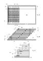
- FIG. 1 is a diagrammatic sketch in a perspective view showing a die mounted onto a support.
- FIG. 2A is a diagrammatic sketch in a plan view showing a die mounted onto a support as in FIG. 1 .
- FIGS. 2B and 2C are diagrammatic sketches in sectional views showing a die mounted onto a support as in FIG. 1 , as indicated at B-B and C-C, respectively.
- FIGS. 3A and 3B are diagrammatic sketches showing an offset die stack mounted on and electrically connected to a support, in plan view ( FIG. 3A ) and in a sectional view ( FIG. 3B ).
- FIG. 3C is a diagrammatic sketch showing a portion of the sectional view of FIG. 3B , enlarged.
- FIG. 4A is a diagrammatic sketch in a partial plan view showing the offset edges of an example of an 8-die offset stack, interconnected.
- FIG. 4B is a diagrammatic sketch in a partial sectional view of an 8-die offset stack, as indicated at B-B in FIG. 4A , interconnected.
- FIG. 5 is a diagrammatic sketch in a sectional view showing an example of a stacked die assembly constructed according to one of the approaches outlined above, having a thicker bottom die.
- FIGS. 6A , 6 B and 6 C are diagrammatic sketches in sectional views showing examples of stacked die assemblies constructed according to another of the approaches outlined above, having a nonfunctional die situated at the substrate.
- FIGS. 7A , 7 B and 7 C are diagrammatic sketches in sectional views showing examples of stacked die assemblies constructed according to another of the approaches outlined above, having zones near the corners of the die left free of electrical connection.
- FIGS. 8A , 8 B and 8 C are diagrammatic sketches in sectional views showing examples of stacked die assemblies constructed according to another of the approaches outlined above, having underfill formed at various locations between the bottom die in the stack and the substrate.
- FIGS. 9A , 9 B and 9 C are diagrammatic sketches in sectional views showing examples of stacked die assemblies constructed according to another of the approaches outlined above, having an underfill fillet formed at the inside corner defined by a die sidewall and an underlying surface.
- FIGS. 10A and 10B are diagrammatic sketches showing an example of a stacked die assembly constructed according to another of the approaches outlined above, having structures limiting the flow of underfill material over the substrate surface.
- FIG. 10B is a partial plan view; and
- FIG. 10A is a sectional view taken at A-A in FIG. 10B .
- FIG. 1 there is shown in a perspective view a semiconductor die 10 mounted over a substrate 110 .
- the die 10 has two larger generally parallel, generally rectangular sides, and four sidewalls. One larger side may be referred to as the front side, and the other may be referred to as the back side.
- the circuitry of the die is situated at or near the die surface at the front side, and so the front side may be referred to as the active side of the die.
- the die 10 is shown with the active side facing away from the substrate 110 , so that the front side 12 of die 10 is visible. Also visible in the view shown in FIG. 1 are sidewalls 14 and 16 of die 10 .
- Margins of the die are adjacent the sidewalls; for example, margin 17 is adjacent the sidewall 14 on the front side 12 of die 10 .
- the intersection of a die sidewall and the front side define a front edge; for example front edge 13 is defined at the intersection of die sidewall 14 and the front side 12 .
- Interconnect pads are arranged in a margin along a front edge; in the example shown here pads 18 are arranged in a row 19 in or near the margin 17 along a front edge 13 of die 10 .
- a die edge along which pads are arranged may be referred to as an “interconnect edge”, and the adjacent margin and die sidewall may be referred to as an “interconnect margin” and an “interconnect sidewall”, respectively.
- the die 10 is mounted onto a die attach side 112 of the substrate 110 by means of a die attach film 15 .
- a number of substrates are formed in one or more rows in a strip and subsequently separated by sawing or punching.
- bond pads 118 are arranged in a row 119 at the die attach side 112 of the substrate 110 , and the die is situated so that the die pads 18 are generally aligned with corresponding bond pads 118 on the substrate.
- Electrical connection (not shown in FIG.
- the die pads 18 with corresponding bond pads 118 is made by applying traces of an electrically conductive material in a flowable form over the respective die pads and bond pads, and then curing the material (or allowing the material to cure) to complete the interconnect.
- the directional axes X and Y parallel to, and Z perpendicular to, the plane of the larger sides of the die (and the plane of the die attach side of the substrate) are indicated at 11 in FIG. 1 and at 21 in FIGS. 2A , 2 B and 2 C.
- the various materials in an assembly such as is illustrated for example in FIG. 1 may have different thermal expansion characteristics (different coefficients of thermal expansion, “CTE”). Particularly, there may be a CTE mismatch between the die (silicon) and the die attach film. Thermal cycling of the construct can cause stresses and strains in the construct, which may result in fatigue-driven degradation of the contact between the interconnect and the die pads or the bond pads, or of the interconnect itself.
- CTE coefficients of thermal expansion
- FIGS. 2A , 2 B and 2 C show a die 20 mounted on a substrate 210 in plan view ( FIG. 2A ) and in sectional views ( FIGS. 2B , 2 C).
- the die 20 is mounted onto a die attach side 212 of the substrate 210 by means of a die attach film 25 .
- die pads 28 , 28 ′ are arranged in rows 29 , 29 ′ along interconnect margins 27 , 27 ′ at opposite front die edges 23 , 23 ′.
- Corresponding bond pads 218 , 218 ′ are arranged in rows 219 , 219 ′ at the die attach side 212 of the substrate, and the die is situated so that the die pads 118 , 118 ′ are generally aligned with corresponding bond pads 218 , 218 ′ on the substrate.
- Electrical connection (not shown in these FIGs.) of the die pads 118 , 118 ′ with corresponding bond pads 218 , 218 ′ is made by applying traces of an electrically conductive material in a flowable form over the respective die pads and bond pads, and then curing the material (or allowing the material to cure) to complete the interconnect.
- the tendencies of the various components to contract or expand in relation to one another is illustrated by the arrows 21 .
- the tendencies of the various components to expand or contract differently can result in relative movement of the parts; for example, the die edges may move in relation to the underlying substrate. More usually, where the various components are securely affixed to one another, the tendencies of the various components to expand or contract differently can result in a curling or warping of the structure or of parts of the structure. This distortion of the shape can cause failure of some interconnections, by causing a crack or break in the interconnect itself, or by partial or complete delamination of the interconnect from one or more pads.
- FIG. 3A shows in a plan view an arrangement of offset stacked die 34 a - 34 h , each die having interconnect pads arranged in one margin adjacent a front die edge; and FIG. 3B shows the stack in a sectional view as indicated at 1 B- 1 B in FIG. 3A .
- interconnect pads 32 are in this example situated in a row 312 alongside a front die edge 311 .
- the die 34 h in this example is covered on all surfaces (back surface 33 , front surface 35 , sidewalls 31 ) by an electrically insulative conformal coating 37 , provided with openings exposing interconnect pads 32 .
- Successive coated die in the stack may, as in these examples, rest directly one upon another, such that the coating on the back side of an upper die can contact the coating on the front side of the underlying die.
- a die attach film may be laminated onto the back side of one or more of the die.
- each die has interconnect pads situated in a margin along one front die edge (an “interconnect” edge), and succeeding die in the stack are arranged so that their respective interconnect edges face toward the same face of the stack. Successive die in the stack are displaced (offset) in a direction orthogonal to the die edge along which the pads are situated, and in the example shown here the offset leaves the pads in each underlying die fully exposed.
- This configuration presents as a stairstep die stack, and electrical interconnections are made over the steps.
- the stack is mounted on a support (for example, a package substrate) having a row 316 of bond sites 36 exposed at a die mount surface 39 .
- the bond sites are connected to (or constitute a part of) electrical circuitry (not shown in the FIGs.) in the support.
- the die stack is affixed to the die mount surface 39 of the substrate, and arranged so that the front sidewall 31 a of a first die 34 a is aligned along the row 316 of bond sites 36 .
- the coated back side of the first die may, as in these examples, directly contact the support surface 39 and may serve to affix the stack to the support.
- a die attach film may be laminated onto the back side of the first die to serve to affix the stack to the support.
- the die are electrically interconnected (die-to-die) in the stack, and the stack is electrically connected to the support, by traces 318 of an interconnect material disposed in contact with die pads and bond pads.
- the interconnect material may be an electrically conductive polymer, such as a polymer matrix containing particles of an electrically conductive material.
- the material may a curable polymer, for example, such as electrically conductive epoxy (for example, a silver filled epoxy); and the interconnection may be made by forming traces of the uncured material in a prescribed pattern and thereafter curing the polymer to secure the electrical contacts with the die pads and the bond sites, and to ensure the mechanical integrity of the traces between them.
- FIG. 3C shows a portion (indicated by the broken outline 3 C in FIG. 3B ) of a stack as in FIGS. 3A and 3B enlarged.
- the die are covered on all surfaces by an electrically insulative conformal coating; that is, for example, the back surface 33 a , the front surface 35 a , and the sidewall 31 a of die 34 a are covered by conformal coating 37 .
- the coating is provided with openings exposing the interconnect pads 32 a .
- the die are offset; that is, for example, the edge 311 b of die 34 b is set back (to the right in the FIG.) in relation to edge 311 a of die 34 a so that pad 32 a on die 34 a is exposed.
- the die stack is situated on the surface 39 of the support such that the edge 31 a of the first (lowest) die 34 a is aligned with the bond pad 36 , and the bond pad is at least partly exposed.
- the electrically conductive interconnect 318 contacts the bond pad 36 , the die pad 32 a , and the die pad 32 b (and successive die pads in the overlying die), and it is disposed upon the coating 37 , which electrically insulates the interconnect from the underlying die surfaces.
- modeling the system in some instances together with observation of failed interconnects reveals cracks or breaks in the interconnects at the “inside corner” where the backside edge (e.g., edge 331 a in FIG. 3C ) of the lowermost die in the stack meets the underlying substrate.
- pads on the die are made available for electrical connection by selectively removing the electrically insulative coating over the pads.
- the interconnect material is deposited over the die in the stack, the material contacts only the exposed pads, and no electrical contact is made with pads (or with other die surfaces overlain by the interconnect material) that remain covered by the electrically insulative coating.
- FIGS. 3A , 3 B, 3 C all the pads on all the die are shown as being exposed for electrical connection by the conductive traces and, accordingly, each of the pads in each die is in these examples electrically connected to pads on the other die in the stack and to a bond pad on the substrate.
- the electrically insulative coating over selected ones of the pads on each die may be removed to expose the selected pads, and the coating may be left in place on pads to which electrical connection is not desired. This may be referred to as a “subtractive procedure” for making pads selectively available for electrical contact. Or, alternatively, in an “additive procedure”, an electrically insulative coating may be applied selectively to areas over which the electrical traces may be formed, at which no electrical contact is intended.
- interconnect failure can result from transverse cracks in the trace itself, which typically propagate from a surface of the trace material, and which may occur during or following molding or encapsulation, such as during thermal testing or during thermal cycling in use.
- the interconnect traces can be coated with a film of a material such as a polymer (for example, a parylene or a silicone rubber) prior to the encapsulating or molding procedure.
- a material such as a polymer (for example, a parylene or a silicone rubber) prior to the encapsulating or molding procedure.
- a silicone rubber such as a room-temperature-vulcanizing silicone elastomer, can be suitable, these are available for example from Dow Corning.
- the film provides a sort of relief or lubrication at the interface of the interconnect material and the molding material or encapsulant, and thereby reduces stresses that may result in crack formation.
- Other materials can be selected to provide such stress relief or lubrication.
- FIGS. 4A , 4 B An assembly made using a subtractive procedure for making pads selectively available for connection is illustrated in FIGS. 4A , 4 B.
- FIG. 4A shows by way of example a portion near the interconnect edge of an 8-die offset stack in a plan view.
- Each die has a row 49 of pads (e.g., pads 48 ; 32 pads in this example).
- the pads may be referenced by numbers 1 through n ( 1 - 32 in this example) according to the pad locations, as suggested by the numerals in parentheses ( 1 ), ( 2 ), ( 3 ) . . . ( 30 ), ( 31 ), ( 32 ) aligned with the pad positions on die 40 .
- the die are stacked one over another and offset so that the interconnect edge of each die (except the lowermost die) is set back with respect to the interconnect edge of the die underlying it.
- the die are arranged in the stack so that corresponding pad locations are aligned in columns.
- the stack is mounted on a support (here a substrate) 400 having interconnect sites (bond pads or leads) 46 .
- the lowermost die in the stack is oriented with the substrate so that the stack edge (that is, the lower die interconnect edge) overlaps the leads on the substrate, and so that the pad columns are aligned with the leads, so in this example there is no interconnect span dimension next to the stack.
- the die stack in this example is covered with a conformal insulative coating 47 (of a material such as for example a parylene). Openings through the conformal coating were made (for example by laser ablation) to expose selected interconnect die pads (pads 48 , for example), while leaving selected other interconnect die pads protected (electrically insulated).
- a conformal insulative coating 47 of a material such as for example a parylene. Openings through the conformal coating were made (for example by laser ablation) to expose selected interconnect die pads (pads 48 , for example), while leaving selected other interconnect die pads protected (electrically insulated).
- FIGS. 4A , 4 B show the interconnect portion of an 8-die offset stack, electrically interconnected with interconnect traces formed over the pad columns (e.g., traces 418 over columns ( 1 ), ( 2 ), ( 3 )).
- FIG. 4B is a sectional view thru the construct of FIG. 4A at the pad location ( 2 ) column, as indicated at B-B in FIG. 4A .
- the pads in the upper four die e.g., pad 48 in the fourth die from the top
- the bond pad 46 on the substrate are exposed by openings in the conformal insulative coating; and the pads in the lower four die (as well as an area of the front side inboard from the pads on the top die, and the outboard area of the substrate) are left covered.
- the exposed pads are available for electrical connection by the interconnect trace formed over them, while the covered pads (and other covered surfaces) are insulated from contact with any overlying electrical traces.
- the traces 418 electrically connect exposed die pads in the column (e.g., pad 48 ) to other exposed die pads in the column and to a corresponding interconnect site 46 on the substrate 400 . Pads that remain covered by the insulative coating and other die surfaces overlain by the interconnect material are not electrically connected.
- the interconnect material is a material that can be applied in a flowable form, and thereafter cured or allowed to cure to form the conductive traces.
- the stack of die may be supported, for example, at the back side of the lowest of the die in the stack, and the interconnect material may be applied along a trajectory over the pads to be connected and the die surfaces between them.
- the interconnect material may be applied using an application tool such as, for example, a syringe or a nozzle. The material exits the tool in a deposition direction generally toward the interconnect terminals, and the tool is moved over the die stack face in a work direction. The material is deposited while the tool is moved.
- the material may be extruded from the tool in a continuous flow, or, the material may exit the tool dropwise.
- the material may exit the tool as a jet of droplets, and is deposited as dots which coalesce upon or following contact with a stack face surface.
- the droplets may be very small, and may exit the tool as an aerosol spray.
- the interconnect material may be an electrically conductive polymer, such as a polymer filled with particles of an electrically conductive material.
- the material may be a curable polymer, for example, such as electrically conductive epoxy (for example, as silver filled epoxy); and, the interconnect process may include forming traces of the uncured material in a prescribed pattern and thereafter curing the polymer to secure the electrical contacts with the terminals and to secure the mechanical integrity of the traces between them.
- the interconnect material may be an electrically conductive ink.
- FIG. 5 illustrates an example of an assembly in which the bottom die 51 in the stack has a greater thickness than the other die 52 , 53 , 54 , 55 , 56 , 57 , 58 in the stack.
- die attach films may be employed, and a conformal dielectric coating (or other electrical insulation) may be provided over surfaces not intended to be electrically connected to overlying electrically conductive traces.
- the interconnect traces are not shown in this drawing.
- the die 52 , 53 , 54 , 55 , 56 , 57 , 58 may have been singulated form a wafer that was thinned (for example in a backgrinding operation) to a desired thinness; and the die 51 may have been singulated from a wafer that was thinned to a greater thickness than the others.
- the bottom die may have the same (or similar) functionality as the other die in the stack; for example all the die in this stack may be memory die. Or, the bottom die may have a functionality different from that of the other die in the stack; for example the thicker bottom die may be a processor die, and the other die may be memory die.
- Other die functionalities are contemplated, according to the desired function of the completed assembly.
- the greater thickness of the bottom die provides increased stiffness to the stack, and can help to reduce warping or bending. What thickness may be required for the bottom die may depend upon, among other factors, the overall dimensions of the package, the thinness of the other die, and the extent of the CTE mismatch in the various components of the assembly.
- FIGS. 6A , 6 B and 6 C illustrate examples of stacked die assemblies in which a nonfunctional die is situated between the lowest functional die in the stack and the substrate.
- the nonfunctional die 60 is a “dummy” die; that is, it has no electronic functionality.
- an 8-die stack of die 51 , 52 , 53 , 54 , 55 , 56 , 57 , 58 is mounted over the dummy die.
- An effect of the dummy die is to raise the horizon of the die pads (that is, the interconnect edge) on the lowest functional die 51 in relation to the bond pads on the substrate 500 .
- the nonfunctional die 62 has electronic circuitry and peripheral die pads and it may be configured substantially the same as the lowest functional die 51 in the stack.
- the die pads on the nonfunctional die 62 are disabled, as symbolized in the drawing by the “X” over the pad.
- the pad may be, for example covered by a dielectric material, so that the additional die is not electrically connected to overlying interconnect traces. Or, for example the electrical connection of the pad to the circuitry on the die may be severed.
- the nonfunctional die is an additional die; that is, the nonfunctional is interposed between the die stack and the substrate.
- the example in FIG. 6C is similar to that in FIG. 6B , except that here the nonfunctional die 61 is the lowermost die of the die stack itself, disabled in a manner for example as described above with reference to FIG. 6B . Because the lowermost die in the stack may have been fully functional before it was disabled, the die 61 may be referred to as a “sacrificial” die.
- FIGS. 7A , 7 B and 7 C illustrate examples of stacked die assemblies in which zones near the corners of the die are left free of electrical connection.
- the “keepout” zones 72 may constitute portions of the interconnect margin of the die at which no pads are situated.
- this arrangement may designed into the placement of pads in a rerouting pattern; or, this arrangement may result during the die singulation process, by cutting the die wider than would be minimally required for the circuitry and the pad arrangement.
- the “keepout” zones 74 constitute disabling interconnection to pads at one or a few die pad positions (“sacrificial pad positions”) near the affected corner; in the illustrated example the die pads in the sacrificial pad positions ( 1 ), ( 2 ), ( 3 ), and ( 30 ), ( 31 ), ( 32 ) are covered by a dielectric material (and no openings are formed over these columns of pads), so that the die is not electrically connected to overlying interconnect traces in the keepout zones.
- the “keepout” zones 76 are established not by disabling pads on the die, but in disabling bond pads at the corresponding positions on the substrate, or by designing the substrate so that no bond pads are located there. In the example illustrated, the bond pads in the keepout zones 76 remain covered by the substrate surface solder mask, or other substrate surface insulation.
- FIGS. 8A , 8 B, 8 C illustrate examples of stacked die assemblies in which an underfill is formed near one or more edges of the bottom die between the bottom die in the stack and the substrate.
- the underfill reinforces the adhesion of the die stack to the substrate, and helps prevent or reduce delamination along the edge.
- An underfill is illustrated for example in FIG. 8A .
- Each of the die 51 , 52 , 53 , 54 , 55 , 56 , 57 , 58 in the stack here is affixed to the underlying die (or to the substrate) by a die attach film; for example, film 518 affixes die 58 to the underlying die 57 , and film 511 affixes die 51 to the substrate 500 .
- Die attach film 511 is dimensioned so that some space between the die and the substrate is left unfilled by the film, adjacent the interconnect die edge.
- a quantity of underfill material is deposited at the die edge, and flows into this space, as shown at 82 in FIG. 8A , and may form a “fillet” 83 at the die sidewall.
- the underfill may be applied in particular spots, at intervals along an edge, as illustrated for example in FIG. 8B , or continuously along an edge.
- an electrically non-conductive underfill material is deposited at spots along the die interconnect sidewall, e.g. spots 83 , generally between the bond pads, e.g., bond pads 85 .
- the underfill once deposited may flow into any space between the bottom die and the substrate.
- an underfill material is deposited at spots, e.g. spots 86 , along the bottom die edge, near the corners of the bottom die.
- spots e.g. spots 86
- the underfill once deposited may flow into any space between the bottom die and the substrate.
- an underfill is deposited in a continuous line along one or more of the non-interconnect sidewalls.
- an electrically conductive underfill it can be deposited at any location where the underfill will not cause electrical shorting.
- the underfill approach can be employed for die stacks in which the die are offset, as illustrated here; or for die stacks where each die in the stack is smaller in at least one dimension that the die beneath (pyramid stack), or in stacks where successive die in the stack are staggered and may be rotated. Such configurations are described, for example, in U.S. application Ser. No. 12/124,077, referenced above.
- Electrically conductive or electrically nonconductive underfill materials may be used. Where an electrically conductive underfill is used, it can be deposited at any location where the underfill will not cause electrical shorting.
- the underfill material may be applied using standard equipment, and may be applied either prior to or subsequent to formation of the electrical interconnect traces.
- FIGS. 9A , 9 B and 9 C illustrate examples of stacked die assemblies in which an underfill material is deposited to form a fillet at the inside angle formed by a die sidewall and an underlying surface.
- FIG. 9A illustrates a configuration in which the die sidewall is the interconnect sidewall 94 of an upper die 93 , and the underlying surface is an electrically insulated area 96 of the front side of an underlying die 52 , inboard of the die pads on the underlying die and adjacent the upper die sidewall.
- the deposited underfill material forms a fillet 90 which provides a gradually sloping surface extending from the upper die interconnect edge to the underlying die surface inboard from the die pads, on which an electrical interconnect trace 91 can be formed, electrically connecting the pads on the upper die 53 and the underlying die 52 (and connecting additional die, e.g., die 51 as appropriate) to circuitry in the substrate 500 .
- a standard underfill material can be used, and it can be deposited using standard equipment for applying underfill.
- Preferred underfill material may be high modulus materials, having good CTE matching with other materials in the assembly.
- one suitable standard underfill material is marketed under the name Namics U8439-1.
- FIG. 9B shows a configuration in which die 51 and 52 are mounted die-up over a flip-chip die 91 mounted die-down on the substrate 500 , and in which an underfill fillet 900 is formed at the inside angle formed by sidewalls 914 , 924 of the die 51 and the flip chip die 91 , and the surface 916 of the underlying substrate 500 inboard from the bond pads.
- an additional fillet 902 is formed at the inside angles formed by the interconnect sidewall of the die 52 and the surface of the underlying die 51 inboard from the bond pads.
- the fillets 900 , 902 provide a gradually sloping surface extending from the upper die 52 interconnect edge to the underlying die surface inboard from the die pads, and then from the die 51 interconnect edge to the underlying substrate surface inboard from the bond pads, on which an electrical interconnect trace 911 can be formed, electrically connecting the pads on the upper die 52 and the underlying die 51 to circuitry in the substrate 500 .
- FIG. 9C shows a further example, in which an underfill fillet 932 is formed at the inside angle formed between an interconnect sidewall of a die 53 and a surface of an underlying die 52 ; and an underfill fillet 934 is formed at the inside angle formed between an interconnect sidewall of a bottom die 51 and a surface of the underlying substrate 500 ; and an interconnect trace 931 is deposited on the fillet 934 to connect the bottom die 51 to a first row of bond pads on the substrate 550 ; and thereafter an underfill fillet 936 is formed over the fillet 934 and the trace 931 ,; and thereafter an interconnect trace 941 is formed over the fillet 932 and the fillet 936 to connect the upper die 53 to the die 52 and to a second, outboard, row of bond pads on the substrate 500 .
- the underfill may be formed so that it forms a fillet approximating a right triangular shape in transverse section; viewed in this way the hypotenuse of the triangle shape is a sloping surface over which an interconnect trace can be formed; and a vertical side of the triangle forms an angle with the hypotenuse at or near the upper die interconnect edge.
- the sloping surface of the fillet may be slightly concave or convex, or may be a more complex slightly curved surface.
- the underfill can be CTE matched, to help stabilize the assembly, reducing delamination effects.
- the underfill shaped as described above, can provide a gradual transition from die-to-die or from die-to-substrate, eliminating abrupt angular (approximately right-angle) transitions at the interconnect edges of the die and at the inside corners where the back edge of the die sidewall meets the underlying surface.
- a first underfill fillet formed at the sidewall of a bottom die and a substrate can support a first set of electrical interconnect traces connecting pads on the bottom die with bond pads in a first row on the substrate; and an additional underfill fillet formed over the first interconnect traces on the first fillet at the sidewall of an upper die and the bottom die can support a second set of interconnect traces from die pads on the upper die to bond pads in a second row, outboard from the first row, on the substrate.
- FIGS. 10A and 10B illustrate examples of approaches to assist in constraining the flow (“run-out” or “bleed”) of the underfill material over the substrate.
- FIG. 10A is presented in a partial sectional view similar to that of FIG. 9B , in part; and FIG. 10B is presented in a partial plan view, in which the sectional view of FIG. 10A is indicated by the arrow A-A.
- FIG. 10 show a configuration in which a die 51 is mounted die-up over a flip-chip die 91 mounted die-down on a die attach side of the substrate 1000 , and in which an underfill fillet 1900 is formed at the inside angle formed by sidewalls 914 , 924 of the die 51 and the flip chip die 91 , and the surface 1916 of the underlying substrate 1000 inboard from the bond pads 1020 .
- the fillets 1900 provides a gradually sloping surface extending from an upper die (out of the frame of the drawing) to the underlying surface of die 51 inboard from the die pads 5120 , and then from the die 51 interconnect edge to the underlying substrate surface inboard from the bond pads 1020 , on which an electrical interconnect trace 1021 can be formed, electrically connecting the pads on the upper die and the die 51 to circuitry in the substrate 1020 .
- the die attach side of the substrate 1000 is covered by a solder mask 1010 , and a trench having trench walls 1013 through the solder mask 1010 exposes bond pads 1020 on the substrate 1000 for connection.
- FIGs. illustrate an example of an approach for limiting the bleed or run-out of the underfill material over the substrate surface, in which the die attach side of the substrate 1000 is covered by a solder mask 1010 .
- the trench in the solder mask has trench walls 1013 , 1013 ′, and at least trench wall 1013 , nearer the die, is situated generally parallel to the row of bond pads on the substrate (and generally parallel to the interconnect sidewall of the die).
- the advancing front of the flowing material halts substantially at the edge of the trench wall 1013 , as indicated at 1023 . That is, the trench wall 1013 prevent run-out or bleed of the underfill material over the bond pads 1020 that are exposed within the trench.
- FIG. 10B additionally illustrates an example of an additional approach to limiting the bleed or run-out of the underfill material over the substrate surface.
- This approach may be used whether or not the substrate has a solder mask, and may be used either without the trench approach or in addition to it.
- a dam 1030 , 1030 ′ is provided at the location of each side of the underfill fillet prior to depositing the underfill material, to limit or prevent flow of the underfill material laterally, that is, in directions generally parallel to the row of die pads.
- the dam material may be a curable material applicable in a flowable form and thereafter cured or allowed to cure, and the dam material may have properties that make it generally less likely than the underfill material to flow (run-out or bleed) when in an uncured state.
- the dam material may have a higher viscosity, for example, than the underfill material.
- the dam material and the underfill material may be cured in the same cure procedure, or the dam material may be cured in an earlier cure procedure.
- the underfill can be one marketed by Namics Corporation under the name “Chipcoat”, such as the “Chipcoat U8439-1”.
- a suitable dam material can be one marketed by Lord Thermoset under the name “CircuitSAFTM”, such as the “CircuitSAFTM ME-456”.
- This dam material applied prior to depositing the underflow material, prevents or limits lateral flow of this underfill material; and both materials can be cured in one cure procedure, which may be for example heating the assembly at 165° C. for about 1 hour.
- Other suitable materials may be selected without undue experimentation.
Abstract
Description
Claims (24)
Priority Applications (1)
| Application Number | Priority Date | Filing Date | Title |
|---|---|---|---|
| US12/939,524 US8912661B2 (en) | 2009-11-04 | 2010-11-04 | Stacked die assembly having reduced stress electrical interconnects |
Applications Claiming Priority (2)
| Application Number | Priority Date | Filing Date | Title |
|---|---|---|---|
| US28058409P | 2009-11-04 | 2009-11-04 | |
| US12/939,524 US8912661B2 (en) | 2009-11-04 | 2010-11-04 | Stacked die assembly having reduced stress electrical interconnects |
Publications (2)
| Publication Number | Publication Date |
|---|---|
| US20110272825A1 US20110272825A1 (en) | 2011-11-10 |
| US8912661B2 true US8912661B2 (en) | 2014-12-16 |
Family
ID=43970756
Family Applications (1)
| Application Number | Title | Priority Date | Filing Date |
|---|---|---|---|
| US12/939,524 Active US8912661B2 (en) | 2009-11-04 | 2010-11-04 | Stacked die assembly having reduced stress electrical interconnects |
Country Status (3)
| Country | Link |
|---|---|
| US (1) | US8912661B2 (en) |
| TW (1) | TWI544604B (en) |
| WO (1) | WO2011056987A2 (en) |
Cited By (2)
| Publication number | Priority date | Publication date | Assignee | Title |
|---|---|---|---|---|
| US20150031170A1 (en) * | 2012-07-06 | 2015-01-29 | Samsung Electronics Co., Ltd. | Method and apparatus for stacked semiconductor chips |
| US20210272934A1 (en) * | 2019-08-10 | 2021-09-02 | Amkor Technology Singapore Holding Pte. Ltd. | Semiconductor devices and methods of manufacturing semiconductor devices |
Families Citing this family (15)
| Publication number | Priority date | Publication date | Assignee | Title |
|---|---|---|---|---|
| US8829677B2 (en) | 2010-10-14 | 2014-09-09 | Invensas Corporation | Semiconductor die having fine pitch electrical interconnects |
| US8587088B2 (en) | 2011-02-17 | 2013-11-19 | Apple Inc. | Side-mounted controller and methods for making the same |
| KR20120135626A (en) * | 2011-06-07 | 2012-12-17 | 삼성전자주식회사 | Method for manufacturing semiconductor chip package |
| US20130075892A1 (en) * | 2011-09-27 | 2013-03-28 | Taiwan Semiconductor Manufacturing Company, Ltd. | Method for Three Dimensional Integrated Circuit Fabrication |
| US9196588B2 (en) * | 2011-11-04 | 2015-11-24 | Invensas Corporation | EMI shield |
| US8847412B2 (en) | 2012-11-09 | 2014-09-30 | Invensas Corporation | Microelectronic assembly with thermally and electrically conductive underfill |
| CN103474421B (en) * | 2013-08-30 | 2016-10-12 | 晟碟信息科技(上海)有限公司 | High-yield semiconductor device |
| TWI467711B (en) * | 2013-09-10 | 2015-01-01 | Chipbond Technology Corp | Semiconductorstructure |
| KR102107961B1 (en) | 2013-11-14 | 2020-05-28 | 삼성전자 주식회사 | Semiconductor device and method for fabricating the same |
| KR102389816B1 (en) * | 2015-08-25 | 2022-04-22 | 삼성전자주식회사 | Semiconductor device and method of forming patterns for semiconductor device |
| US10790172B2 (en) * | 2018-08-17 | 2020-09-29 | Jabil Inc. | Apparatus, system, and method of providing a ramped interconnect for semiconductor fabrication |
| US10797035B1 (en) * | 2019-04-02 | 2020-10-06 | Sandisk Technologies Llc | Bonded assembly containing side bonding structures and methods of manufacturing the same |
| US11373956B2 (en) * | 2020-01-14 | 2022-06-28 | Advanced Semiconductor Engineering, Inc. | Semiconductor device package and method of manufacturing the same |
| US11456272B2 (en) * | 2020-09-11 | 2022-09-27 | Western Digital Technologies, Inc. | Straight wirebonding of silicon dies |
| WO2022094467A1 (en) * | 2020-11-02 | 2022-05-05 | Samtec, Inc. | Flex circuit and electrical communication assemblies related to same |
Citations (203)
| Publication number | Priority date | Publication date | Assignee | Title |
|---|---|---|---|---|
| US4323914A (en) | 1979-02-01 | 1982-04-06 | International Business Machines Corporation | Heat transfer structure for integrated circuit package |
| US4336551A (en) | 1977-05-30 | 1982-06-22 | Hitachi, Ltd. | Thick-film printed circuit board and method for producing the same |
| US4363076A (en) | 1980-12-29 | 1982-12-07 | Honeywell Information Systems Inc. | Integrated circuit package |
| US4500905A (en) | 1981-09-30 | 1985-02-19 | Tokyo Shibaura Denki Kabushiki Kaisha | Stacked semiconductor device with sloping sides |
| US4784972A (en) | 1984-08-18 | 1988-11-15 | Matsushita Electric Industrial Co. Ltd. | Method of joining beam leads with projections to device electrodes |
| US5107325A (en) | 1989-04-17 | 1992-04-21 | Seiko Epson Corporation | Structure and method of packaging a semiconductor device |
| US5138438A (en) | 1987-06-24 | 1992-08-11 | Akita Electronics Co. Ltd. | Lead connections means for stacked tab packaged IC chips |
| US5200362A (en) | 1989-09-06 | 1993-04-06 | Motorola, Inc. | Method of attaching conductive traces to an encapsulated semiconductor die using a removable transfer film |
| US5218234A (en) * | 1991-12-23 | 1993-06-08 | Motorola, Inc. | Semiconductor device with controlled spread polymeric underfill |
| US5311401A (en) | 1991-07-09 | 1994-05-10 | Hughes Aircraft Company | Stacked chip assembly and manufacturing method therefor |
| US5331591A (en) | 1993-02-01 | 1994-07-19 | At&T Bell Laboratories | Electronic module including a programmable memory |
| US5334872A (en) | 1990-01-29 | 1994-08-02 | Mitsubishi Denki Kabushiki Kaisha | Encapsulated semiconductor device having a hanging heat spreading plate electrically insulated from the die pad |
| FR2704690A1 (en) | 1993-04-27 | 1994-11-04 | Thomson Csf | Method for encapsulating semiconductor wafers, device obtained by this process and application to the interconnection of wafers in three dimensions. |
| US5434745A (en) | 1994-07-26 | 1995-07-18 | White Microelectronics Div. Of Bowmar Instrument Corp. | Stacked silicon die carrier assembly |
| US5466634A (en) | 1994-12-20 | 1995-11-14 | International Business Machines Corporation | Electronic modules with interconnected surface metallization layers and fabrication methods therefore |
| US5538758A (en) | 1995-10-27 | 1996-07-23 | Specialty Coating Systems, Inc. | Method and apparatus for the deposition of parylene AF4 onto semiconductor wafers |
| US5571754A (en) | 1995-07-26 | 1996-11-05 | International Business Machines Corporation | Method of fabrication of endcap chip with conductive, monolithic L-connect for multichip stack |
| US5616953A (en) | 1994-09-01 | 1997-04-01 | Micron Technology, Inc. | Lead frame surface finish enhancement |
| US5629566A (en) | 1994-08-15 | 1997-05-13 | Kabushiki Kaisha Toshiba | Flip-chip semiconductor devices having two encapsulants |
| US5691248A (en) | 1995-07-26 | 1997-11-25 | International Business Machines Corporation | Methods for precise definition of integrated circuit chip edges |
| US5698895A (en) | 1994-06-23 | 1997-12-16 | Cubic Memory, Inc. | Silicon segment programming method and apparatus |
| US5721151A (en) | 1995-06-07 | 1998-02-24 | Lsi Logic Corporation | Method of fabricating a gate array integrated circuit including interconnectable macro-arrays |
| US5731631A (en) | 1996-02-01 | 1998-03-24 | Mitsubishi Denki Kabushiki Kaisha | Semiconductor device with tape automated bonding element |
| US5737191A (en) | 1995-04-07 | 1998-04-07 | Shinko Electric Industries Co., Ltd. | Structure and process for mounting semiconductor chip |
| US5870351A (en) | 1994-10-21 | 1999-02-09 | The Board Of Trustees Of The Leland Stanford Junior University | Broadband microfabriated ultrasonic transducer and method of fabrication |
| WO1999007015A1 (en) | 1997-07-29 | 1999-02-11 | Cubic Memory, Inc. | Conductive epoxy flip-chip on chip |
| WO1999009599A2 (en) | 1997-08-21 | 1999-02-25 | Cubic Memory, Inc. | Vertical interconnect process for silicon segments with dielectric isolation |
| US5879965A (en) | 1997-06-19 | 1999-03-09 | Micron Technology, Inc. | Plastic lead frames for semiconductor devices, packages including same, and methods of fabrication |
| US5891761A (en) | 1994-06-23 | 1999-04-06 | Cubic Memory, Inc. | Method for forming vertical interconnect process for silicon segments with thermally conductive epoxy preform |
| US5910687A (en) | 1997-01-24 | 1999-06-08 | Chipscale, Inc. | Wafer fabrication of die-bottom contacts for electronic devices |
| US5946545A (en) | 1994-03-30 | 1999-08-31 | Internatinal Business Machines Corporation | Semiconductor stack structures and fabrication/sparing methods utilizing programmable spare circuit |
| JPH11260851A (en) | 1998-03-11 | 1999-09-24 | Matsushita Electric Ind Co Ltd | Semiconductor device and its manufacture |
| US5965947A (en) | 1996-08-20 | 1999-10-12 | Samsung Electronics Co., Ltd. | Structure of a semiconductor package including chips bonded to die bonding pad with conductive adhesive and chips bonded with non-conductive adhesive containing insulating beads |
| US6030854A (en) | 1996-03-29 | 2000-02-29 | Intel Corporation | Method for producing a multilayer interconnection structure |
| US6034438A (en) | 1996-10-18 | 2000-03-07 | The Regents Of The University Of California | L-connect routing of die surface pads to the die edge for stacking in a 3D array |
| US6087716A (en) | 1997-02-03 | 2000-07-11 | Nec Corporation | Semiconductor device package having a connection substrate with turned back leads and method thereof |
| US6107164A (en) | 1998-08-18 | 2000-08-22 | Oki Electric Industry Co., Ltd. | Using grooves as alignment marks when dicing an encapsulated semiconductor wafer |
| JP2000269411A (en) | 1999-03-17 | 2000-09-29 | Shinko Electric Ind Co Ltd | Semiconductor device and manufacture thereof |
| EP1041624A1 (en) | 1999-04-02 | 2000-10-04 | Interuniversitair Microelektronica Centrum Vzw | Method of transferring ultra-thin substrates and application of the method to the manufacture of a multilayer thin film device |
| US6175158B1 (en) | 1998-09-08 | 2001-01-16 | Lucent Technologies Inc. | Interposer for recessed flip-chip package |
| US6228686B1 (en) | 1995-09-18 | 2001-05-08 | Tessera, Inc. | Method of fabricating a microelectronic assembly using sheets with gaps to define lead regions |
| US6255726B1 (en) | 1994-06-23 | 2001-07-03 | Cubic Memory, Inc. | Vertical interconnect process for silicon segments with dielectric isolation |
| KR20010062722A (en) | 1999-12-28 | 2001-07-07 | 루이스 에이. 헥트 | System for testing bare ic chips and a socket for such chips |
| US6262476B1 (en) | 1998-07-27 | 2001-07-17 | Siemens Aktiengesellschaft | Composite member composed of at least two integrated circuits and method for the manufacture of a composite member composed of at least two integrated circuits |
| JP2001210782A (en) | 2000-01-27 | 2001-08-03 | Seiko Epson Corp | Semiconductor chip, multi-chip package, semiconductor device, and electronic equipment using it |
| WO2001064344A2 (en) | 2000-03-02 | 2001-09-07 | Microchips, Inc. | Microfabricated devices for the storage and selective exposure of chemicals and devices |
| US6297657B1 (en) | 1999-01-11 | 2001-10-02 | Wentworth Laboratories, Inc. | Temperature compensated vertical pin probing device |
| US6303977B1 (en) | 1998-12-03 | 2001-10-16 | Texas Instruments Incorporated | Fully hermetic semiconductor chip, including sealed edge sides |
| US20010031548A1 (en) | 1997-10-20 | 2001-10-18 | Peter Elenius | Method for forming chip scale package |
| US6315856B1 (en) | 1998-03-19 | 2001-11-13 | Kabushiki Kaisha Toshiba | Method of mounting electronic component |
| US6326689B1 (en) | 1999-07-26 | 2001-12-04 | Stmicroelectronics, Inc. | Backside contact for touchchip |
| US6326244B1 (en) | 1998-09-03 | 2001-12-04 | Micron Technology, Inc. | Method of making a cavity ball grid array apparatus |
| US6338980B1 (en) | 1999-08-13 | 2002-01-15 | Citizen Watch Co., Ltd. | Method for manufacturing chip-scale package and manufacturing IC chip |
| US20020006686A1 (en) | 2000-07-12 | 2002-01-17 | Cloud Eugene H. | Die to die connection method and assemblies and packages including dice so connected |
| US6351030B2 (en) | 1997-09-29 | 2002-02-26 | International Business Machines Corporation | Electronic package utilizing protective coating |
| US20020027257A1 (en) | 2000-06-02 | 2002-03-07 | Kinsman Larry D. | Method for fabricating a chip scale package using wafer level processing and devices resulting therefrom |
| US20020045290A1 (en) | 1996-02-20 | 2002-04-18 | Michael B. Ball | Flip chip and conventional stack |
| US20020096349A1 (en) | 2001-01-24 | 2002-07-25 | Harry Hedler | Electronic component with a semiconductor chip and method of producing the electronic component |
| US20020127775A1 (en) | 1999-12-23 | 2002-09-12 | Rambus Inc. | Redistributed bond pads in stacked integrated circuit die package |
| US6472746B2 (en) * | 2000-08-02 | 2002-10-29 | Fujitsu Limited | Semiconductor device having bonding wires serving as external connection terminals |
| US6476467B2 (en) * | 1997-01-31 | 2002-11-05 | Hitachi, Ltd. | Semiconductor device and process for producing the same |
| US20020168798A1 (en) | 1996-10-31 | 2002-11-14 | Glenn Thomas P. | Method of making near chip size integrated circuit package |
| US20020180010A1 (en) | 1996-11-21 | 2002-12-05 | Kunihiro Tsubosaki | Semiconductor device and manufacturing method thereof |
| US20020187260A1 (en) | 2001-05-30 | 2002-12-12 | Sheppard Norman F. | Conformal coated microchip reservoir devices |
| US20020185725A1 (en) | 1998-08-21 | 2002-12-12 | Moden Walter L. | Low profile multi-IC chip package connector |
| US20030038357A1 (en) | 2001-08-24 | 2003-02-27 | Derderian James M. | Spacer for semiconductor devices, semiconductor devices and assemblies including the spacer, and methods |
| US20030038356A1 (en) | 2001-08-24 | 2003-02-27 | Derderian James M | Semiconductor devices including stacking spacers thereon, assemblies including the semiconductor devices, and methods |
| US20030038353A1 (en) | 2001-08-23 | 2003-02-27 | Derderian James M. | Assemblies including stacked semiconductor devices separated by discrete conductive elements therebetween, packages including the assemblies, and methods |
| US20030071338A1 (en) | 2001-10-16 | 2003-04-17 | Jeung Boon Suan | Apparatus and method for leadless packaging of semiconductor devices |
| US20030092326A1 (en) * | 2000-06-16 | 2003-05-15 | Hidenobu Nishikawa | Electronic parts packaging method and electronic parts package |
| JP2003142518A (en) | 2001-11-02 | 2003-05-16 | Nec Electronics Corp | Device and method for manufacturing semiconductor, semiconductor device, and electronic device |
| US20030096454A1 (en) | 2001-11-16 | 2003-05-22 | Poo Chia Yong | Stackable semiconductor package and wafer level fabrication method |
| US6569709B2 (en) | 2001-10-15 | 2003-05-27 | Micron Technology, Inc. | Assemblies including stacked semiconductor devices separated a distance defined by adhesive material interposed therebetween, packages including the assemblies, and methods |
| US20030099085A1 (en) | 2001-11-26 | 2003-05-29 | Delaware Capital Formation, Inc. | Surface flashover resistant capacitors and method for producing same |
| JP2003163324A (en) | 2001-11-27 | 2003-06-06 | Nec Corp | Unit semiconductor device and manufacturing method thereof, and three-dimensional laminated semiconductor device |
| USD475981S1 (en) | 2002-03-29 | 2003-06-17 | Mitsubishi Denki Kabushiki Kaisha | Integrated circuits substrate |
| US6580165B1 (en) | 2000-11-16 | 2003-06-17 | Fairchild Semiconductor Corporation | Flip chip with solder pre-plated leadframe including locating holes |
| US20030122243A1 (en) | 2001-12-31 | 2003-07-03 | Jin-Yuan Lee | Integrated chip package structure using organic substrate and method of manufacturing the same |
| US6593648B2 (en) | 2000-08-31 | 2003-07-15 | Seiko Epson Corporation | Semiconductor device and method of making the same, circuit board and electronic equipment |
| US6607938B2 (en) | 2001-07-19 | 2003-08-19 | Samsung Electronics Co., Ltd. | Wafer level stack chip package and method for manufacturing same |
| US6607941B2 (en) | 2002-01-11 | 2003-08-19 | National Semiconductor Corporation | Process and structure improvements to shellcase style packaging technology |
| US6621172B2 (en) | 1999-09-03 | 2003-09-16 | Seiko Epson Corporation | Semiconductor device and method of fabricating the same, circuit board, and electronic equipment |
| US6621155B1 (en) | 1999-12-23 | 2003-09-16 | Rambus Inc. | Integrated circuit device having stacked dies and impedance balanced transmission lines |
| US20030209772A1 (en) | 2002-05-13 | 2003-11-13 | National Semiconductor Corporation | Electrical die contact structure and fabrication method |
| US6656827B1 (en) | 2002-10-17 | 2003-12-02 | Taiwan Semiconductor Manufacturing Co., Ltd. | Electrical performance enhanced wafer level chip scale package with ground |
| US6667543B1 (en) | 2002-10-29 | 2003-12-23 | Motorola, Inc. | Optical sensor package |
| US6670701B2 (en) | 2001-02-01 | 2003-12-30 | Mitsubishi Denki Kabushiki Kaisha | Semiconductor module and electronic component |
| US6674159B1 (en) | 2000-05-16 | 2004-01-06 | Sandia National Laboratories | Bi-level microelectronic device package with an integral window |
| US6706971B2 (en) | 2001-01-26 | 2004-03-16 | Irvine Sensors Corporation | Stackable microcircuit layer formed from a plastic encapsulated microcircuit |
| JP2004119473A (en) | 2002-09-24 | 2004-04-15 | Seiko Epson Corp | Semiconductor device, its manufacturing method, circuit board, and electronic apparatus |
| US6722213B2 (en) | 2000-02-06 | 2004-04-20 | Minitubes Gmbh | Temperature-adjusted sampler for fluids |
| US6737743B2 (en) | 2001-07-10 | 2004-05-18 | Kabushiki Kaisha Toshiba | Memory chip and semiconductor device using the memory chip and manufacturing method of those |
| JP2004153130A (en) | 2002-10-31 | 2004-05-27 | Olympus Corp | Semiconductor device and its manufacturing method |
| JP2004158536A (en) | 2002-11-05 | 2004-06-03 | Fujitsu Ltd | Semiconductor device and method for manufacturing the same |
| US6750547B2 (en) | 2001-12-26 | 2004-06-15 | Micron Technology, Inc. | Multi-substrate microelectronic packages and methods for manufacture |
| US20040113283A1 (en) | 2002-03-06 | 2004-06-17 | Farnworth Warren M. | Method for fabricating encapsulated semiconductor components by etching |
| US6756252B2 (en) * | 2002-07-17 | 2004-06-29 | Texas Instrument Incorporated | Multilayer laser trim interconnect method |
| JP2004214548A (en) | 2003-01-08 | 2004-07-29 | Mitsubishi Electric Corp | Component-built-in board type module, manufacturing method thereof, board having same, and manufacturing method thereof |
| US20040150095A1 (en) | 2003-01-30 | 2004-08-05 | Endicott Interconnect Technologies, Inc. | Stacked chip electronic package having laminate carrier and method of making same |
| CN1531069A (en) | 2003-03-13 | 2004-09-22 | ������������ʽ���� | Electronic device and producing method thereof |
| US20040198033A1 (en) | 2002-08-20 | 2004-10-07 | Lee Teck Kheng | Double bumping of flexible substrate for first and second level interconnects |
| US20040195667A1 (en) | 2003-04-04 | 2004-10-07 | Chippac, Inc | Semiconductor multipackage module including processor and memory package assemblies |
| US6802446B2 (en) | 2002-02-01 | 2004-10-12 | Delphi Technologies, Inc. | Conductive adhesive material with metallurgically-bonded conductive particles |
| US20040212083A1 (en) | 2000-09-21 | 2004-10-28 | Jicheng Yang | Method to prevent die attach adhesive contamination in stacked chips |
| US20040217446A1 (en) | 2003-01-02 | 2004-11-04 | Headley William R. | Method and apparatus for preparing a plurality of dice in wafers |
| US20040238933A1 (en) | 2003-05-27 | 2004-12-02 | Shou-Lung Chen | Stacked package for electronic elements and packaging method thereof |
| US20040251520A1 (en) | 2003-06-10 | 2004-12-16 | Sanyo Electric Co., Ltd. | Method for manufacturing semiconductor device |
| US20040262035A1 (en) * | 2003-06-30 | 2004-12-30 | Bing-Hong Ko | Electronic component mounting structure |
| JP2005005529A (en) | 2003-06-12 | 2005-01-06 | Toshiba Corp | Three dimensionally packaging semiconductor module and three dimensionally packaging semiconductor system |
| US6844623B1 (en) | 2000-05-16 | 2005-01-18 | Sandia Corporation | Temporary coatings for protection of microelectronic devices during packaging |
| US20050013927A1 (en) | 2003-02-06 | 2005-01-20 | Semiconductor Energy Laboratory Co., Ltd. | Manufacturing method for display device |
| KR20050009036A (en) | 2003-07-15 | 2005-01-24 | 삼성전자주식회사 | Stack package and manufacturing method thereof |
| US6849802B2 (en) | 2002-02-06 | 2005-02-01 | Samsung Electronics Co., Ltd | Semiconductor chip, chip stack package and manufacturing method |
| US20050067694A1 (en) | 2003-09-30 | 2005-03-31 | Pon Florence R. | Spacerless die stacking |
| US20050067680A1 (en) | 2003-09-30 | 2005-03-31 | Boon Suan Jeung | Castellated chip-scale packages and methods for fabricating the same |
| US20050085050A1 (en) | 2003-10-21 | 2005-04-21 | Draney Nathan R. | Substrate thinning including planarization |
| US20050082651A1 (en) | 2003-10-20 | 2005-04-21 | Farnworth Warren M. | Methods of coating and singulating wafers and chip-scale packages formed therefrom |
| US20050101039A1 (en) | 2002-10-30 | 2005-05-12 | John Chen | Apparatus and method for stacking laser bars for uniform facet coating |
| US20050104179A1 (en) | 2003-07-03 | 2005-05-19 | Shellcase Ltd. | Methods and apparatus for packaging integrated circuit devices |
| US6910268B2 (en) | 2001-03-27 | 2005-06-28 | Formfactor, Inc. | Method for fabricating an IC interconnect system including an in-street integrated circuit wafer via |
| DE102004039906A1 (en) | 2004-08-18 | 2005-08-18 | Infineon Technologies Ag | Electronic component with a number of integrated members, is formed by producing members with a surface that contains a circuit, and connecting components using bond wires |
| US6940022B1 (en) | 1997-12-18 | 2005-09-06 | Vlt, Inc. | Protective coating for an electronic device |
| US6956283B1 (en) | 2000-05-16 | 2005-10-18 | Peterson Kenneth A | Encapsulants for protecting MEMS devices during post-packaging release etch |
| US20050230802A1 (en) * | 2004-04-13 | 2005-10-20 | Al Vindasius | Stacked die BGA or LGA component assembly |
| US20050248021A1 (en) | 2004-05-06 | 2005-11-10 | Henrik Morkner | Multi-mode integrated circuit structure |
| US20050258530A1 (en) | 2004-04-13 | 2005-11-24 | Al Vindasius | Micropede stacked die component assembly |
| US6972480B2 (en) | 2003-06-16 | 2005-12-06 | Shellcase Ltd. | Methods and apparatus for packaging integrated circuit devices |
| US20050287705A1 (en) | 2004-06-25 | 2005-12-29 | Advanced Semiconductor Engineering, Inc. | Flip chip on leadframe package and method for manufacturing the same |
| US20060003552A1 (en) | 2004-07-01 | 2006-01-05 | Disco Corporation | Wafer dividing method |
| US6984885B1 (en) | 2000-02-10 | 2006-01-10 | Renesas Technology Corp. | Semiconductor device having densely stacked semiconductor chips |
| US20060055050A1 (en) | 2004-09-10 | 2006-03-16 | Hideo Numata | Semiconductor device and manufacturing method thereof |
| US20060068567A1 (en) | 2004-09-24 | 2006-03-30 | Eric Beyne | Method for chip singulation |
| US20060076690A1 (en) | 2004-09-27 | 2006-04-13 | Formfactor, Inc. | Stacked Die Module |
| US20060094165A1 (en) | 2004-10-29 | 2006-05-04 | Harry Hedler | Method for fabricating semiconductor components |
| US20060097356A1 (en) | 2004-11-11 | 2006-05-11 | Fujitsu Limited | Semiconductor substrate, manufacturing method of a semiconductor device and testing method of a semiconductor device |
| US20060103000A1 (en) * | 2004-11-16 | 2006-05-18 | Seiko Epson Corporation | Electronic device package and electronic equipment |
| US20060121645A1 (en) | 1996-05-20 | 2006-06-08 | Ball Michael B | Method of fabrication of stacked semiconductor devices |
| US7061125B2 (en) | 2003-02-07 | 2006-06-13 | Samsung Electronics, Co. Ltd. | Semiconductor package with pattern leads and method for manufacturing the same |
| US20060138626A1 (en) | 2004-12-29 | 2006-06-29 | Tessera, Inc. | Microelectronic packages using a ceramic substrate having a window and a conductive surface region |
| US7115986B2 (en) | 2001-05-02 | 2006-10-03 | Micron Technology, Inc. | Flexible ball grid array chip scale packages |
| US20060220262A1 (en) | 2005-04-04 | 2006-10-05 | Torsten Meyer | Stacked die package |
| US20060267173A1 (en) | 2005-05-26 | 2006-11-30 | Sandisk Corporation | Integrated circuit package having stacked integrated circuits and method therefor |
| US20060273365A1 (en) | 2002-11-21 | 2006-12-07 | Fujitsu Limited | Semiconductor device and its manufacture method, and measurement fixture for the semiconductor device |
| US20060278971A1 (en) | 2005-06-10 | 2006-12-14 | Honeywell International Inc. | Method and apparatus for applying external coating to grid array packages for increased reliability and performance |
| JP2006351793A (en) | 2005-06-15 | 2006-12-28 | Fujitsu Ltd | Semiconductor device |
| KR20070018057A (en) | 2004-03-23 | 2007-02-13 | 텍사스 인스트루먼츠 인코포레이티드 | Vertically stacked semiconductor device |
| US7190060B1 (en) | 2002-01-09 | 2007-03-13 | Bridge Semiconductor Corporation | Three-dimensional stacked semiconductor package device with bent and flat leads and method of making same |
| US20070065987A1 (en) | 2001-06-21 | 2007-03-22 | Mess Leonard E | Stacked mass storage flash memory package |
| JP2007073803A (en) | 2005-09-08 | 2007-03-22 | Toshiba Corp | Semiconductor device and its manufacturing method |
| US7196262B2 (en) | 2005-06-20 | 2007-03-27 | Solyndra, Inc. | Bifacial elongated solar cell devices |
| US7208345B2 (en) | 2005-05-11 | 2007-04-24 | Infineon Technologies Ag | Method of manufacturing a semiconductor device comprising stacked chips and a corresponding semiconductor device |
| US20070102801A1 (en) | 2005-11-10 | 2007-05-10 | Kabushiki Kaisha Toshiba | Stack-type semiconductor device and method of manufacturing the same |
| US7221051B2 (en) | 2004-01-23 | 2007-05-22 | Sharp Kabushiki Kaisha | Semiconductor device, module for optical devices, and manufacturing method of semiconductor device |
| US20070132082A1 (en) | 2005-12-12 | 2007-06-14 | Intel Corporation | Copper plating connection for multi-die stack in substrate package |
| US20070158799A1 (en) | 2005-12-29 | 2007-07-12 | Chin-Tien Chiu | Interconnected IC packages with vertical SMT pads |
| US20070158807A1 (en) | 2005-12-29 | 2007-07-12 | Daoqiang Lu | Edge interconnects for die stacking |
| US20070170572A1 (en) | 2006-01-26 | 2007-07-26 | Siliconware Precision Industries Co., Ltd. | Multichip stack structure |
| US20070181989A1 (en) | 2006-02-08 | 2007-08-09 | Micron Technology, Inc. | Microelectronic devices, stacked microelectronic devices, and methods for manufacturing such devices |
| JP2007523482A (en) | 2004-02-18 | 2007-08-16 | インフィネオン テクノロジーズ アクチエンゲゼルシャフト | SEMICONDUCTOR ELEMENT HAVING LAMINATED SEMICONDUCTOR CHIP AND METHOD FOR MANUFACTURING SAME |
| US7259455B2 (en) | 2004-03-09 | 2007-08-21 | Kabushiki Kaisha Toshiba | Semiconductor device |
| US20070194462A1 (en) | 2006-02-21 | 2007-08-23 | Young Cheol Kim | Integrated circuit package system with bonding lands |
| US20070222054A1 (en) | 2005-04-08 | 2007-09-27 | Hembree David R | Semiconductor components with through wire interconnects |
| US7279363B2 (en) | 2004-03-23 | 2007-10-09 | Texas Instruments Incorporated | Vertically stacked semiconductor device |
| US7285865B2 (en) | 2005-07-15 | 2007-10-23 | Samsung Electronic Co., Ltd. | Micro-package, multi-stack micro-package, and manufacturing method therefor |
| KR100813624B1 (en) | 2006-10-25 | 2008-03-17 | 삼성전자주식회사 | Semiconductor package and method for manufacturing the same |
| US7355274B2 (en) | 2004-12-10 | 2008-04-08 | Samsung Electronics Co., Ltd. | Semiconductor package, manufacturing method thereof and IC chip |
| US20080083977A1 (en) | 2006-10-10 | 2008-04-10 | Tessera, Inc. | Edge connect wafer level stacking |
| US20080083976A1 (en) | 2006-10-10 | 2008-04-10 | Tessera, Inc. | Edge connect wafer level stacking |
| US20080112150A1 (en) | 2006-11-13 | 2008-05-15 | Trident Space & Defense, Llc | Radiation-shielded semiconductor assembly |
| KR20080045259A (en) | 2005-09-01 | 2008-05-22 | 마이크론 테크놀로지, 인크 | Microelectronic imaging units and methods of manufacturing microelectronic imaging units at the wafer level |
| US20080166836A1 (en) | 2003-06-03 | 2008-07-10 | Casio Computer Co., Ltd. | Semiconductor package including connected upper and lower interconnections, and manufacturing method thereof |
| US20080173792A1 (en) | 2007-01-23 | 2008-07-24 | Advanced Chip Engineering Technology Inc. | Image sensor module and the method of the same |
| US7405138B2 (en) | 2000-09-11 | 2008-07-29 | Oki Electric Industry Co., Ltd. | Manufacturing method of stack-type semiconductor device |
| US20080180242A1 (en) | 2007-01-29 | 2008-07-31 | Cottingham Hugh V | Micron-scale implantable transponder |
| US7408243B2 (en) | 2005-12-14 | 2008-08-05 | Honeywell International Inc. | High temperature package flip-chip bonding to ceramic |
| US20080203566A1 (en) | 2007-02-27 | 2008-08-28 | Chao-Yuan Su | Stress buffer layer for packaging process |
| US20080208043A1 (en) | 2004-05-06 | 2008-08-28 | Smith Scott R | Apparatus and construction for intravascular device |
| JP2008236688A (en) | 2007-03-23 | 2008-10-02 | Hitachi Ltd | Television broadcasting receiver |
| US20080251913A1 (en) * | 2006-09-14 | 2008-10-16 | Nec Electronics Corporation | Semiconductor device including wiring substrate having element mounting surface coated by resin layer |
| US20080284044A1 (en) * | 2006-03-30 | 2008-11-20 | Myers Preston T | Capillary underfill of stacked wafers |
| US20080303131A1 (en) | 2007-06-11 | 2008-12-11 | Vertical Circuits, Inc. | Electrically interconnected stacked die assemblies |
| US20080308921A1 (en) | 2007-06-18 | 2008-12-18 | Jong Hoon Kim | Molded reconfigured wafer, stack package using the same, and method for manufacturing the stack package |
| US20090020889A1 (en) | 2007-07-20 | 2009-01-22 | Shinko Electric Industries Co., Ltd. | Semiconductor apparatus and manufacturing method thereof |
| US20090020887A1 (en) | 2007-07-20 | 2009-01-22 | Shinko Electric Industries Co., Ltd. | Semiconductor apparatus and manufacturing method thereof |
| US20090065948A1 (en) | 2007-09-06 | 2009-03-12 | Micron Technology, Inc. | Package structure for multiple die stack |
| US7514350B2 (en) | 2003-03-13 | 2009-04-07 | Seiko Epson Corporation | Electronic device and method of manufacturing the same, circuit board, and electronic instrument |
| US7521288B2 (en) | 2003-07-04 | 2009-04-21 | Panasonic Corporation | Stacked chip semiconductor device and method for manufacturing the same |
| US20090102038A1 (en) | 2007-10-18 | 2009-04-23 | Vertical Circuits, Inc. | Chip scale stacked die package |
| US20090146137A1 (en) | 2007-12-07 | 2009-06-11 | Young-Min Kim | Display substrate and method of manufacturing the same |
| US20090160065A1 (en) | 2006-10-10 | 2009-06-25 | Tessera, Inc. | Reconstituted Wafer Level Stacking |
| WO2009114670A2 (en) | 2008-03-12 | 2009-09-17 | Vertical Circuits, Inc. | Support mounted electrically interconnected die assembly |
| US7595222B2 (en) | 2001-07-04 | 2009-09-29 | Panasonic Corporation | Semiconductor device and manufacturing method thereof |
| US7601039B2 (en) | 1993-11-16 | 2009-10-13 | Formfactor, Inc. | Microelectronic contact structure and method of making same |
| US20090316378A1 (en) | 2008-06-16 | 2009-12-24 | Tessera Research Llc | Wafer level edge stacking |
| US7638869B2 (en) | 2007-03-28 | 2009-12-29 | Qimonda Ag | Semiconductor device |
| US7662670B2 (en) | 2002-10-30 | 2010-02-16 | Sanyo Electric Co., Ltd. | Manufacturing method of semiconductor device |
| US7732912B2 (en) | 2006-08-11 | 2010-06-08 | Tessera, Inc. | Semiconductor chip packages and assemblies with chip carrier units |
| US7768795B2 (en) | 2004-09-08 | 2010-08-03 | Panasonic Corporation | Electronic circuit device, electronic device using the same, and method for manufacturing the same |
| US20110006432A1 (en) | 2007-07-27 | 2011-01-13 | Tessera, Inc. | Reconstituted wafer stack packaging with after-applied pad extensions |
| US7888185B2 (en) | 2006-08-17 | 2011-02-15 | Micron Technology, Inc. | Semiconductor device assemblies and systems including at least one conductive pathway extending around a side of at least one semiconductor device |
| US7952195B2 (en) | 2006-12-28 | 2011-05-31 | Tessera, Inc. | Stacked packages with bridging traces |
| US20110248410A1 (en) | 2007-08-03 | 2011-10-13 | Tessera, Inc. | Stack packages using reconstituted wafers |
| US20120061846A1 (en) | 2009-06-02 | 2012-03-15 | Hsio Technologies, Llc | Compliant printed circuit area array semiconductor device package |
-
2010
- 2010-11-02 TW TW099137634A patent/TWI544604B/en not_active IP Right Cessation
- 2010-11-04 WO PCT/US2010/055472 patent/WO2011056987A2/en active Application Filing
- 2010-11-04 US US12/939,524 patent/US8912661B2/en active Active
Patent Citations (257)
| Publication number | Priority date | Publication date | Assignee | Title |
|---|---|---|---|---|
| US4336551A (en) | 1977-05-30 | 1982-06-22 | Hitachi, Ltd. | Thick-film printed circuit board and method for producing the same |
| US4323914A (en) | 1979-02-01 | 1982-04-06 | International Business Machines Corporation | Heat transfer structure for integrated circuit package |
| US4363076A (en) | 1980-12-29 | 1982-12-07 | Honeywell Information Systems Inc. | Integrated circuit package |
| US4500905A (en) | 1981-09-30 | 1985-02-19 | Tokyo Shibaura Denki Kabushiki Kaisha | Stacked semiconductor device with sloping sides |
| US4784972A (en) | 1984-08-18 | 1988-11-15 | Matsushita Electric Industrial Co. Ltd. | Method of joining beam leads with projections to device electrodes |
| US5138438A (en) | 1987-06-24 | 1992-08-11 | Akita Electronics Co. Ltd. | Lead connections means for stacked tab packaged IC chips |
| US5107325A (en) | 1989-04-17 | 1992-04-21 | Seiko Epson Corporation | Structure and method of packaging a semiconductor device |
| US5200362A (en) | 1989-09-06 | 1993-04-06 | Motorola, Inc. | Method of attaching conductive traces to an encapsulated semiconductor die using a removable transfer film |
| US5334872A (en) | 1990-01-29 | 1994-08-02 | Mitsubishi Denki Kabushiki Kaisha | Encapsulated semiconductor device having a hanging heat spreading plate electrically insulated from the die pad |
| US5311401A (en) | 1991-07-09 | 1994-05-10 | Hughes Aircraft Company | Stacked chip assembly and manufacturing method therefor |
| US5218234A (en) * | 1991-12-23 | 1993-06-08 | Motorola, Inc. | Semiconductor device with controlled spread polymeric underfill |
| US5331591A (en) | 1993-02-01 | 1994-07-19 | At&T Bell Laboratories | Electronic module including a programmable memory |
| FR2704690A1 (en) | 1993-04-27 | 1994-11-04 | Thomson Csf | Method for encapsulating semiconductor wafers, device obtained by this process and application to the interconnection of wafers in three dimensions. |
| JPH07509104A (en) | 1993-04-27 | 1995-10-05 | トムソン−セーエスエフ | Method for encapsulating semiconductor chips, device obtained by this method, and application to three-dimensional chip interconnection |
| WO1994025987A1 (en) | 1993-04-27 | 1994-11-10 | Thomson-Csf | Semiconductor chip encapsulation method, device produced by this method and its application to three dimensional chip interconnection |
| US7601039B2 (en) | 1993-11-16 | 2009-10-13 | Formfactor, Inc. | Microelectronic contact structure and method of making same |
| US5946545A (en) | 1994-03-30 | 1999-08-31 | Internatinal Business Machines Corporation | Semiconductor stack structures and fabrication/sparing methods utilizing programmable spare circuit |
| US5698895A (en) | 1994-06-23 | 1997-12-16 | Cubic Memory, Inc. | Silicon segment programming method and apparatus |
| US5891761A (en) | 1994-06-23 | 1999-04-06 | Cubic Memory, Inc. | Method for forming vertical interconnect process for silicon segments with thermally conductive epoxy preform |
| US6255726B1 (en) | 1994-06-23 | 2001-07-03 | Cubic Memory, Inc. | Vertical interconnect process for silicon segments with dielectric isolation |
| US5434745A (en) | 1994-07-26 | 1995-07-18 | White Microelectronics Div. Of Bowmar Instrument Corp. | Stacked silicon die carrier assembly |
| US5629566A (en) | 1994-08-15 | 1997-05-13 | Kabushiki Kaisha Toshiba | Flip-chip semiconductor devices having two encapsulants |
| US5616953A (en) | 1994-09-01 | 1997-04-01 | Micron Technology, Inc. | Lead frame surface finish enhancement |
| US5870351A (en) | 1994-10-21 | 1999-02-09 | The Board Of Trustees Of The Leland Stanford Junior University | Broadband microfabriated ultrasonic transducer and method of fabrication |
| US5466634A (en) | 1994-12-20 | 1995-11-14 | International Business Machines Corporation | Electronic modules with interconnected surface metallization layers and fabrication methods therefore |
| US5737191A (en) | 1995-04-07 | 1998-04-07 | Shinko Electric Industries Co., Ltd. | Structure and process for mounting semiconductor chip |
| US5721151A (en) | 1995-06-07 | 1998-02-24 | Lsi Logic Corporation | Method of fabricating a gate array integrated circuit including interconnectable macro-arrays |
| US5571754A (en) | 1995-07-26 | 1996-11-05 | International Business Machines Corporation | Method of fabrication of endcap chip with conductive, monolithic L-connect for multichip stack |
| US5691248A (en) | 1995-07-26 | 1997-11-25 | International Business Machines Corporation | Methods for precise definition of integrated circuit chip edges |
| US6228686B1 (en) | 1995-09-18 | 2001-05-08 | Tessera, Inc. | Method of fabricating a microelectronic assembly using sheets with gaps to define lead regions |
| US5538758A (en) | 1995-10-27 | 1996-07-23 | Specialty Coating Systems, Inc. | Method and apparatus for the deposition of parylene AF4 onto semiconductor wafers |
| US5731631A (en) | 1996-02-01 | 1998-03-24 | Mitsubishi Denki Kabushiki Kaisha | Semiconductor device with tape automated bonding element |
| US20020045290A1 (en) | 1996-02-20 | 2002-04-18 | Michael B. Ball | Flip chip and conventional stack |
| US6030854A (en) | 1996-03-29 | 2000-02-29 | Intel Corporation | Method for producing a multilayer interconnection structure |
| US20060121645A1 (en) | 1996-05-20 | 2006-06-08 | Ball Michael B | Method of fabrication of stacked semiconductor devices |
| US5965947A (en) | 1996-08-20 | 1999-10-12 | Samsung Electronics Co., Ltd. | Structure of a semiconductor package including chips bonded to die bonding pad with conductive adhesive and chips bonded with non-conductive adhesive containing insulating beads |
| US6034438A (en) | 1996-10-18 | 2000-03-07 | The Regents Of The University Of California | L-connect routing of die surface pads to the die edge for stacking in a 3D array |
| US20020168798A1 (en) | 1996-10-31 | 2002-11-14 | Glenn Thomas P. | Method of making near chip size integrated circuit package |
| US20020180010A1 (en) | 1996-11-21 | 2002-12-05 | Kunihiro Tsubosaki | Semiconductor device and manufacturing method thereof |
| US5910687A (en) | 1997-01-24 | 1999-06-08 | Chipscale, Inc. | Wafer fabrication of die-bottom contacts for electronic devices |
| US6476467B2 (en) * | 1997-01-31 | 2002-11-05 | Hitachi, Ltd. | Semiconductor device and process for producing the same |
| US6087716A (en) | 1997-02-03 | 2000-07-11 | Nec Corporation | Semiconductor device package having a connection substrate with turned back leads and method thereof |
| US5879965A (en) | 1997-06-19 | 1999-03-09 | Micron Technology, Inc. | Plastic lead frames for semiconductor devices, packages including same, and methods of fabrication |
| WO1999007015A1 (en) | 1997-07-29 | 1999-02-11 | Cubic Memory, Inc. | Conductive epoxy flip-chip on chip |
| US6271598B1 (en) | 1997-07-29 | 2001-08-07 | Cubic Memory, Inc. | Conductive epoxy flip-chip on chip |
| WO1999009599A2 (en) | 1997-08-21 | 1999-02-25 | Cubic Memory, Inc. | Vertical interconnect process for silicon segments with dielectric isolation |
| US6351030B2 (en) | 1997-09-29 | 2002-02-26 | International Business Machines Corporation | Electronic package utilizing protective coating |
| US20010031548A1 (en) | 1997-10-20 | 2001-10-18 | Peter Elenius | Method for forming chip scale package |
| US6940022B1 (en) | 1997-12-18 | 2005-09-06 | Vlt, Inc. | Protective coating for an electronic device |
| JPH11260851A (en) | 1998-03-11 | 1999-09-24 | Matsushita Electric Ind Co Ltd | Semiconductor device and its manufacture |
| US6315856B1 (en) | 1998-03-19 | 2001-11-13 | Kabushiki Kaisha Toshiba | Method of mounting electronic component |
| US6262476B1 (en) | 1998-07-27 | 2001-07-17 | Siemens Aktiengesellschaft | Composite member composed of at least two integrated circuits and method for the manufacture of a composite member composed of at least two integrated circuits |
| US6107164A (en) | 1998-08-18 | 2000-08-22 | Oki Electric Industry Co., Ltd. | Using grooves as alignment marks when dicing an encapsulated semiconductor wafer |
| US20020185725A1 (en) | 1998-08-21 | 2002-12-12 | Moden Walter L. | Low profile multi-IC chip package connector |
| US6686655B2 (en) | 1998-08-21 | 2004-02-03 | Micron Technology, Inc. | Low profile multi-IC chip package connector |
| US6326244B1 (en) | 1998-09-03 | 2001-12-04 | Micron Technology, Inc. | Method of making a cavity ball grid array apparatus |
| US6175158B1 (en) | 1998-09-08 | 2001-01-16 | Lucent Technologies Inc. | Interposer for recessed flip-chip package |
| US6303977B1 (en) | 1998-12-03 | 2001-10-16 | Texas Instruments Incorporated | Fully hermetic semiconductor chip, including sealed edge sides |
| US6297657B1 (en) | 1999-01-11 | 2001-10-02 | Wentworth Laboratories, Inc. | Temperature compensated vertical pin probing device |
| JP2000269411A (en) | 1999-03-17 | 2000-09-29 | Shinko Electric Ind Co Ltd | Semiconductor device and manufacture thereof |
| EP1041624A1 (en) | 1999-04-02 | 2000-10-04 | Interuniversitair Microelektronica Centrum Vzw | Method of transferring ultra-thin substrates and application of the method to the manufacture of a multilayer thin film device |
| US20030060034A1 (en) | 1999-04-02 | 2003-03-27 | Imec Vzw, A Research Center In The Country Of Belgium | Method of transferring ultra-thin substrates and application of the method to the manufacture of a multi-layer thin film device |
| US6730997B2 (en) | 1999-04-02 | 2004-05-04 | Imec Vzw | Method of transferring ultra-thin substrates and application of the method to the manufacture of a multi-layered thin film device |
| US6326689B1 (en) | 1999-07-26 | 2001-12-04 | Stmicroelectronics, Inc. | Backside contact for touchchip |
| US6338980B1 (en) | 1999-08-13 | 2002-01-15 | Citizen Watch Co., Ltd. | Method for manufacturing chip-scale package and manufacturing IC chip |
| US6621172B2 (en) | 1999-09-03 | 2003-09-16 | Seiko Epson Corporation | Semiconductor device and method of fabricating the same, circuit board, and electronic equipment |
| US20020127775A1 (en) | 1999-12-23 | 2002-09-12 | Rambus Inc. | Redistributed bond pads in stacked integrated circuit die package |
| US6621155B1 (en) | 1999-12-23 | 2003-09-16 | Rambus Inc. | Integrated circuit device having stacked dies and impedance balanced transmission lines |
| US20010012725A1 (en) | 1999-12-28 | 2001-08-09 | Ryu Maeda | System for testing bare IC chips and a socket for such chips |
| KR20010062722A (en) | 1999-12-28 | 2001-07-07 | 루이스 에이. 헥트 | System for testing bare ic chips and a socket for such chips |
| JP2001210782A (en) | 2000-01-27 | 2001-08-03 | Seiko Epson Corp | Semiconductor chip, multi-chip package, semiconductor device, and electronic equipment using it |
| US6722213B2 (en) | 2000-02-06 | 2004-04-20 | Minitubes Gmbh | Temperature-adjusted sampler for fluids |
| US6984885B1 (en) | 2000-02-10 | 2006-01-10 | Renesas Technology Corp. | Semiconductor device having densely stacked semiconductor chips |
| WO2001064344A2 (en) | 2000-03-02 | 2001-09-07 | Microchips, Inc. | Microfabricated devices for the storage and selective exposure of chemicals and devices |
| US6956283B1 (en) | 2000-05-16 | 2005-10-18 | Peterson Kenneth A | Encapsulants for protecting MEMS devices during post-packaging release etch |
| US6674159B1 (en) | 2000-05-16 | 2004-01-06 | Sandia National Laboratories | Bi-level microelectronic device package with an integral window |
| US6844623B1 (en) | 2000-05-16 | 2005-01-18 | Sandia Corporation | Temporary coatings for protection of microelectronic devices during packaging |
| US20020027257A1 (en) | 2000-06-02 | 2002-03-07 | Kinsman Larry D. | Method for fabricating a chip scale package using wafer level processing and devices resulting therefrom |
| US20030092326A1 (en) * | 2000-06-16 | 2003-05-15 | Hidenobu Nishikawa | Electronic parts packaging method and electronic parts package |
| US20020006686A1 (en) | 2000-07-12 | 2002-01-17 | Cloud Eugene H. | Die to die connection method and assemblies and packages including dice so connected |
| US6472746B2 (en) * | 2000-08-02 | 2002-10-29 | Fujitsu Limited | Semiconductor device having bonding wires serving as external connection terminals |
| US6593648B2 (en) | 2000-08-31 | 2003-07-15 | Seiko Epson Corporation | Semiconductor device and method of making the same, circuit board and electronic equipment |
| US7405138B2 (en) | 2000-09-11 | 2008-07-29 | Oki Electric Industry Co., Ltd. | Manufacturing method of stack-type semiconductor device |
| US20040212083A1 (en) | 2000-09-21 | 2004-10-28 | Jicheng Yang | Method to prevent die attach adhesive contamination in stacked chips |
| US6580165B1 (en) | 2000-11-16 | 2003-06-17 | Fairchild Semiconductor Corporation | Flip chip with solder pre-plated leadframe including locating holes |
| US20020096349A1 (en) | 2001-01-24 | 2002-07-25 | Harry Hedler | Electronic component with a semiconductor chip and method of producing the electronic component |
| US6706971B2 (en) | 2001-01-26 | 2004-03-16 | Irvine Sensors Corporation | Stackable microcircuit layer formed from a plastic encapsulated microcircuit |
| US6670701B2 (en) | 2001-02-01 | 2003-12-30 | Mitsubishi Denki Kabushiki Kaisha | Semiconductor module and electronic component |
| US6910268B2 (en) | 2001-03-27 | 2005-06-28 | Formfactor, Inc. | Method for fabricating an IC interconnect system including an in-street integrated circuit wafer via |
| US7115986B2 (en) | 2001-05-02 | 2006-10-03 | Micron Technology, Inc. | Flexible ball grid array chip scale packages |
| US20020187260A1 (en) | 2001-05-30 | 2002-12-12 | Sheppard Norman F. | Conformal coated microchip reservoir devices |
| US6973718B2 (en) | 2001-05-30 | 2005-12-13 | Microchips, Inc. | Methods for conformal coating and sealing microchip reservoir devices |
| US7704794B2 (en) | 2001-06-21 | 2010-04-27 | Micron Technology, Inc. | Method of forming a semiconductor device |
| US20070065987A1 (en) | 2001-06-21 | 2007-03-22 | Mess Leonard E | Stacked mass storage flash memory package |
| US7595222B2 (en) | 2001-07-04 | 2009-09-29 | Panasonic Corporation | Semiconductor device and manufacturing method thereof |
| US6737743B2 (en) | 2001-07-10 | 2004-05-18 | Kabushiki Kaisha Toshiba | Memory chip and semiconductor device using the memory chip and manufacturing method of those |
| US6607938B2 (en) | 2001-07-19 | 2003-08-19 | Samsung Electronics Co., Ltd. | Wafer level stack chip package and method for manufacturing same |
| US20030038353A1 (en) | 2001-08-23 | 2003-02-27 | Derderian James M. | Assemblies including stacked semiconductor devices separated by discrete conductive elements therebetween, packages including the assemblies, and methods |
| US20030038356A1 (en) | 2001-08-24 | 2003-02-27 | Derderian James M | Semiconductor devices including stacking spacers thereon, assemblies including the semiconductor devices, and methods |
| US20030038357A1 (en) | 2001-08-24 | 2003-02-27 | Derderian James M. | Spacer for semiconductor devices, semiconductor devices and assemblies including the spacer, and methods |
| US20060035408A1 (en) | 2001-08-24 | 2006-02-16 | Derderian James M | Methods for designing spacers for use in stacking semiconductor devices or semiconductor device components |
| US6569709B2 (en) | 2001-10-15 | 2003-05-27 | Micron Technology, Inc. | Assemblies including stacked semiconductor devices separated a distance defined by adhesive material interposed therebetween, packages including the assemblies, and methods |
| US7335533B2 (en) | 2001-10-15 | 2008-02-26 | Micron Technology, Inc. | Methods for assembling semiconductor devices in superimposed relation with adhesive material defining the distance adjacent semiconductor devices are spaced apart from one another |
| US20030071341A1 (en) | 2001-10-16 | 2003-04-17 | Jeung Boon Suan | Apparatus and method for leadless packaging of semiconductor devices |
| US20030071338A1 (en) | 2001-10-16 | 2003-04-17 | Jeung Boon Suan | Apparatus and method for leadless packaging of semiconductor devices |
| US20030080403A1 (en) | 2001-10-16 | 2003-05-01 | Jeung Boon Suan | Apparatus and method for leadless packaging of semiconductor devices |
| US6747348B2 (en) | 2001-10-16 | 2004-06-08 | Micron Technology, Inc. | Apparatus and method for leadless packaging of semiconductor devices |
| JP2003142518A (en) | 2001-11-02 | 2003-05-16 | Nec Electronics Corp | Device and method for manufacturing semiconductor, semiconductor device, and electronic device |
| US6582992B2 (en) | 2001-11-16 | 2003-06-24 | Micron Technology, Inc. | Stackable semiconductor package and wafer level fabrication method |
| US20030096454A1 (en) | 2001-11-16 | 2003-05-22 | Poo Chia Yong | Stackable semiconductor package and wafer level fabrication method |
| US20030099085A1 (en) | 2001-11-26 | 2003-05-29 | Delaware Capital Formation, Inc. | Surface flashover resistant capacitors and method for producing same |
| JP2003163324A (en) | 2001-11-27 | 2003-06-06 | Nec Corp | Unit semiconductor device and manufacturing method thereof, and three-dimensional laminated semiconductor device |
| US6750547B2 (en) | 2001-12-26 | 2004-06-15 | Micron Technology, Inc. | Multi-substrate microelectronic packages and methods for manufacture |
| US20030122243A1 (en) | 2001-12-31 | 2003-07-03 | Jin-Yuan Lee | Integrated chip package structure using organic substrate and method of manufacturing the same |
| US7190060B1 (en) | 2002-01-09 | 2007-03-13 | Bridge Semiconductor Corporation | Three-dimensional stacked semiconductor package device with bent and flat leads and method of making same |
| US6607941B2 (en) | 2002-01-11 | 2003-08-19 | National Semiconductor Corporation | Process and structure improvements to shellcase style packaging technology |
| US6802446B2 (en) | 2002-02-01 | 2004-10-12 | Delphi Technologies, Inc. | Conductive adhesive material with metallurgically-bonded conductive particles |
| US6849802B2 (en) | 2002-02-06 | 2005-02-01 | Samsung Electronics Co., Ltd | Semiconductor chip, chip stack package and manufacturing method |
| US6964915B2 (en) | 2002-03-06 | 2005-11-15 | Micron Technology, Inc. | Method of fabricating encapsulated semiconductor components by etching |
| US6908784B1 (en) | 2002-03-06 | 2005-06-21 | Micron Technology, Inc. | Method for fabricating encapsulated semiconductor components |
| US20050148160A1 (en) | 2002-03-06 | 2005-07-07 | Farnworth Warren M. | Encapsulated semiconductor components and methods of fabrication |
| US7029949B2 (en) | 2002-03-06 | 2006-04-18 | Micron Technology, Inc. | Method for fabricating encapsulated semiconductor components having conductive vias |
| US20040113283A1 (en) | 2002-03-06 | 2004-06-17 | Farnworth Warren M. | Method for fabricating encapsulated semiconductor components by etching |
| USD475981S1 (en) | 2002-03-29 | 2003-06-17 | Mitsubishi Denki Kabushiki Kaisha | Integrated circuits substrate |
| US20030209772A1 (en) | 2002-05-13 | 2003-11-13 | National Semiconductor Corporation | Electrical die contact structure and fabrication method |
| US6756252B2 (en) * | 2002-07-17 | 2004-06-29 | Texas Instrument Incorporated | Multilayer laser trim interconnect method |
| US20040173892A1 (en) * | 2002-07-17 | 2004-09-09 | Noboru Nakanishi | Multilayer laser trim interconnect method |
| US20040198033A1 (en) | 2002-08-20 | 2004-10-07 | Lee Teck Kheng | Double bumping of flexible substrate for first and second level interconnects |
| JP2004119473A (en) | 2002-09-24 | 2004-04-15 | Seiko Epson Corp | Semiconductor device, its manufacturing method, circuit board, and electronic apparatus |
| US20040142509A1 (en) | 2002-09-24 | 2004-07-22 | Seiko Epson Corporation | Semiconductor device and method of manufacturing the same, circuit board, and electronic instrument |
| US7180168B2 (en) | 2002-09-24 | 2007-02-20 | Seiko Epson Corporation | Stacked semiconductor chips |
| US7005324B2 (en) | 2002-09-24 | 2006-02-28 | Seiko Epson Corporation | Method of fabricating stacked semiconductor chips |
| US6656827B1 (en) | 2002-10-17 | 2003-12-02 | Taiwan Semiconductor Manufacturing Co., Ltd. | Electrical performance enhanced wafer level chip scale package with ground |
| US6667543B1 (en) | 2002-10-29 | 2003-12-23 | Motorola, Inc. | Optical sensor package |
| US20050101039A1 (en) | 2002-10-30 | 2005-05-12 | John Chen | Apparatus and method for stacking laser bars for uniform facet coating |
| US7662670B2 (en) | 2002-10-30 | 2010-02-16 | Sanyo Electric Co., Ltd. | Manufacturing method of semiconductor device |
| JP2004153130A (en) | 2002-10-31 | 2004-05-27 | Olympus Corp | Semiconductor device and its manufacturing method |
| JP2004158536A (en) | 2002-11-05 | 2004-06-03 | Fujitsu Ltd | Semiconductor device and method for manufacturing the same |
| US20060273365A1 (en) | 2002-11-21 | 2006-12-07 | Fujitsu Limited | Semiconductor device and its manufacture method, and measurement fixture for the semiconductor device |
| US20040217446A1 (en) | 2003-01-02 | 2004-11-04 | Headley William R. | Method and apparatus for preparing a plurality of dice in wafers |
| JP2004214548A (en) | 2003-01-08 | 2004-07-29 | Mitsubishi Electric Corp | Component-built-in board type module, manufacturing method thereof, board having same, and manufacturing method thereof |
| US20040150095A1 (en) | 2003-01-30 | 2004-08-05 | Endicott Interconnect Technologies, Inc. | Stacked chip electronic package having laminate carrier and method of making same |
| US20080206915A1 (en) | 2003-02-06 | 2008-08-28 | Semiconductor Energy Laboratory Co., Ltd. | Manufacturing method for display device |
| US20050013927A1 (en) | 2003-02-06 | 2005-01-20 | Semiconductor Energy Laboratory Co., Ltd. | Manufacturing method for display device |
| US7061125B2 (en) | 2003-02-07 | 2006-06-13 | Samsung Electronics, Co. Ltd. | Semiconductor package with pattern leads and method for manufacturing the same |
| CN1531069A (en) | 2003-03-13 | 2004-09-22 | ������������ʽ���� | Electronic device and producing method thereof |
| US7564142B2 (en) | 2003-03-13 | 2009-07-21 | Seiko Epson Corporation | Electronic device and method of manufacturing the same, circuit board, and electronic instrument |
| US7514350B2 (en) | 2003-03-13 | 2009-04-07 | Seiko Epson Corporation | Electronic device and method of manufacturing the same, circuit board, and electronic instrument |
| US20040227235A1 (en) | 2003-03-13 | 2004-11-18 | Seiko Epson Corporation | Electronic device and method of manufacturing the same, circuit board, and electronic instrument |
| US20040195667A1 (en) | 2003-04-04 | 2004-10-07 | Chippac, Inc | Semiconductor multipackage module including processor and memory package assemblies |
| US20040238933A1 (en) | 2003-05-27 | 2004-12-02 | Shou-Lung Chen | Stacked package for electronic elements and packaging method thereof |
| US20080166836A1 (en) | 2003-06-03 | 2008-07-10 | Casio Computer Co., Ltd. | Semiconductor package including connected upper and lower interconnections, and manufacturing method thereof |
| US20040251520A1 (en) | 2003-06-10 | 2004-12-16 | Sanyo Electric Co., Ltd. | Method for manufacturing semiconductor device |
| JP2005005529A (en) | 2003-06-12 | 2005-01-06 | Toshiba Corp | Three dimensionally packaging semiconductor module and three dimensionally packaging semiconductor system |
| US6972480B2 (en) | 2003-06-16 | 2005-12-06 | Shellcase Ltd. | Methods and apparatus for packaging integrated circuit devices |
| US20040262035A1 (en) * | 2003-06-30 | 2004-12-30 | Bing-Hong Ko | Electronic component mounting structure |
| US20050104179A1 (en) | 2003-07-03 | 2005-05-19 | Shellcase Ltd. | Methods and apparatus for packaging integrated circuit devices |
| US7521288B2 (en) | 2003-07-04 | 2009-04-21 | Panasonic Corporation | Stacked chip semiconductor device and method for manufacturing the same |
| KR20050009036A (en) | 2003-07-15 | 2005-01-24 | 삼성전자주식회사 | Stack package and manufacturing method thereof |
| US20050067680A1 (en) | 2003-09-30 | 2005-03-31 | Boon Suan Jeung | Castellated chip-scale packages and methods for fabricating the same |
| US7208335B2 (en) | 2003-09-30 | 2007-04-24 | Micron Technology, Inc. | Castellated chip-scale packages and methods for fabricating the same |
| US20050067694A1 (en) | 2003-09-30 | 2005-03-31 | Pon Florence R. | Spacerless die stacking |
| US20050082651A1 (en) | 2003-10-20 | 2005-04-21 | Farnworth Warren M. | Methods of coating and singulating wafers and chip-scale packages formed therefrom |
| US20050085050A1 (en) | 2003-10-21 | 2005-04-21 | Draney Nathan R. | Substrate thinning including planarization |
| US7221051B2 (en) | 2004-01-23 | 2007-05-22 | Sharp Kabushiki Kaisha | Semiconductor device, module for optical devices, and manufacturing method of semiconductor device |
| US20100207277A1 (en) | 2004-02-18 | 2010-08-19 | Infineon Technologies Ag | Semiconductor component having a stack of semiconductor chips and method for producing the same |
| JP2007523482A (en) | 2004-02-18 | 2007-08-16 | インフィネオン テクノロジーズ アクチエンゲゼルシャフト | SEMICONDUCTOR ELEMENT HAVING LAMINATED SEMICONDUCTOR CHIP AND METHOD FOR MANUFACTURING SAME |
| US7259455B2 (en) | 2004-03-09 | 2007-08-21 | Kabushiki Kaisha Toshiba | Semiconductor device |
| KR20070018057A (en) | 2004-03-23 | 2007-02-13 | 텍사스 인스트루먼츠 인코포레이티드 | Vertically stacked semiconductor device |
| US7279363B2 (en) | 2004-03-23 | 2007-10-09 | Texas Instruments Incorporated | Vertically stacked semiconductor device |
| US20050258530A1 (en) | 2004-04-13 | 2005-11-24 | Al Vindasius | Micropede stacked die component assembly |
| US7535109B2 (en) | 2004-04-13 | 2009-05-19 | Vertical Circuits, Inc. | Die assembly having electrical interconnect |
| WO2005101492A2 (en) | 2004-04-13 | 2005-10-27 | Vertical Circuits, Inc. | Stacked die bga or lga component assembly |
| EP1763894A2 (en) | 2004-04-13 | 2007-03-21 | Vertical Circuits, Inc. | Stacked die bga or lga component assembly |
| US7245021B2 (en) | 2004-04-13 | 2007-07-17 | Vertical Circuits, Inc. | Micropede stacked die component assembly |
| US20070284716A1 (en) | 2004-04-13 | 2007-12-13 | Vertical Circuits, Inc. | Assembly Having Stacked Die Mounted On Substrate |
| US7215018B2 (en) | 2004-04-13 | 2007-05-08 | Vertical Circuits, Inc. | Stacked die BGA or LGA component assembly |
| US20050230802A1 (en) * | 2004-04-13 | 2005-10-20 | Al Vindasius | Stacked die BGA or LGA component assembly |
| US20070252262A1 (en) | 2004-04-13 | 2007-11-01 | Vertical Circuits, Inc. | Die Assembly Having Electrical Interconnect |
| US20080208043A1 (en) | 2004-05-06 | 2008-08-28 | Smith Scott R | Apparatus and construction for intravascular device |
| US20050248021A1 (en) | 2004-05-06 | 2005-11-10 | Henrik Morkner | Multi-mode integrated circuit structure |
| US20050287705A1 (en) | 2004-06-25 | 2005-12-29 | Advanced Semiconductor Engineering, Inc. | Flip chip on leadframe package and method for manufacturing the same |
| US20060003552A1 (en) | 2004-07-01 | 2006-01-05 | Disco Corporation | Wafer dividing method |
| DE102004039906A1 (en) | 2004-08-18 | 2005-08-18 | Infineon Technologies Ag | Electronic component with a number of integrated members, is formed by producing members with a surface that contains a circuit, and connecting components using bond wires |
| US7768795B2 (en) | 2004-09-08 | 2010-08-03 | Panasonic Corporation | Electronic circuit device, electronic device using the same, and method for manufacturing the same |
| US20060055050A1 (en) | 2004-09-10 | 2006-03-16 | Hideo Numata | Semiconductor device and manufacturing method thereof |
| US20060068567A1 (en) | 2004-09-24 | 2006-03-30 | Eric Beyne | Method for chip singulation |
| US20060076690A1 (en) | 2004-09-27 | 2006-04-13 | Formfactor, Inc. | Stacked Die Module |
| US20060094165A1 (en) | 2004-10-29 | 2006-05-04 | Harry Hedler | Method for fabricating semiconductor components |
| US20060097356A1 (en) | 2004-11-11 | 2006-05-11 | Fujitsu Limited | Semiconductor substrate, manufacturing method of a semiconductor device and testing method of a semiconductor device |
| US20060103000A1 (en) * | 2004-11-16 | 2006-05-18 | Seiko Epson Corporation | Electronic device package and electronic equipment |
| US7355274B2 (en) | 2004-12-10 | 2008-04-08 | Samsung Electronics Co., Ltd. | Semiconductor package, manufacturing method thereof and IC chip |
| US20060138626A1 (en) | 2004-12-29 | 2006-06-29 | Tessera, Inc. | Microelectronic packages using a ceramic substrate having a window and a conductive surface region |
| US20060220262A1 (en) | 2005-04-04 | 2006-10-05 | Torsten Meyer | Stacked die package |
| US20070222054A1 (en) | 2005-04-08 | 2007-09-27 | Hembree David R | Semiconductor components with through wire interconnects |
| US7919846B2 (en) | 2005-04-08 | 2011-04-05 | Micron Technology, Inc. | Stacked semiconductor component having through wire interconnect |
| US20100140753A1 (en) | 2005-04-08 | 2010-06-10 | Hembree David R | Stacked Semiconductor Component Having Through Wire Interconnect And Method Of Fabrication |
| US7208345B2 (en) | 2005-05-11 | 2007-04-24 | Infineon Technologies Ag | Method of manufacturing a semiconductor device comprising stacked chips and a corresponding semiconductor device |
| US20060267173A1 (en) | 2005-05-26 | 2006-11-30 | Sandisk Corporation | Integrated circuit package having stacked integrated circuits and method therefor |
| US20060278971A1 (en) | 2005-06-10 | 2006-12-14 | Honeywell International Inc. | Method and apparatus for applying external coating to grid array packages for increased reliability and performance |
| JP2006351793A (en) | 2005-06-15 | 2006-12-28 | Fujitsu Ltd | Semiconductor device |
| US7196262B2 (en) | 2005-06-20 | 2007-03-27 | Solyndra, Inc. | Bifacial elongated solar cell devices |
| US7285865B2 (en) | 2005-07-15 | 2007-10-23 | Samsung Electronic Co., Ltd. | Micro-package, multi-stack micro-package, and manufacturing method therefor |
| KR20080045259A (en) | 2005-09-01 | 2008-05-22 | 마이크론 테크놀로지, 인크 | Microelectronic imaging units and methods of manufacturing microelectronic imaging units at the wafer level |
| US7452743B2 (en) | 2005-09-01 | 2008-11-18 | Aptina Imaging Corporation | Microelectronic imaging units and methods of manufacturing microelectronic imaging units at the wafer level |
| JP2007073803A (en) | 2005-09-08 | 2007-03-22 | Toshiba Corp | Semiconductor device and its manufacturing method |
| US20070102801A1 (en) | 2005-11-10 | 2007-05-10 | Kabushiki Kaisha Toshiba | Stack-type semiconductor device and method of manufacturing the same |
| US20070132082A1 (en) | 2005-12-12 | 2007-06-14 | Intel Corporation | Copper plating connection for multi-die stack in substrate package |
| US7408243B2 (en) | 2005-12-14 | 2008-08-05 | Honeywell International Inc. | High temperature package flip-chip bonding to ceramic |
| US20070158799A1 (en) | 2005-12-29 | 2007-07-12 | Chin-Tien Chiu | Interconnected IC packages with vertical SMT pads |
| US20070158807A1 (en) | 2005-12-29 | 2007-07-12 | Daoqiang Lu | Edge interconnects for die stacking |
| US20070170572A1 (en) | 2006-01-26 | 2007-07-26 | Siliconware Precision Industries Co., Ltd. | Multichip stack structure |
| US20070181989A1 (en) | 2006-02-08 | 2007-08-09 | Micron Technology, Inc. | Microelectronic devices, stacked microelectronic devices, and methods for manufacturing such devices |
| US20070194462A1 (en) | 2006-02-21 | 2007-08-23 | Young Cheol Kim | Integrated circuit package system with bonding lands |
| US20080284044A1 (en) * | 2006-03-30 | 2008-11-20 | Myers Preston T | Capillary underfill of stacked wafers |
| US7732912B2 (en) | 2006-08-11 | 2010-06-08 | Tessera, Inc. | Semiconductor chip packages and assemblies with chip carrier units |
| US7888185B2 (en) | 2006-08-17 | 2011-02-15 | Micron Technology, Inc. | Semiconductor device assemblies and systems including at least one conductive pathway extending around a side of at least one semiconductor device |
| US20080251913A1 (en) * | 2006-09-14 | 2008-10-16 | Nec Electronics Corporation | Semiconductor device including wiring substrate having element mounting surface coated by resin layer |
| US20110033979A1 (en) | 2006-10-10 | 2011-02-10 | Tessera, Inc. | Edge connect wafer level stacking |
| US7829438B2 (en) | 2006-10-10 | 2010-11-09 | Tessera, Inc. | Edge connect wafer level stacking |
| US8022527B2 (en) | 2006-10-10 | 2011-09-20 | Tessera, Inc. | Edge connect wafer level stacking |
| US20110049696A1 (en) | 2006-10-10 | 2011-03-03 | Tessera, Inc. | Off-chip vias in stacked chips |
| US8076788B2 (en) | 2006-10-10 | 2011-12-13 | Tessera, Inc. | Off-chip vias in stacked chips |
| US20110187007A1 (en) | 2006-10-10 | 2011-08-04 | Tessera, Inc. | Edge connect wafer level stacking |
| US20110031629A1 (en) | 2006-10-10 | 2011-02-10 | Tessera, Inc. | Edge connect wafer level stacking |
| US7901989B2 (en) | 2006-10-10 | 2011-03-08 | Tessera, Inc. | Reconstituted wafer level stacking |
| US20090160065A1 (en) | 2006-10-10 | 2009-06-25 | Tessera, Inc. | Reconstituted Wafer Level Stacking |
| US20120080807A1 (en) | 2006-10-10 | 2012-04-05 | Tessera, Inc. | Off-chip vias in stacked chips |
| US20080083976A1 (en) | 2006-10-10 | 2008-04-10 | Tessera, Inc. | Edge connect wafer level stacking |
| US20080083977A1 (en) | 2006-10-10 | 2008-04-10 | Tessera, Inc. | Edge connect wafer level stacking |
| US20120133057A1 (en) | 2006-10-10 | 2012-05-31 | Tessera, Inc. | Edge connect wafer level stacking |
| KR100813624B1 (en) | 2006-10-25 | 2008-03-17 | 삼성전자주식회사 | Semiconductor package and method for manufacturing the same |
| US20080112150A1 (en) | 2006-11-13 | 2008-05-15 | Trident Space & Defense, Llc | Radiation-shielded semiconductor assembly |
| US7952195B2 (en) | 2006-12-28 | 2011-05-31 | Tessera, Inc. | Stacked packages with bridging traces |
| US20080173792A1 (en) | 2007-01-23 | 2008-07-24 | Advanced Chip Engineering Technology Inc. | Image sensor module and the method of the same |
| KR20080069549A (en) | 2007-01-23 | 2008-07-28 | 어드벤스드 칩 엔지니어링 테크놀로지, 인크. | Image sensor module and the method of the same |
| US20080180242A1 (en) | 2007-01-29 | 2008-07-31 | Cottingham Hugh V | Micron-scale implantable transponder |
| US20080203566A1 (en) | 2007-02-27 | 2008-08-28 | Chao-Yuan Su | Stress buffer layer for packaging process |
| JP2008236688A (en) | 2007-03-23 | 2008-10-02 | Hitachi Ltd | Television broadcasting receiver |
| US7638869B2 (en) | 2007-03-28 | 2009-12-29 | Qimonda Ag | Semiconductor device |
| US20080303131A1 (en) | 2007-06-11 | 2008-12-11 | Vertical Circuits, Inc. | Electrically interconnected stacked die assemblies |
| US20080308921A1 (en) | 2007-06-18 | 2008-12-18 | Jong Hoon Kim | Molded reconfigured wafer, stack package using the same, and method for manufacturing the stack package |
| JP2009026969A (en) | 2007-07-20 | 2009-02-05 | Shinko Electric Ind Co Ltd | Stacked semiconductor device and manufacturing method |
| US20090020889A1 (en) | 2007-07-20 | 2009-01-22 | Shinko Electric Industries Co., Ltd. | Semiconductor apparatus and manufacturing method thereof |
| US20090020887A1 (en) | 2007-07-20 | 2009-01-22 | Shinko Electric Industries Co., Ltd. | Semiconductor apparatus and manufacturing method thereof |
| JP2009027039A (en) | 2007-07-20 | 2009-02-05 | Shinko Electric Ind Co Ltd | Laminated semiconductor device and manufacturing method therefor |
| US20110006432A1 (en) | 2007-07-27 | 2011-01-13 | Tessera, Inc. | Reconstituted wafer stack packaging with after-applied pad extensions |
| US20110248410A1 (en) | 2007-08-03 | 2011-10-13 | Tessera, Inc. | Stack packages using reconstituted wafers |
| US20090065948A1 (en) | 2007-09-06 | 2009-03-12 | Micron Technology, Inc. | Package structure for multiple die stack |
| US20090102038A1 (en) | 2007-10-18 | 2009-04-23 | Vertical Circuits, Inc. | Chip scale stacked die package |
| WO2009052150A1 (en) | 2007-10-18 | 2009-04-23 | Vertical Circuits, Inc. | Chip scale stacked die package |
| US20090146137A1 (en) | 2007-12-07 | 2009-06-11 | Young-Min Kim | Display substrate and method of manufacturing the same |
| WO2009114670A2 (en) | 2008-03-12 | 2009-09-17 | Vertical Circuits, Inc. | Support mounted electrically interconnected die assembly |
| US20090230528A1 (en) | 2008-03-12 | 2009-09-17 | Vertical Circuits, Inc. | Support Mounted Electrically Interconnected Die Assembly |
| US20130099392A1 (en) | 2008-03-12 | 2013-04-25 | Vertical Circuits, Inc. | Support mounted electrically interconnected die assembly |
| US20090316378A1 (en) | 2008-06-16 | 2009-12-24 | Tessera Research Llc | Wafer level edge stacking |
| US20120061846A1 (en) | 2009-06-02 | 2012-03-15 | Hsio Technologies, Llc | Compliant printed circuit area array semiconductor device package |
Non-Patent Citations (101)
| Title |
|---|
| Advisory Action mailed Oct. 10, 2007, U.S. Appl. No. 11/016,558. |
| Advisory Action, mailed Oct. 20, 2008, App. No. 111744,153. |
| Advisory Action, mailed Oct. 20, 2008, U.S. Appl. No. 11/744,153. |
| Amendment A filed Aug. 7, 2006 in response to Feb. 7, 2006 Office Action, U.S. Appl. No. 11/097,829. |
| Amendment A filed Aug. 7, 2006 in response to Feb. 7, 2006 Quayle Action, U.S. Appl. No. 11/090,969. |
| Amendment and RCE filed Feb. 7, 2011 in repsonse to Aug. 5, 2010 Office Action, U.S. Appl. No. 12/143,157. |
| Amendment and RCE filed Mar. 16, 2011 in response to Mar. 18, 2010 Office Action, U.S. Appl. No. 11/744,142. |
| Amendment and RCE filed Nov. 26, 2008 in response to Oct. 20, 2008 Advisory Action, U.S. Appl. No. 11/744,153. |
| Amendment filed Apr. 1, 2008 in response to Dec. 31, 2007 Office Action , U.S. Appl. No. 11/744,153. |
| Amendment filed Apr. 11, 2008 in response to Dec. 31, 2007 Office Action, U.S. Appl. No. 11/744,153. |
| Amendment filed Apr. 8, 2009 in response to Dec. 15, 2008 Office Action, U.S. Appl. No. 11/016,558. |
| Amendment filed Dec. 3, 2009 in response to Aug. 3, 2009 Office Action, U.S. Appl. No. 11/744,142. |
| Amendment filed Dec. 9, 2010 in response to Jun. 9, 2010 Office Action, U.S. Appl. No. 12/251,624. |
| Amendment filed Feb. 14, 2011 in response to Oct. 14, 2010 Office Action, U.S. Appl. No. 12/124,097. |
| Amendment filed Feb. 22, 2010 in response to Feb. 21, 2010 Office Action, U.S. Appl. No. 12/046,651. |
| Amendment filed Jan. 18, 2011 in response to Aug. 18, 2010 Office Action, U.S. Appl. No. 12/046,651. |
| Amendment filed Jan. 21, 2011 in response to Jul. 21, 2010 Office Action, U.S. Appl. No. 11/849,162. |
| Amendment filed Jan. 22, 2007 in response to Jul. 19, 2007 Office Action, U.S. Appl. No. 11/016,558. |
| Amendment filed Jan. 24, 2007 in response to Jan. 8, 2007 Office Action, U.S. Appl. No. 11/097,829. |
| Amendment filed Jan. 29, 2010 in response to Dec. 28, 2010 Office Action, U.S. Appl. No. 12/403,175. |
| Amendment filed Jul. 8, 2009 in response to Jun. 24, 2009 Office Action, U.S. Appl. No. 11/849,162. |
| Amendment filed Jun. 21, 2007 in response to Dec. 22, 2006 Office Action, U.S. Appl. No. 11/016,558. |
| Amendment filed Jun. 26, 2010 in response to May 24, 2010 Office Action, U.S. Appl. No. 12/124,097. |
| Amendment filed Jun. 27, 2008 in response to Mar. 27, 2008 Office Action, U.S. Appl. No. 11/016,558. |
| Amendment filed Jun. 30, 2009 in response to Dec. 30, 2009 Office Action, U.S. Appl. No. 12/143,157. |
| Amendment filed Mar. 27, 2009 in response to Jan. 27, 2009 Office Action, U.S. Appl. No. 11/849,162. |
| Amendment filed Mar. 4, 2010 in response to Feb. 4, 2010 Office Action, U.S. Appl. No. 12/251,624. |
| Amendment filed May 22, 2009 in response to Apr. 20, 2009 Office Action, U.S. Appl. No. 11/744,142. |
| Amendment filed May 29, 2007 in response to Mar. 30, 2007 Notice, U.S. Appl. No. 11/097,829. |
| Amendment filed Nov. 9, 2009 in response to Oct. 7, 2009 Office Action, U.S. Appl. No. 11/849,162. |
| Amendment filed Nov. 9, 2009 in response to Oct. 7, 2009 Office Action, U.S. Appl. No. 12/143,157. |
| Amendment filed Oct. 1, 2008 in response to Jul. 1, 2010 Office Action, U.S. Appl. No. 11/744,153. |
| Amendment filed Oct. 14, 2008 in response to Sep. 15, 2008 Office Action, U.S. Appl. No. 11/016,558. |
| Amendment filed Sep. 19, 2007 in response to Jul. 19, 2007 Office Action, U.S. Appl. No. 11/016,558. |
| Chinese Office Action for Application No. 200980149285.2 dated Feb. 28, 2014. |
| EP Supplemental Search Report mailed Nov. 5, 2007, EP Application No. 05736129.7. |
| EP Supplementary Search Report dated Jun. 5, 2008 and mailed Jun. 12, 2008 for EP App. No. 05735136.3. |
| EP Supplementary Search Report mailed Jun. 5, 2008, EP App. No. 05735136.3. |
| Ex Parte Quayle Action mailed Feb. 17, 2006, U.S. Appl. No. 11/090,969. |
| Final Office Action mailed Jan. 8, 2007, U.S. Appl. No. 11/097,829. |
| Final Office Action mailed Jul. 1, 2010, U.S. Appl. No. 11/744,153. |
| Final Office Action mailed Jul. 19, 2007, U.S. Appl. No. 11/016,558. |
| Final Office Action mailed Mar. 1, 2011, U.S. Appl. No. 12/251,624. |
| Final Office Action mailed Mar. 18, 2010, U.S. Appl. No. 11/744,142. |
| Final Office Action mailed Sep. 15, 2008, U.S. Appl. No. 11/016,558. |
| Final Office Action, mailed Aug. 5, 2010, U.S. Appl. No. 12/143,157. |
| International Search Report & Wrillen Opinion, Application N90. PCT/US2008/066561, dated Dec. 31, 2008. |
| International Search Report and Wrillen Opinion, Appl. No. PCT/US2008/067722, dated Feb. 25, 2009. |
| International Search Report and Written Opinion dated Apr. 12, 2010, App. No. PCTlUS2009/55421. |
| International Search Report and Written Opinion dated Jan. 26, 2011, App. No. PCT/US2010/39639. |
| International Search Report and Written Opinion dated Mar. 17, 2009, App. No. PCTIUS2008/079948. |
| International Search Report and Written Opinion dated Mar. 6, 2009, App. No. PCT/US2008/173365. |
| International Search Report and Written Opinion dated Oct. 6, 2009 , App. No. PCTlUS2009136921. |
| International Search Report and Written Opinion for Application No. PCT/US2009/047389 dated Jan. 14, 2010. |
| International Search Report and Written Opinion for Application No. PCT/US2010/054325 dated Jul. 28, 2011. |
| International Search Report and Written Opinion for PCT Application No. PCT/US2008/065788, mailed Sep. 30, 2008. |
| International Search Report for Application No. PCT/US2009/067386 dated Jul. 1, 2010. |
| International Search Report for Application No. PCT/US2010/039639 dated Jan. 26, 2011. |
| International Search Report for Application No. PCT/US2010/055472 dated Jul. 27, 2011. |
| International Search Report for PCT Application No. PCT/US2008/065793, mailed Dec. 22, 2008. |
| International Search Report mailed Mar. 23, 2009, International Application No. PCT/US2008/74450. |
| Japanese Office Action for Application No. 2010-550853 dated Sep. 18, 2013. |
| Japanese Office Action for Application No. 2011540873 dated Jan. 22, 2014. |
| Ko, et al. Development of three-dimensional memory die stack packages using polymer insulated sidewall technique, 1999. |
| Notice of Allowability, mailed Oct. 19, 2006 U.S. Appl. No. 11/090,969. |
| Notice of Allowability, mailed Oct. 19, 2006, U.S. Appl. No. 11/090,969. |
| Notice of Allowance mailed Dec. 17, 2009, U.S. Appl. No. 11/016,558. |
| Notice of Allowance mailed Feb. 27, 2009, U.S. Appl. No. 11/744,153. |
| Notice of Allowance mailed Feb. 27. 2009, U.S. Appl. No. 11/744,153. |
| Notice of Allowance, mailed Feb. 12, 2007, U.S. Appl. No. 11/097,829. |
| Notice of Appeal filed Sep. 16, 2010 in response to Mar. 18, 2010 Office Action, U.S. Appl. No. 11/744,142. |
| Notice to File Corrected Papers, mailed Mar. 30, 2007, U.S. Appl. No. 11/097,829. |
| Office Action (Restriction) mailed Apr. 20, 2009, U.S. Appl. No. 11/744,142. |
| Office Action (Restriction) mailed Dec. 28, 2010, U.S. Appl. No. 12/403,175. |
| Office Action (Restriction) mailed Feb. 4, 2010, U.S. Appl. No. 12/251,624. |
| Office Action (Restriction) mailed Jan. 21, 2010, U.S. Appl. No. 12/046,651. |
| Office Action (Restriction) mailed Jun. 24, 2009, U.S. Appl. No. 11/849,162. |
| Office Action (Restriction) mailed May 24, 2010, U.S. Appl. No. 12/124,097. |
| Office Action (Restriction) mailed Oct. 7, 2009, U.S. Appl. No. 11/849,162. |
| Office Action (Restriction) mailed Oct. 7, 2009, U.S. Appl. No. 12/143,157. |
| Office Action mailed Aug. 18, 2010, U.S. Appl. No. 12/046,651. |
| Office Action mailed Aug. 3, 2009, U.S. Appl. No. 11/744,142. |
| Office Action mailed Dec. 15, 2008, U.S. Appl. No. 11/016,558. |
| Office Action mailed Dec. 22, 2006, U.S. Appl. No. 11/016,558. |
| Office Action mailed Dec. 30, 2009, U.S. Appl. No. 12/143,157. |
| Office Action mailed Dec. 31, 2007, U.S. Appl. No. 11/744,153. |
| Office Action mailed Feb. 7, 2006, U.S. Appl. No. 11/097,829. |
| Office Action mailed Jan. 27, 2009, U.S. Appl. No. 11/849,162. |
| Office Action mailed Jul. 15, 2009, U.S. Appl. No. 11/016,558. |
| Office Action mailed Jul. 21, 2010, U.S. Appl. No. 11/849,162. |
| Office Action mailed Jun. 9, 2010, U.S. Appl. No. 12/251,624. |
| Office Action mailed Mar. 1, 2011, U.S. Appl. No. 12/143,157. |
| Office Action mailed Mar. 19, 2008, EP Application No. 05736129.7. |
| Office Action mailed Mar. 27, 2008, U.S. Appl. No. 11/016,558. |
| Office Action mailed Oct. 14, 2010, U.S. Appl. No. 12/124,097. |
| Response filed Aug. 5, 2009 in response to Jul. 15, 2009 Office Action, U.S. Appl. No. 11/016,558. |
| Response filed Oct. 19, 2007 to Oct. 10, 2007 Advisory Action, U.S. Appl. No. 11/016,558. |
| Supplemental Amendement filed Aug. 5, 2009, App. No. 111849,162. |
| Written Opinion of the International Searching Authority for Application No. No. PCT/US2010/055472 dated Jul. 27, 2011. |
| Written Opinion of the International Searching Authority for Application No. PCT/US2009/067386 dated Jul. 1, 2010. |
| Written Opinion of the International Searching Authority for Application No. PCT/US2010/039639 dated Jan. 26, 2011. |
Cited By (4)
| Publication number | Priority date | Publication date | Assignee | Title |
|---|---|---|---|---|
| US20150031170A1 (en) * | 2012-07-06 | 2015-01-29 | Samsung Electronics Co., Ltd. | Method and apparatus for stacked semiconductor chips |
| US9087883B2 (en) * | 2012-07-06 | 2015-07-21 | Samsung Electronics Co., Ltd. | Method and apparatus for stacked semiconductor chips |
| US20210272934A1 (en) * | 2019-08-10 | 2021-09-02 | Amkor Technology Singapore Holding Pte. Ltd. | Semiconductor devices and methods of manufacturing semiconductor devices |
| US11742327B2 (en) * | 2019-08-10 | 2023-08-29 | Amkor Technology Singapore Holding Pte. Ltd. | Semiconductor devices and methods of manufacturing semiconductor devices |
Also Published As
| Publication number | Publication date |
|---|---|
| WO2011056987A3 (en) | 2011-11-24 |
| TWI544604B (en) | 2016-08-01 |
| US20110272825A1 (en) | 2011-11-10 |
| TW201138062A (en) | 2011-11-01 |
| WO2011056987A2 (en) | 2011-05-12 |
Similar Documents
| Publication | Publication Date | Title |
|---|---|---|
| US8912661B2 (en) | Stacked die assembly having reduced stress electrical interconnects | |
| US9615456B2 (en) | Microelectronic assembly for microelectronic packaging with bond elements to encapsulation surface | |
| EP2537182B1 (en) | Microelectronic package with terminals on dielectric mass | |
| US7843046B2 (en) | Flat leadless packages and stacked leadless package assemblies | |
| KR101566573B1 (en) | Semiconductor die interconnect formed by aerosol application of electrically conductive material | |
| US8729690B2 (en) | Assembly having stacked die mounted on substrate | |
| CN106129041B (en) | Stackable molded microelectronic package with area array unit connectors | |
| KR100711675B1 (en) | Semiconductor device and manufacturing method thereof | |
| US20070164457A1 (en) | Semiconductor package, substrate with conductive post, stacked type semiconductor device, manufacturing method of semiconductor package and manufacturing method of stacked type semiconductor device | |
| TWI587476B (en) | Semiconductor device and manufacturing method thereof | |
| TWI619223B (en) | Stacked semiconductor package and manufacturing method thereof | |
| US10840188B2 (en) | Semiconductor device | |
| US8816480B2 (en) | Electronic device packages and methods of manufacturing the same | |
| JP2005109486A (en) | Multichip module and manufacturing method therefor | |
| US20140167276A1 (en) | Substrate for semiconductor package, semiconductor package using the substrate, and method of manufacturing the semiconductor package | |
| US8975738B2 (en) | Structure for microelectronic packaging with terminals on dielectric mass | |
| TW201507097A (en) | Semiconductor chip and semiconductor device including semiconductor chip | |
| US6965162B2 (en) | Semiconductor chip mounting substrate and semiconductor device using it | |
| CN111244040A (en) | Semiconductor package and method of manufacturing the same | |
| KR101678969B1 (en) | Microelectronic package with terminals on dielectric mass | |
| US20040214422A1 (en) | Semiconductor devices, and manufacturing methods, circuit substrates and electronic equipments for the same | |
| CN115700920A (en) | Semiconductor package including stacked chip structure |
Legal Events
| Date | Code | Title | Description |
|---|---|---|---|
| AS | Assignment |
Owner name: VERTICAL CIRCUITS,INC., CALIFORNIA Free format text: ASSIGNMENT OF ASSIGNORS INTEREST;ASSIGNORS:MCGRATH, SCOTT;LEAL, JEFFREY S.;SHENOY, RAVI;AND OTHERS;SIGNING DATES FROM 20110106 TO 20110118;REEL/FRAME:025677/0402 |
|
| AS | Assignment |
Owner name: VERTICAL CIRCUITS (ASSIGNMENT FOR THE BENEFIT OF C Free format text: ASSIGNMENT OF ASSIGNORS INTEREST;ASSIGNOR:VERTICAL CIRCUITS, INC.;REEL/FRAME:029186/0755 Effective date: 20121023 |
|
| AS | Assignment |
Owner name: INVENSAS CORPORATION, CALIFORNIA Free format text: ASSIGNMENT OF ASSIGNORS INTEREST;ASSIGNOR:VERTICAL CIRCUITS (ASSIGNMENT FOR THE BENEFIT OF CREDITORS), LLC;REEL/FRAME:029458/0905 Effective date: 20121109 |
|
| STCF | Information on status: patent grant |
Free format text: PATENTED CASE |
|
| AS | Assignment |
Owner name: ROYAL BANK OF CANADA, AS COLLATERAL AGENT, CANADA Free format text: SECURITY INTEREST;ASSIGNORS:INVENSAS CORPORATION;TESSERA, INC.;TESSERA ADVANCED TECHNOLOGIES, INC.;AND OTHERS;REEL/FRAME:040797/0001 Effective date: 20161201 |
|
| MAFP | Maintenance fee payment |
Free format text: PAYMENT OF MAINTENANCE FEE, 4TH YEAR, LARGE ENTITY (ORIGINAL EVENT CODE: M1551) Year of fee payment: 4 |
|
| AS | Assignment |
Owner name: BANK OF AMERICA, N.A., NORTH CAROLINA Free format text: SECURITY INTEREST;ASSIGNORS:ROVI SOLUTIONS CORPORATION;ROVI TECHNOLOGIES CORPORATION;ROVI GUIDES, INC.;AND OTHERS;REEL/FRAME:053468/0001 Effective date: 20200601 |
|
| AS | Assignment |
Owner name: TESSERA, INC., CALIFORNIA Free format text: RELEASE BY SECURED PARTY;ASSIGNOR:ROYAL BANK OF CANADA;REEL/FRAME:052920/0001 Effective date: 20200601 Owner name: INVENSAS CORPORATION, CALIFORNIA Free format text: RELEASE BY SECURED PARTY;ASSIGNOR:ROYAL BANK OF CANADA;REEL/FRAME:052920/0001 Effective date: 20200601 Owner name: FOTONATION CORPORATION (F/K/A DIGITALOPTICS CORPORATION AND F/K/A DIGITALOPTICS CORPORATION MEMS), CALIFORNIA Free format text: RELEASE BY SECURED PARTY;ASSIGNOR:ROYAL BANK OF CANADA;REEL/FRAME:052920/0001 Effective date: 20200601 Owner name: DTS LLC, CALIFORNIA Free format text: RELEASE BY SECURED PARTY;ASSIGNOR:ROYAL BANK OF CANADA;REEL/FRAME:052920/0001 Effective date: 20200601 Owner name: PHORUS, INC., CALIFORNIA Free format text: RELEASE BY SECURED PARTY;ASSIGNOR:ROYAL BANK OF CANADA;REEL/FRAME:052920/0001 Effective date: 20200601 Owner name: IBIQUITY DIGITAL CORPORATION, MARYLAND Free format text: RELEASE BY SECURED PARTY;ASSIGNOR:ROYAL BANK OF CANADA;REEL/FRAME:052920/0001 Effective date: 20200601 Owner name: TESSERA ADVANCED TECHNOLOGIES, INC, CALIFORNIA Free format text: RELEASE BY SECURED PARTY;ASSIGNOR:ROYAL BANK OF CANADA;REEL/FRAME:052920/0001 Effective date: 20200601 Owner name: INVENSAS BONDING TECHNOLOGIES, INC. (F/K/A ZIPTRONIX, INC.), CALIFORNIA Free format text: RELEASE BY SECURED PARTY;ASSIGNOR:ROYAL BANK OF CANADA;REEL/FRAME:052920/0001 Effective date: 20200601 Owner name: DTS, INC., CALIFORNIA Free format text: RELEASE BY SECURED PARTY;ASSIGNOR:ROYAL BANK OF CANADA;REEL/FRAME:052920/0001 Effective date: 20200601 |
|
| MAFP | Maintenance fee payment |
Free format text: PAYMENT OF MAINTENANCE FEE, 8TH YEAR, LARGE ENTITY (ORIGINAL EVENT CODE: M1552); ENTITY STATUS OF PATENT OWNER: LARGE ENTITY Year of fee payment: 8 |