US9117828B2 - Method of handling a thin wafer - Google Patents
Method of handling a thin wafer Download PDFInfo
- Publication number
- US9117828B2 US9117828B2 US12/717,573 US71757310A US9117828B2 US 9117828 B2 US9117828 B2 US 9117828B2 US 71757310 A US71757310 A US 71757310A US 9117828 B2 US9117828 B2 US 9117828B2
- Authority
- US
- United States
- Prior art keywords
- wafer
- dies
- forming
- protection layer
- thinned
- Prior art date
- Legal status (The legal status is an assumption and is not a legal conclusion. Google has not performed a legal analysis and makes no representation as to the accuracy of the status listed.)
- Expired - Fee Related, expires
Links
- 238000000034 method Methods 0.000 title claims abstract description 62
- 230000008569 process Effects 0.000 claims description 30
- 239000004065 semiconductor Substances 0.000 claims description 21
- 239000000463 material Substances 0.000 claims description 18
- 238000000465 moulding Methods 0.000 claims description 16
- 239000000758 substrate Substances 0.000 claims description 10
- 229920000642 polymer Polymers 0.000 claims description 8
- 229920001721 polyimide Polymers 0.000 claims description 6
- 239000004593 Epoxy Substances 0.000 claims description 5
- 239000004642 Polyimide Substances 0.000 claims description 5
- 239000000853 adhesive Substances 0.000 claims description 5
- 230000001070 adhesive effect Effects 0.000 claims description 5
- 239000011347 resin Substances 0.000 claims description 5
- 229920005989 resin Polymers 0.000 claims description 5
- 239000011521 glass Substances 0.000 claims description 4
- VYPSYNLAJGMNEJ-UHFFFAOYSA-N Silicium dioxide Chemical compound O=[Si]=O VYPSYNLAJGMNEJ-UHFFFAOYSA-N 0.000 claims description 3
- UMIVXZPTRXBADB-UHFFFAOYSA-N benzocyclobutene Chemical compound C1=CC=C2CCC2=C1 UMIVXZPTRXBADB-UHFFFAOYSA-N 0.000 claims description 3
- 238000000151 deposition Methods 0.000 claims description 3
- 229910052814 silicon oxide Inorganic materials 0.000 claims description 2
- 239000004020 conductor Substances 0.000 claims 5
- 239000010410 layer Substances 0.000 abstract description 23
- 239000012790 adhesive layer Substances 0.000 abstract description 4
- 238000010586 diagram Methods 0.000 description 10
- 238000004519 manufacturing process Methods 0.000 description 6
- 229910052751 metal Inorganic materials 0.000 description 5
- 239000002184 metal Substances 0.000 description 5
- 239000011248 coating agent Substances 0.000 description 4
- 238000000576 coating method Methods 0.000 description 4
- 239000003989 dielectric material Substances 0.000 description 4
- 239000010703 silicon Substances 0.000 description 4
- 229910052710 silicon Inorganic materials 0.000 description 4
- XUIMIQQOPSSXEZ-UHFFFAOYSA-N Silicon Chemical compound [Si] XUIMIQQOPSSXEZ-UHFFFAOYSA-N 0.000 description 3
- 229910052802 copper Inorganic materials 0.000 description 3
- 239000010949 copper Substances 0.000 description 3
- 238000000227 grinding Methods 0.000 description 3
- 230000002093 peripheral effect Effects 0.000 description 3
- -1 printing Substances 0.000 description 3
- 229910000679 solder Inorganic materials 0.000 description 3
- RYGMFSIKBFXOCR-UHFFFAOYSA-N Copper Chemical compound [Cu] RYGMFSIKBFXOCR-UHFFFAOYSA-N 0.000 description 2
- 238000004026 adhesive bonding Methods 0.000 description 2
- 239000003990 capacitor Substances 0.000 description 2
- 150000001875 compounds Chemical class 0.000 description 2
- 238000011049 filling Methods 0.000 description 2
- 230000006872 improvement Effects 0.000 description 2
- 230000010354 integration Effects 0.000 description 2
- 238000001465 metallisation Methods 0.000 description 2
- 238000012986 modification Methods 0.000 description 2
- 230000004048 modification Effects 0.000 description 2
- 229920000139 polyethylene terephthalate Polymers 0.000 description 2
- 239000005020 polyethylene terephthalate Substances 0.000 description 2
- 238000007639 printing Methods 0.000 description 2
- 230000009467 reduction Effects 0.000 description 2
- 238000007789 sealing Methods 0.000 description 2
- 239000002904 solvent Substances 0.000 description 2
- 239000000126 substance Substances 0.000 description 2
- 239000004925 Acrylic resin Substances 0.000 description 1
- 229920000178 Acrylic resin Polymers 0.000 description 1
- JBRZTFJDHDCESZ-UHFFFAOYSA-N AsGa Chemical compound [As]#[Ga] JBRZTFJDHDCESZ-UHFFFAOYSA-N 0.000 description 1
- 229910001218 Gallium arsenide Inorganic materials 0.000 description 1
- 239000004698 Polyethylene Substances 0.000 description 1
- 238000003848 UV Light-Curing Methods 0.000 description 1
- 229910052782 aluminium Inorganic materials 0.000 description 1
- XAGFODPZIPBFFR-UHFFFAOYSA-N aluminium Chemical compound [Al] XAGFODPZIPBFFR-UHFFFAOYSA-N 0.000 description 1
- 238000005452 bending Methods 0.000 description 1
- 239000011111 cardboard Substances 0.000 description 1
- 239000000919 ceramic Substances 0.000 description 1
- 238000000748 compression moulding Methods 0.000 description 1
- 238000005336 cracking Methods 0.000 description 1
- 238000001723 curing Methods 0.000 description 1
- 238000005520 cutting process Methods 0.000 description 1
- 230000007613 environmental effect Effects 0.000 description 1
- 239000003822 epoxy resin Substances 0.000 description 1
- 238000005530 etching Methods 0.000 description 1
- 238000002347 injection Methods 0.000 description 1
- 239000007924 injection Substances 0.000 description 1
- 238000001746 injection moulding Methods 0.000 description 1
- 239000000123 paper Substances 0.000 description 1
- 239000004033 plastic Substances 0.000 description 1
- 229920003023 plastic Polymers 0.000 description 1
- 238000005498 polishing Methods 0.000 description 1
- 229920000647 polyepoxide Polymers 0.000 description 1
- 229920000573 polyethylene Polymers 0.000 description 1
- 239000009719 polyimide resin Substances 0.000 description 1
- 239000011034 rock crystal Substances 0.000 description 1
- 239000005060 rubber Substances 0.000 description 1
- 229910052594 sapphire Inorganic materials 0.000 description 1
- 239000010980 sapphire Substances 0.000 description 1
- 238000001029 thermal curing Methods 0.000 description 1
- 238000009281 ultraviolet germicidal irradiation Methods 0.000 description 1
Images


Classifications
-
- H—ELECTRICITY
- H01—ELECTRIC ELEMENTS
- H01L—SEMICONDUCTOR DEVICES NOT COVERED BY CLASS H10
- H01L21/00—Processes or apparatus adapted for the manufacture or treatment of semiconductor or solid state devices or of parts thereof
- H01L21/02—Manufacture or treatment of semiconductor devices or of parts thereof
- H01L21/04—Manufacture or treatment of semiconductor devices or of parts thereof the devices having at least one potential-jump barrier or surface barrier, e.g. PN junction, depletion layer or carrier concentration layer
- H01L21/50—Assembly of semiconductor devices using processes or apparatus not provided for in a single one of the subgroups H01L21/06 - H01L21/326, e.g. sealing of a cap to a base of a container
- H01L21/56—Encapsulations, e.g. encapsulation layers, coatings
- H01L21/561—Batch processing
-
- H—ELECTRICITY
- H01—ELECTRIC ELEMENTS
- H01L—SEMICONDUCTOR DEVICES NOT COVERED BY CLASS H10
- H01L21/00—Processes or apparatus adapted for the manufacture or treatment of semiconductor or solid state devices or of parts thereof
- H01L21/67—Apparatus specially adapted for handling semiconductor or electric solid state devices during manufacture or treatment thereof; Apparatus specially adapted for handling wafers during manufacture or treatment of semiconductor or electric solid state devices or components ; Apparatus not specifically provided for elsewhere
- H01L21/683—Apparatus specially adapted for handling semiconductor or electric solid state devices during manufacture or treatment thereof; Apparatus specially adapted for handling wafers during manufacture or treatment of semiconductor or electric solid state devices or components ; Apparatus not specifically provided for elsewhere for supporting or gripping
- H01L21/6835—Apparatus specially adapted for handling semiconductor or electric solid state devices during manufacture or treatment thereof; Apparatus specially adapted for handling wafers during manufacture or treatment of semiconductor or electric solid state devices or components ; Apparatus not specifically provided for elsewhere for supporting or gripping using temporarily an auxiliary support
-
- H—ELECTRICITY
- H01—ELECTRIC ELEMENTS
- H01L—SEMICONDUCTOR DEVICES NOT COVERED BY CLASS H10
- H01L21/00—Processes or apparatus adapted for the manufacture or treatment of semiconductor or solid state devices or of parts thereof
- H01L21/70—Manufacture or treatment of devices consisting of a plurality of solid state components formed in or on a common substrate or of parts thereof; Manufacture of integrated circuit devices or of parts thereof
- H01L21/71—Manufacture of specific parts of devices defined in group H01L21/70
- H01L21/768—Applying interconnections to be used for carrying current between separate components within a device comprising conductors and dielectrics
- H01L21/76898—Applying interconnections to be used for carrying current between separate components within a device comprising conductors and dielectrics formed through a semiconductor substrate
-
- H—ELECTRICITY
- H01—ELECTRIC ELEMENTS
- H01L—SEMICONDUCTOR DEVICES NOT COVERED BY CLASS H10
- H01L23/00—Details of semiconductor or other solid state devices
- H01L23/28—Encapsulations, e.g. encapsulating layers, coatings, e.g. for protection
- H01L23/31—Encapsulations, e.g. encapsulating layers, coatings, e.g. for protection characterised by the arrangement or shape
- H01L23/3107—Encapsulations, e.g. encapsulating layers, coatings, e.g. for protection characterised by the arrangement or shape the device being completely enclosed
- H01L23/3121—Encapsulations, e.g. encapsulating layers, coatings, e.g. for protection characterised by the arrangement or shape the device being completely enclosed a substrate forming part of the encapsulation
-
- H—ELECTRICITY
- H01—ELECTRIC ELEMENTS
- H01L—SEMICONDUCTOR DEVICES NOT COVERED BY CLASS H10
- H01L24/00—Arrangements for connecting or disconnecting semiconductor or solid-state bodies; Methods or apparatus related thereto
- H01L24/01—Means for bonding being attached to, or being formed on, the surface to be connected, e.g. chip-to-package, die-attach, "first-level" interconnects; Manufacturing methods related thereto
- H01L24/10—Bump connectors ; Manufacturing methods related thereto
- H01L24/11—Manufacturing methods
-
- H—ELECTRICITY
- H01—ELECTRIC ELEMENTS
- H01L—SEMICONDUCTOR DEVICES NOT COVERED BY CLASS H10
- H01L24/00—Arrangements for connecting or disconnecting semiconductor or solid-state bodies; Methods or apparatus related thereto
- H01L24/01—Means for bonding being attached to, or being formed on, the surface to be connected, e.g. chip-to-package, die-attach, "first-level" interconnects; Manufacturing methods related thereto
- H01L24/10—Bump connectors ; Manufacturing methods related thereto
- H01L24/12—Structure, shape, material or disposition of the bump connectors prior to the connecting process
- H01L24/13—Structure, shape, material or disposition of the bump connectors prior to the connecting process of an individual bump connector
-
- H—ELECTRICITY
- H01—ELECTRIC ELEMENTS
- H01L—SEMICONDUCTOR DEVICES NOT COVERED BY CLASS H10
- H01L24/00—Arrangements for connecting or disconnecting semiconductor or solid-state bodies; Methods or apparatus related thereto
- H01L24/80—Methods for connecting semiconductor or other solid state bodies using means for bonding being attached to, or being formed on, the surface to be connected
- H01L24/81—Methods for connecting semiconductor or other solid state bodies using means for bonding being attached to, or being formed on, the surface to be connected using a bump connector
-
- H—ELECTRICITY
- H01—ELECTRIC ELEMENTS
- H01L—SEMICONDUCTOR DEVICES NOT COVERED BY CLASS H10
- H01L24/00—Arrangements for connecting or disconnecting semiconductor or solid-state bodies; Methods or apparatus related thereto
- H01L24/93—Batch processes
- H01L24/94—Batch processes at wafer-level, i.e. with connecting carried out on a wafer comprising a plurality of undiced individual devices
-
- H—ELECTRICITY
- H01—ELECTRIC ELEMENTS
- H01L—SEMICONDUCTOR DEVICES NOT COVERED BY CLASS H10
- H01L24/00—Arrangements for connecting or disconnecting semiconductor or solid-state bodies; Methods or apparatus related thereto
- H01L24/93—Batch processes
- H01L24/95—Batch processes at chip-level, i.e. with connecting carried out on a plurality of singulated devices, i.e. on diced chips
-
- H—ELECTRICITY
- H01—ELECTRIC ELEMENTS
- H01L—SEMICONDUCTOR DEVICES NOT COVERED BY CLASS H10
- H01L25/00—Assemblies consisting of a plurality of individual semiconductor or other solid state devices ; Multistep manufacturing processes thereof
- H01L25/50—Multistep manufacturing processes of assemblies consisting of devices, each device being of a type provided for in group H01L27/00 or H01L29/00
-
- H—ELECTRICITY
- H01—ELECTRIC ELEMENTS
- H01L—SEMICONDUCTOR DEVICES NOT COVERED BY CLASS H10
- H01L29/00—Semiconductor devices adapted for rectifying, amplifying, oscillating or switching, or capacitors or resistors with at least one potential-jump barrier or surface barrier, e.g. PN junction depletion layer or carrier concentration layer; Details of semiconductor bodies or of electrodes thereof ; Multistep manufacturing processes therefor
- H01L29/02—Semiconductor bodies ; Multistep manufacturing processes therefor
- H01L29/06—Semiconductor bodies ; Multistep manufacturing processes therefor characterised by their shape; characterised by the shapes, relative sizes, or dispositions of the semiconductor regions ; characterised by the concentration or distribution of impurities within semiconductor regions
- H01L29/0657—Semiconductor bodies ; Multistep manufacturing processes therefor characterised by their shape; characterised by the shapes, relative sizes, or dispositions of the semiconductor regions ; characterised by the concentration or distribution of impurities within semiconductor regions characterised by the shape of the body
-
- H—ELECTRICITY
- H01—ELECTRIC ELEMENTS
- H01L—SEMICONDUCTOR DEVICES NOT COVERED BY CLASS H10
- H01L2221/00—Processes or apparatus adapted for the manufacture or treatment of semiconductor or solid state devices or of parts thereof covered by H01L21/00
- H01L2221/67—Apparatus for handling semiconductor or electric solid state devices during manufacture or treatment thereof; Apparatus for handling wafers during manufacture or treatment of semiconductor or electric solid state devices or components; Apparatus not specifically provided for elsewhere
- H01L2221/683—Apparatus for handling semiconductor or electric solid state devices during manufacture or treatment thereof; Apparatus for handling wafers during manufacture or treatment of semiconductor or electric solid state devices or components; Apparatus not specifically provided for elsewhere for supporting or gripping
- H01L2221/68304—Apparatus for handling semiconductor or electric solid state devices during manufacture or treatment thereof; Apparatus for handling wafers during manufacture or treatment of semiconductor or electric solid state devices or components; Apparatus not specifically provided for elsewhere for supporting or gripping using temporarily an auxiliary support
- H01L2221/68318—Auxiliary support including means facilitating the separation of a device or wafer from the auxiliary support
-
- H—ELECTRICITY
- H01—ELECTRIC ELEMENTS
- H01L—SEMICONDUCTOR DEVICES NOT COVERED BY CLASS H10
- H01L2221/00—Processes or apparatus adapted for the manufacture or treatment of semiconductor or solid state devices or of parts thereof covered by H01L21/00
- H01L2221/67—Apparatus for handling semiconductor or electric solid state devices during manufacture or treatment thereof; Apparatus for handling wafers during manufacture or treatment of semiconductor or electric solid state devices or components; Apparatus not specifically provided for elsewhere
- H01L2221/683—Apparatus for handling semiconductor or electric solid state devices during manufacture or treatment thereof; Apparatus for handling wafers during manufacture or treatment of semiconductor or electric solid state devices or components; Apparatus not specifically provided for elsewhere for supporting or gripping
- H01L2221/68304—Apparatus for handling semiconductor or electric solid state devices during manufacture or treatment thereof; Apparatus for handling wafers during manufacture or treatment of semiconductor or electric solid state devices or components; Apparatus not specifically provided for elsewhere for supporting or gripping using temporarily an auxiliary support
- H01L2221/68345—Apparatus for handling semiconductor or electric solid state devices during manufacture or treatment thereof; Apparatus for handling wafers during manufacture or treatment of semiconductor or electric solid state devices or components; Apparatus not specifically provided for elsewhere for supporting or gripping using temporarily an auxiliary support used as a support during the manufacture of self supporting substrates
-
- H—ELECTRICITY
- H01—ELECTRIC ELEMENTS
- H01L—SEMICONDUCTOR DEVICES NOT COVERED BY CLASS H10
- H01L2224/00—Indexing scheme for arrangements for connecting or disconnecting semiconductor or solid-state bodies and methods related thereto as covered by H01L24/00
- H01L2224/01—Means for bonding being attached to, or being formed on, the surface to be connected, e.g. chip-to-package, die-attach, "first-level" interconnects; Manufacturing methods related thereto
- H01L2224/10—Bump connectors; Manufacturing methods related thereto
- H01L2224/12—Structure, shape, material or disposition of the bump connectors prior to the connecting process
- H01L2224/13—Structure, shape, material or disposition of the bump connectors prior to the connecting process of an individual bump connector
- H01L2224/13001—Core members of the bump connector
- H01L2224/13005—Structure
- H01L2224/13009—Bump connector integrally formed with a via connection of the semiconductor or solid-state body
-
- H—ELECTRICITY
- H01—ELECTRIC ELEMENTS
- H01L—SEMICONDUCTOR DEVICES NOT COVERED BY CLASS H10
- H01L2224/00—Indexing scheme for arrangements for connecting or disconnecting semiconductor or solid-state bodies and methods related thereto as covered by H01L24/00
- H01L2224/01—Means for bonding being attached to, or being formed on, the surface to be connected, e.g. chip-to-package, die-attach, "first-level" interconnects; Manufacturing methods related thereto
- H01L2224/10—Bump connectors; Manufacturing methods related thereto
- H01L2224/12—Structure, shape, material or disposition of the bump connectors prior to the connecting process
- H01L2224/13—Structure, shape, material or disposition of the bump connectors prior to the connecting process of an individual bump connector
- H01L2224/13001—Core members of the bump connector
- H01L2224/13099—Material
- H01L2224/131—Material with a principal constituent of the material being a metal or a metalloid, e.g. boron [B], silicon [Si], germanium [Ge], arsenic [As], antimony [Sb], tellurium [Te] and polonium [Po], and alloys thereof
- H01L2224/13138—Material with a principal constituent of the material being a metal or a metalloid, e.g. boron [B], silicon [Si], germanium [Ge], arsenic [As], antimony [Sb], tellurium [Te] and polonium [Po], and alloys thereof the principal constituent melting at a temperature of greater than or equal to 950°C and less than 1550°C
- H01L2224/13147—Copper [Cu] as principal constituent
-
- H—ELECTRICITY
- H01—ELECTRIC ELEMENTS
- H01L—SEMICONDUCTOR DEVICES NOT COVERED BY CLASS H10
- H01L2224/00—Indexing scheme for arrangements for connecting or disconnecting semiconductor or solid-state bodies and methods related thereto as covered by H01L24/00
- H01L2224/80—Methods for connecting semiconductor or other solid state bodies using means for bonding being attached to, or being formed on, the surface to be connected
- H01L2224/81—Methods for connecting semiconductor or other solid state bodies using means for bonding being attached to, or being formed on, the surface to be connected using a bump connector
- H01L2224/81001—Methods for connecting semiconductor or other solid state bodies using means for bonding being attached to, or being formed on, the surface to be connected using a bump connector involving a temporary auxiliary member not forming part of the bonding apparatus
-
- H—ELECTRICITY
- H01—ELECTRIC ELEMENTS
- H01L—SEMICONDUCTOR DEVICES NOT COVERED BY CLASS H10
- H01L2224/00—Indexing scheme for arrangements for connecting or disconnecting semiconductor or solid-state bodies and methods related thereto as covered by H01L24/00
- H01L2224/80—Methods for connecting semiconductor or other solid state bodies using means for bonding being attached to, or being formed on, the surface to be connected
- H01L2224/81—Methods for connecting semiconductor or other solid state bodies using means for bonding being attached to, or being formed on, the surface to be connected using a bump connector
- H01L2224/818—Bonding techniques
- H01L2224/81801—Soldering or alloying
-
- H—ELECTRICITY
- H01—ELECTRIC ELEMENTS
- H01L—SEMICONDUCTOR DEVICES NOT COVERED BY CLASS H10
- H01L2224/00—Indexing scheme for arrangements for connecting or disconnecting semiconductor or solid-state bodies and methods related thereto as covered by H01L24/00
- H01L2224/80—Methods for connecting semiconductor or other solid state bodies using means for bonding being attached to, or being formed on, the surface to be connected
- H01L2224/81—Methods for connecting semiconductor or other solid state bodies using means for bonding being attached to, or being formed on, the surface to be connected using a bump connector
- H01L2224/818—Bonding techniques
- H01L2224/81894—Direct bonding, i.e. joining surfaces by means of intermolecular attracting interactions at their interfaces, e.g. covalent bonds, van der Waals forces
-
- H—ELECTRICITY
- H01—ELECTRIC ELEMENTS
- H01L—SEMICONDUCTOR DEVICES NOT COVERED BY CLASS H10
- H01L2224/00—Indexing scheme for arrangements for connecting or disconnecting semiconductor or solid-state bodies and methods related thereto as covered by H01L24/00
- H01L2224/80—Methods for connecting semiconductor or other solid state bodies using means for bonding being attached to, or being formed on, the surface to be connected
- H01L2224/83—Methods for connecting semiconductor or other solid state bodies using means for bonding being attached to, or being formed on, the surface to be connected using a layer connector
- H01L2224/838—Bonding techniques
- H01L2224/83894—Direct bonding, i.e. joining surfaces by means of intermolecular attracting interactions at their interfaces, e.g. covalent bonds, van der Waals forces
-
- H—ELECTRICITY
- H01—ELECTRIC ELEMENTS
- H01L—SEMICONDUCTOR DEVICES NOT COVERED BY CLASS H10
- H01L2225/00—Details relating to assemblies covered by the group H01L25/00 but not provided for in its subgroups
- H01L2225/03—All the devices being of a type provided for in the same subgroup of groups H01L27/00 - H01L33/648 and H10K99/00
- H01L2225/04—All the devices being of a type provided for in the same subgroup of groups H01L27/00 - H01L33/648 and H10K99/00 the devices not having separate containers
- H01L2225/065—All the devices being of a type provided for in the same subgroup of groups H01L27/00 - H01L33/648 and H10K99/00 the devices not having separate containers the devices being of a type provided for in group H01L27/00
- H01L2225/06503—Stacked arrangements of devices
- H01L2225/06513—Bump or bump-like direct electrical connections between devices, e.g. flip-chip connection, solder bumps
-
- H—ELECTRICITY
- H01—ELECTRIC ELEMENTS
- H01L—SEMICONDUCTOR DEVICES NOT COVERED BY CLASS H10
- H01L2225/00—Details relating to assemblies covered by the group H01L25/00 but not provided for in its subgroups
- H01L2225/03—All the devices being of a type provided for in the same subgroup of groups H01L27/00 - H01L33/648 and H10K99/00
- H01L2225/04—All the devices being of a type provided for in the same subgroup of groups H01L27/00 - H01L33/648 and H10K99/00 the devices not having separate containers
- H01L2225/065—All the devices being of a type provided for in the same subgroup of groups H01L27/00 - H01L33/648 and H10K99/00 the devices not having separate containers the devices being of a type provided for in group H01L27/00
- H01L2225/06503—Stacked arrangements of devices
- H01L2225/06541—Conductive via connections through the device, e.g. vertical interconnects, through silicon via [TSV]
-
- H—ELECTRICITY
- H01—ELECTRIC ELEMENTS
- H01L—SEMICONDUCTOR DEVICES NOT COVERED BY CLASS H10
- H01L24/00—Arrangements for connecting or disconnecting semiconductor or solid-state bodies; Methods or apparatus related thereto
- H01L24/01—Means for bonding being attached to, or being formed on, the surface to be connected, e.g. chip-to-package, die-attach, "first-level" interconnects; Manufacturing methods related thereto
- H01L24/10—Bump connectors ; Manufacturing methods related thereto
- H01L24/15—Structure, shape, material or disposition of the bump connectors after the connecting process
- H01L24/16—Structure, shape, material or disposition of the bump connectors after the connecting process of an individual bump connector
-
- H—ELECTRICITY
- H01—ELECTRIC ELEMENTS
- H01L—SEMICONDUCTOR DEVICES NOT COVERED BY CLASS H10
- H01L2924/00—Indexing scheme for arrangements or methods for connecting or disconnecting semiconductor or solid-state bodies as covered by H01L24/00
- H01L2924/0001—Technical content checked by a classifier
- H01L2924/00011—Not relevant to the scope of the group, the symbol of which is combined with the symbol of this group
-
- H—ELECTRICITY
- H01—ELECTRIC ELEMENTS
- H01L—SEMICONDUCTOR DEVICES NOT COVERED BY CLASS H10
- H01L2924/00—Indexing scheme for arrangements or methods for connecting or disconnecting semiconductor or solid-state bodies as covered by H01L24/00
- H01L2924/0001—Technical content checked by a classifier
- H01L2924/00014—Technical content checked by a classifier the subject-matter covered by the group, the symbol of which is combined with the symbol of this group, being disclosed without further technical details
-
- H—ELECTRICITY
- H01—ELECTRIC ELEMENTS
- H01L—SEMICONDUCTOR DEVICES NOT COVERED BY CLASS H10
- H01L2924/00—Indexing scheme for arrangements or methods for connecting or disconnecting semiconductor or solid-state bodies as covered by H01L24/00
- H01L2924/01—Chemical elements
- H01L2924/01013—Aluminum [Al]
-
- H—ELECTRICITY
- H01—ELECTRIC ELEMENTS
- H01L—SEMICONDUCTOR DEVICES NOT COVERED BY CLASS H10
- H01L2924/00—Indexing scheme for arrangements or methods for connecting or disconnecting semiconductor or solid-state bodies as covered by H01L24/00
- H01L2924/01—Chemical elements
- H01L2924/01029—Copper [Cu]
-
- H—ELECTRICITY
- H01—ELECTRIC ELEMENTS
- H01L—SEMICONDUCTOR DEVICES NOT COVERED BY CLASS H10
- H01L2924/00—Indexing scheme for arrangements or methods for connecting or disconnecting semiconductor or solid-state bodies as covered by H01L24/00
- H01L2924/01—Chemical elements
- H01L2924/01033—Arsenic [As]
-
- H—ELECTRICITY
- H01—ELECTRIC ELEMENTS
- H01L—SEMICONDUCTOR DEVICES NOT COVERED BY CLASS H10
- H01L2924/00—Indexing scheme for arrangements or methods for connecting or disconnecting semiconductor or solid-state bodies as covered by H01L24/00
- H01L2924/01—Chemical elements
- H01L2924/01074—Tungsten [W]
-
- H—ELECTRICITY
- H01—ELECTRIC ELEMENTS
- H01L—SEMICONDUCTOR DEVICES NOT COVERED BY CLASS H10
- H01L2924/00—Indexing scheme for arrangements or methods for connecting or disconnecting semiconductor or solid-state bodies as covered by H01L24/00
- H01L2924/013—Alloys
- H01L2924/014—Solder alloys
-
- H—ELECTRICITY
- H01—ELECTRIC ELEMENTS
- H01L—SEMICONDUCTOR DEVICES NOT COVERED BY CLASS H10
- H01L2924/00—Indexing scheme for arrangements or methods for connecting or disconnecting semiconductor or solid-state bodies as covered by H01L24/00
- H01L2924/095—Indexing scheme for arrangements or methods for connecting or disconnecting semiconductor or solid-state bodies as covered by H01L24/00 with a principal constituent of the material being a combination of two or more materials provided in the groups H01L2924/013 - H01L2924/0715
- H01L2924/097—Glass-ceramics, e.g. devitrified glass
- H01L2924/09701—Low temperature co-fired ceramic [LTCC]
-
- H—ELECTRICITY
- H01—ELECTRIC ELEMENTS
- H01L—SEMICONDUCTOR DEVICES NOT COVERED BY CLASS H10
- H01L2924/00—Indexing scheme for arrangements or methods for connecting or disconnecting semiconductor or solid-state bodies as covered by H01L24/00
- H01L2924/10—Details of semiconductor or other solid state devices to be connected
- H01L2924/11—Device type
- H01L2924/14—Integrated circuits
-
- H—ELECTRICITY
- H01—ELECTRIC ELEMENTS
- H01L—SEMICONDUCTOR DEVICES NOT COVERED BY CLASS H10
- H01L2924/00—Indexing scheme for arrangements or methods for connecting or disconnecting semiconductor or solid-state bodies as covered by H01L24/00
- H01L2924/15—Details of package parts other than the semiconductor or other solid state devices to be connected
- H01L2924/181—Encapsulation
-
- H—ELECTRICITY
- H01—ELECTRIC ELEMENTS
- H01L—SEMICONDUCTOR DEVICES NOT COVERED BY CLASS H10
- H01L2924/00—Indexing scheme for arrangements or methods for connecting or disconnecting semiconductor or solid-state bodies as covered by H01L24/00
- H01L2924/19—Details of hybrid assemblies other than the semiconductor or other solid state devices to be connected
- H01L2924/1901—Structure
- H01L2924/1904—Component type
- H01L2924/19041—Component type being a capacitor
-
- H—ELECTRICITY
- H01—ELECTRIC ELEMENTS
- H01L—SEMICONDUCTOR DEVICES NOT COVERED BY CLASS H10
- H01L2924/00—Indexing scheme for arrangements or methods for connecting or disconnecting semiconductor or solid-state bodies as covered by H01L24/00
- H01L2924/19—Details of hybrid assemblies other than the semiconductor or other solid state devices to be connected
- H01L2924/1901—Structure
- H01L2924/1904—Component type
- H01L2924/19043—Component type being a resistor
Definitions
- the present invention relates to the fabrication of semiconductor devices, and more particularly, to a method of handling a thin wafer during the fabrication of semiconductor devices.
- 3D integrated circuits are therefore created to resolve the limitations of the number and length of interconnections between devices as the number of devices increases.
- Dies-to-wafer stack bonding is one method for forming 3D ICs, wherein one or more die is bonded to a wafer, and the size of dies may be smaller than the size of chips on the wafer.
- Thickness reduction is performed by so-called backside grinding of a semiconductor wafer on the surface opposite that containing pattern-formed circuitry, on which a carrier is typically attached to support wafer handling. Because the thinned wafer tends to have insufficient strength and is more susceptible to deformation such as bending and/or warping, a surface of the wafer is then encapsulated in a molding compound (e.g., thermo-curing epoxy resin), prior to the wafer being separated into individual chip packages using a dicing process.
- a molding compound e.g., thermo-curing epoxy resin
- FIGS. 1A to 1G are cross-sectional diagrams illustrating an exemplary embodiment of an edge sealing method for handling a thin wafer
- FIGS. 2A to 2C are cross-sectional diagrams illustrating an exemplary embodiment of a method for handling a wafer including through vias;
- FIGS. 3A to 3G are cross-sectional diagrams illustrating an exemplary embodiment of a wafer edge pretreatment for handling a thin wafer
- FIGS. 4A to 4G are cross-sectional diagrams illustrating another exemplary embodiment of a wafer edge pretreatment for handling a thin wafer.
- FIGS. 5A to 5E are cross-sectional diagrams illustrating an exemplary embodiment of an edge protection method for handling a thin wafer.
- FIGS. 1A to 1G illustrate an exemplary embodiment of an edge sealing method for handling a thin wafer.
- FIG. 1A is a cross-sectional view of one embodiment of a wafer 10 attached to a carrier 12 through an adhesive layer.
- a wafer 10 is provided with a plurality of semiconductor chips therein.
- the wafer 10 includes a semiconductor substrate such as silicon, gallium arsenide, a rock crystal wafer, sapphire, glass, and the like.
- the wafer 10 has a first surface 10 a and a second surface 10 b opposite to the first surface 10 a .
- integrated circuits including active and passive devices such as transistors, resistors, capacitors and the like, are formed to connect bond pads and/or other interconnection structures.
- the carrier 12 is made of removable or dissolvable material such as glass, metal, ceramics, polymer, silicon, etc.
- the wafer 10 includes a plurality of through silicon vias (TSVs) used for 3D ICs applications.
- TSVs through silicon vias
- a wafer 10 comprises a semiconductor substrate 11 having a front surface 11 a and a back surface 11 b , wherein integrated circuits and interconnect structures are formed on the front surface 11 a , and a plurality of through vias 40 passing through at least a part of the semiconductor substrate 11 .
- the through via 40 is a metal-filled plug extending from the front surface 11 a toward the back surface 11 b and reaching an intended depth.
- the through via 40 can electrically connect a bond pad 42 formed on the interconnect structure.
- first-level interconnection refers to a lowermost metal layer patterned in a lowermost inter-metal dielectric (IMD) layer overlying contact structures and transistors.
- IMD inter-metal dielectric
- the metal-filled via process is performed after the fabrication of interconnect structures.
- FIG. 1B is a cross-sectional view of the wafer 10 undergoing a wafer thinning process.
- the wafer 10 can now be processed in its structure-free area (second surface 10 b ) to the desired final thickness. This can be done, for example, through grinding, etching, and/or polishing, resulting in a thinned wafer 10 ′′ with a predetermined thickness depending on the purpose for which the semiconductor package is used.
- the wafer 10 is thinned to a thickness of from about 5 ⁇ m to about 50 ⁇ m. In another embodiment, the wafer 10 is thinned to a thickness of from about 50 ⁇ m to about 180 ⁇ m.
- one end 40 a of the through via 40 is exposed and/or protruded from the back surface 11 b ′′ of the semiconductor substrate 11 after the wafer thinning process as shown in FIG. 2B .
- FIG. 1C is a cross-sectional view of a plurality of dies 14 bonded onto the thinned wafer 10 ′′, forming a dies-to-wafer stack.
- Backside metallization including electrical connections and/or other structures, are formed on the exposed surface 10 b ′′ of the thinned wafer 10 ′′.
- dies 14 are bonded onto the thinned wafer 10 ′′, wherein the bonding methods include commonly used methods such as oxide-to-oxide bonding, oxide-to-silicon bonding, copper-to-copper bonding, adhesive bonding, and the like.
- the dies 14 may include memory chips, RF (radio frequency) chips, logic chips, or other chips.
- Each of the dies 14 has a first surface 14 a and a second surface 14 b , and integrated circuits are formed on the first surface 14 a .
- the first surface 14 a of the die 14 is bonded on the exposed surface 10 b ′′ of the thinned wafer 10 ′′.
- the second surface 14 b of the die 14 is bonded on the exposed surface 10 b ′′ of the thinned wafer 10 ′′.
- conductive structures 44 such as solder bumps are formed on the exposed ends 40 a of the through vias 40 to bond to the second surface 14 b or the first surface 14 a of the die 14 as shown in FIG. 2C .
- the conductive structures 44 also include redistribution layers and pads which can be formed on the exposed surface 10 b ′′ of the thinned wafer 10 ′′ before forming the solder bumps.
- FIG. 1D is a cross-sectional view of a molding process performed on the dies-to-wafer stack.
- a protection layer 16 such as a molding compound is coated over dies-to-wafer stack and fills the remaining spacing between adjacent dies 14 , but leaves an uncovered region 17 at the edge of the thinned wafer 10 ′′ for supporting in the molding process.
- the uncovered region 17 is a ring of about 2 ⁇ 3 mm at the edge of the thinned wafer 10 ′′.
- the protection layer 16 is formed of a curable material such as, for example a polymer-based material, resin-based material, polyimide, silicon oxide, epoxy, benzocyclobutenes (BCB), SilkTM (Dow Chemical), or a combination thereof.
- the molding process includes injection molding, compression molding, stencil printing, spin-on coating, or future-developed molding processes.
- a curing or baking step is performed to solidify protection material.
- a support structure 18 is formed on the uncovered region 17 at the edge of the thinned wafer 10 ′′ as shown in FIG. 1E .
- the support structure 18 covers at least a portion of the uncovered region 17 to enclose the protection layer 16 .
- the support layer 18 fills the uncovered region 17 to seal the edge of the thinned wafer 10 ′′.
- the support layer 18 can be formed as the same height of the protection layer 16 .
- the support layer 18 is formed of an adhesive material, or a dielectric material such as, for example a polymer-based material, resin-based material, polyimide, epoxy, spin-on glass (SOG), or a combination thereof by using injection, printing, coating, or future-developed depositing processes.
- a tape 20 is laminated on top of the protection layer 16 .
- the tape 20 for example a BG (Backside Grinding) tape, is formed by coating a UV-curing acrylic resin on polyethylene terephthalate (PET) or polyethylene base member, a resist film made of a polyimide resin (photosensitive or anti-photosensitive), or the like is employed.
- FIG. 1G is a cross-sectional diagram showing the dies-to-wafer stack detached from the carrier 12 to expose the first surface 10 a of the thinned wafer 10 ′′.
- the detaching process is performed for example by using a solvent, by using UV irradiation or by being pulled off.
- the use of a solvent or chemical stripper can dissolve the adhesive to allow a disassembly of the wafer-carrier stack.
- external contacts e.g., solder bumps, copper-containing bumps or combinations thereof
- the individual semiconductor chips can be formed on the first surface 10 a of the thinned wafer 10 ′′ for bonding to electrical terminals, where it is then diced in the usual manner along cutting lines to separate the encapsulated dies-to-wafer stack into individual semiconductor packages. After dicing, the stacked chip or chips are mounted on an IC card through, for example, an anisotropically conductive connection film.
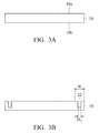
- FIG. 3A to FIG. 3G illustrate an exemplary embodiment of a wafer edge pretreatment for handling a thin wafer. Explanation of the same or similar portions to the description in FIG. 1A to FIG. 1G and FIG. 2A to FIG. 2C is omitted herein.
- FIG. 3A is a cross-sectional view of one embodiment of a wafer 10 provided with a plurality of semiconductor chips therein.
- the wafer 10 has a first surface 10 a and a second surface 10 b opposite top the first surface 10 a , and integrated circuits are formed on the first surface 10 a to connect bond pads and/or other interconnection structures.
- a trench 22 is formed at the edge of the wafer 10 as shown in FIG. 3B , followed by filling a dielectric material, resulting in a support structure 24 as shown in FIG. 3C .
- a carrier 12 is then bonded to the adhesive material layer applied on the first surface 10 a for enabling easier handling of the wafer 10 in subsequent thinning process.
- the trench 22 passes through at least a portion of the edge area of the first surface 10 a down to a predetermined depth of the semiconductor substrate.
- the edge area of the wafer 10 has a width W equal to or less than 10 mm defined from the rim of the wafer 10 .
- the width W is about 2-3 mm.
- the trench 22 has a diameter D 1 of more than 0.1 mm.
- the trench 22 has a diameter D 1 of about 1-2 mm formed within the edge area.
- the trench 22 extends to the semiconductor substrate and is, for example, more than 50 mm in depth.
- the trench 22 is a ring-shaped opening adjacent to the rim of the wafer 10 .
- the dielectric material of the support structure 24 is formed of, for example, a polymer-based material, resin-based material, polyimide, epoxy, SOG, or a combination thereof.
- a wafer thinning process is performed on the second surface 10 b of the wafer 10 to reach a desired thickness as shown in FIG. 3D , wherein the support structure 24 ′′ is also thinned down to be exposed.
- a plurality of dies 14 are bonded onto the thinned wafer 10 ′′ and a protection layer 16 is formed on the dies-to-wafer stack in a molding process as depicted in FIG. 3E .
- the uncovered region 17 exposes at least a part of the support structure 24 ′′.
- the protection layer 16 does not cover the support structure 24 ′′.
- the protection layer 16 covers a part of the support structure 24 ′′.
- the above-described wafer edge pretreatment can be applied for handling a wafer 10 including through vias 40 as depicted in FIGS. 2A to 2C .
- FIGS. 4A to 4G illustrate another exemplary embodiment of a wafer edge pretreatment for handling a thin wafer. Explanation of the same or similar portions to the description in FIGS. 3A to 3G is omitted herein.
- a trench 22 ′′ formed at the edge portion of the wafer 10 as shown in FIG. 4B has a diameter D 2 substantially equal to the width W of the edge area of the first surface 10 a .
- the trench 22 ′′ has a diameter D 2 of about 2-3 mm.
- a support structure 24 a is formed at the edge of the wafer 10 .
- the support structure 24 a is also thinned down and exposed, forming a ring at the rim of the exposed surface 10 b ′′ of the thinned wafer 10 ′′ as shown in FIG. 4D .
- the protection layer 16 is coated over the dies-to-wafer stack and fills the remaining spacing between adjacent dies 14 , but leaves an uncovered region 17 at the edge area of the thinned wafer 10 ′′ for supporting in the molding process.
- the uncovered region 17 exposes at least a part of the support structure 24 a ′′.
- the protection layer 16 does not cover the support structure 24 a ′′.
- the protection layer 16 covers a part of the support structure 24 a′′.
- FIGS. 5A to 5E illustrate an exemplary embodiment of an edge protection method for handling a thin wafer. Explanation of the same or similar portions to the description in FIGS. 1A to 1G is omitted herein.
- a housing 30 is provided for supporting the subsequent molding process as shown in FIG. 5D .
- the housing 30 includes a bottom portion 32 from which a peripheral wall portion 34 extends upwardly to define the concave portion 32 a .
- the dies-to-wafer stack is affixed to the housing 30 by attaching the bottom 12 b of the carrier 12 to the bottom portion 32 using gluing or taping.
- the concave portion 32 a has a planar bottom of an area substantially equal to the bottom area of the carrier 12 , thus the rim of the thinned wafer 10 ′′ is affixed to the peripheral wall portion 34 .
- the housing 30 may be a rigid or a flexible member made from copper, aluminum, plastic, rubber, paper, cardboard, etc.
- a molding process is performed on the dies-to-wafer stack supported by the housing 30 as depicted in FIG. 5E , in which a protection layer 16 can cover the edge of the thinned wafer 10 ′′ without leaving an uncovered region because the peripheral wall portion 34 serves as a support structure for handling the thinned wafer in the molding process and the carrier-detaching process as well.
Abstract
Description
Claims (20)
Priority Applications (3)
| Application Number | Priority Date | Filing Date | Title |
|---|---|---|---|
| US12/717,573 US9117828B2 (en) | 2009-03-27 | 2010-03-04 | Method of handling a thin wafer |
| TW099109332A TWI494979B (en) | 2009-03-27 | 2010-03-29 | Semicondcutor process |
| CN2010101431849A CN101847588B (en) | 2009-03-27 | 2010-03-29 | Semiconductor process |
Applications Claiming Priority (2)
| Application Number | Priority Date | Filing Date | Title |
|---|---|---|---|
| US16411209P | 2009-03-27 | 2009-03-27 | |
| US12/717,573 US9117828B2 (en) | 2009-03-27 | 2010-03-04 | Method of handling a thin wafer |
Publications (2)
| Publication Number | Publication Date |
|---|---|
| US20100248427A1 US20100248427A1 (en) | 2010-09-30 |
| US9117828B2 true US9117828B2 (en) | 2015-08-25 |
Family
ID=42784771
Family Applications (1)
| Application Number | Title | Priority Date | Filing Date |
|---|---|---|---|
| US12/717,573 Expired - Fee Related US9117828B2 (en) | 2009-03-27 | 2010-03-04 | Method of handling a thin wafer |
Country Status (2)
| Country | Link |
|---|---|
| US (1) | US9117828B2 (en) |
| TW (1) | TWI494979B (en) |
Families Citing this family (12)
| Publication number | Priority date | Publication date | Assignee | Title |
|---|---|---|---|---|
| JP2013030537A (en) * | 2011-07-27 | 2013-02-07 | Elpida Memory Inc | Method of manufacturing semiconductor device |
| FR2980917B1 (en) | 2011-09-30 | 2013-09-27 | St Microelectronics Crolles 2 | METHOD FOR PRODUCING AN ELECTRICALLY CONDUCTIVE THROUGH BOND |
| US9111946B2 (en) * | 2012-12-20 | 2015-08-18 | Invensas Corporation | Method of thinning a wafer to provide a raised peripheral edge |
| US8928120B1 (en) * | 2013-06-28 | 2015-01-06 | Taiwan Semiconductor Manufacturing Company Limited | Wafer edge protection structure |
| US9209046B2 (en) * | 2013-10-02 | 2015-12-08 | Taiwan Semiconductor Manufacturing Company Ltd. | Semiconductor device and manufacturing method thereof |
| KR102259959B1 (en) | 2013-12-05 | 2021-06-04 | 삼성전자주식회사 | Carrier and a method of fabricating a semiconductor device |
| US20150371956A1 (en) * | 2014-06-19 | 2015-12-24 | Globalfoundries Inc. | Crackstops for bulk semiconductor wafers |
| JP6369405B2 (en) * | 2015-07-07 | 2018-08-08 | 信越化学工業株式会社 | Thermosetting resin composition for semiconductor encapsulation |
| US10957672B2 (en) * | 2017-11-13 | 2021-03-23 | Taiwan Semiconductor Manufacturing Company, Ltd. | Package structure and method of manufacturing the same |
| CN111180324B (en) * | 2019-12-27 | 2023-04-28 | 中芯集成电路(宁波)有限公司 | Thinning method of bonding wafer structure and wafer level packaging structure |
| CN111667770B (en) * | 2020-07-15 | 2021-10-08 | 武汉华星光电技术有限公司 | Flexible display device |
| US11908831B2 (en) * | 2020-10-21 | 2024-02-20 | Stmicroelectronics Pte Ltd | Method for manufacturing a wafer level chip scale package (WLCSP) |
Citations (51)
| Publication number | Priority date | Publication date | Assignee | Title |
|---|---|---|---|---|
| US4811082A (en) | 1986-11-12 | 1989-03-07 | International Business Machines Corporation | High performance integrated circuit packaging structure |
| US4990462A (en) | 1989-04-12 | 1991-02-05 | Advanced Micro Devices, Inc. | Method for coplanar integration of semiconductor ic devices |
| US5075253A (en) | 1989-04-12 | 1991-12-24 | Advanced Micro Devices, Inc. | Method of coplanar integration of semiconductor IC devices |
| US5380681A (en) | 1994-03-21 | 1995-01-10 | United Microelectronics Corporation | Three-dimensional multichip package and methods of fabricating |
| US6002177A (en) | 1995-12-27 | 1999-12-14 | International Business Machines Corporation | High density integrated circuit packaging with chip stacking and via interconnections |
| US6153536A (en) * | 1999-03-04 | 2000-11-28 | International Business Machines Corporation | Method for mounting wafer frame at back side grinding (BSG) tool |
| US6229216B1 (en) | 1999-01-11 | 2001-05-08 | Intel Corporation | Silicon interposer and multi-chip-module (MCM) with through substrate vias |
| US6271059B1 (en) | 1999-01-04 | 2001-08-07 | International Business Machines Corporation | Chip interconnection structure using stub terminals |
| US6279815B1 (en) | 1998-06-17 | 2001-08-28 | International Business Machines Corporation | Stacked chip process carrier |
| US6333206B1 (en) * | 1996-12-24 | 2001-12-25 | Nitto Denko Corporation | Process for the production of semiconductor device |
| US6355501B1 (en) | 2000-09-21 | 2002-03-12 | International Business Machines Corporation | Three-dimensional chip stacking assembly |
| US6434016B2 (en) | 1999-06-18 | 2002-08-13 | Intel Corporation | Apparatus for interconnecting multiple devices on a circuit board |
| US6448661B1 (en) | 2001-02-09 | 2002-09-10 | Samsung Electornics Co., Ltd. | Three-dimensional multi-chip package having chip selection pads and manufacturing method thereof |
| US6461895B1 (en) | 1999-01-05 | 2002-10-08 | Intel Corporation | Process for making active interposer for high performance packaging applications |
| US6570248B1 (en) | 1998-08-31 | 2003-05-27 | Micron Technology, Inc. | Structure and method for a high-performance electronic packaging assembly |
| US6600222B1 (en) | 2002-07-17 | 2003-07-29 | Intel Corporation | Stacked microelectronic packages |
| US6607938B2 (en) | 2001-07-19 | 2003-08-19 | Samsung Electronics Co., Ltd. | Wafer level stack chip package and method for manufacturing same |
| US6661085B2 (en) | 2002-02-06 | 2003-12-09 | Intel Corporation | Barrier structure against corrosion and contamination in three-dimensional (3-D) wafer-to-wafer vertical stack |
| US6762076B2 (en) | 2002-02-20 | 2004-07-13 | Intel Corporation | Process of vertically stacking multiple wafers supporting different active integrated circuit (IC) devices |
| US6790748B2 (en) | 2002-12-19 | 2004-09-14 | Intel Corporation | Thinning techniques for wafer-to-wafer vertical stacks |
| US20050064681A1 (en) * | 2003-09-19 | 2005-03-24 | Wood Alan G. | Support structure for thinning semiconductor substrates and thinning methods employing the support structure |
| US6887769B2 (en) | 2002-02-06 | 2005-05-03 | Intel Corporation | Dielectric recess for wafer-to-wafer and die-to-die metal bonding and method of fabricating the same |
| US6908785B2 (en) | 2001-12-06 | 2005-06-21 | Samsung Electronics Co., Ltd. | Multi-chip package (MCP) with a conductive bar and method for manufacturing the same |
| US6908565B2 (en) | 2002-12-24 | 2005-06-21 | Intel Corporation | Etch thinning techniques for wafer-to-wafer vertical stacks |
| US6924551B2 (en) | 2003-05-28 | 2005-08-02 | Intel Corporation | Through silicon via, folded flex microelectronic package |
| US6943067B2 (en) | 2002-01-08 | 2005-09-13 | Advanced Micro Devices, Inc. | Three-dimensional integrated semiconductor devices |
| US6946384B2 (en) | 2003-06-06 | 2005-09-20 | Intel Corporation | Stacked device underfill and a method of fabrication |
| US6975016B2 (en) | 2002-02-06 | 2005-12-13 | Intel Corporation | Wafer bonding using a flexible bladder press and thinned wafers for three-dimensional (3D) wafer-to-wafer vertical stack integration, and application thereof |
| US7087538B2 (en) | 2004-08-16 | 2006-08-08 | Intel Corporation | Method to fill the gap between coupled wafers |
| US20060219351A1 (en) * | 2005-04-02 | 2006-10-05 | Stats Chippac Ltd. | Wafer strength reinforcement system for ultra thin wafer thinning |
| US7151009B2 (en) | 2004-06-18 | 2006-12-19 | Samsung Electronics Co., Ltd. | Method for manufacturing wafer level chip stack package |
| US7157353B2 (en) * | 2002-03-06 | 2007-01-02 | Micron Technology, Inc. | Method for fabricating encapsulated semiconductor components |
| US7215033B2 (en) | 2003-11-19 | 2007-05-08 | Samsung Electronics Co., Ltd. | Wafer level stack structure for system-in-package and method thereof |
| US7276799B2 (en) | 2003-08-26 | 2007-10-02 | Samsung Electronics Co., Ltd. | Chip stack package and manufacturing method thereof |
| US7279795B2 (en) | 2005-12-29 | 2007-10-09 | Intel Corporation | Stacked die semiconductor package |
| US7307005B2 (en) | 2004-06-30 | 2007-12-11 | Intel Corporation | Wafer bonding with highly compliant plate having filler material enclosed hollow core |
| US7317256B2 (en) | 2005-06-01 | 2008-01-08 | Intel Corporation | Electronic packaging including die with through silicon via |
| US7320928B2 (en) | 2003-06-20 | 2008-01-22 | Intel Corporation | Method of forming a stacked device filler |
| US7345350B2 (en) | 2003-09-23 | 2008-03-18 | Micron Technology, Inc. | Process and integration scheme for fabricating conductive components, through-vias and semiconductor components including conductive through-wafer vias |
| US7402515B2 (en) | 2005-06-28 | 2008-07-22 | Intel Corporation | Method of forming through-silicon vias with stress buffer collars and resulting devices |
| US7402442B2 (en) | 2005-12-21 | 2008-07-22 | International Business Machines Corporation | Physically highly secure multi-chip assembly |
| US7410884B2 (en) | 2005-11-21 | 2008-08-12 | Intel Corporation | 3D integrated circuits using thick metal for backside connections and offset bumps |
| US7432592B2 (en) | 2005-10-13 | 2008-10-07 | Intel Corporation | Integrated micro-channels for 3D through silicon architectures |
| US20080268614A1 (en) * | 2007-04-25 | 2008-10-30 | Ku-Feng Yang | Wafer Bonding |
| US20090001598A1 (en) * | 2007-06-27 | 2009-01-01 | Wen-Chih Chiou | Formation of Through Via before Contact Processing |
| US7494845B2 (en) | 2004-06-22 | 2009-02-24 | Samsung Electronics Co., Ltd. | Method of forming a thin wafer stack for a wafer level package |
| US7528494B2 (en) | 2005-11-03 | 2009-05-05 | International Business Machines Corporation | Accessible chip stack and process of manufacturing thereof |
| US7557597B2 (en) | 2005-06-03 | 2009-07-07 | International Business Machines Corporation | Stacked chip security |
| US7576435B2 (en) | 2007-04-27 | 2009-08-18 | Taiwan Semiconductor Manufacturing Company, Ltd. | Low-cost and ultra-fine integrated circuit packaging technique |
| US7834450B2 (en) | 2007-08-20 | 2010-11-16 | Samsung Electronics Co., Ltd. | Semiconductor package having memory devices stacked on logic device |
| US7973407B2 (en) * | 2003-07-02 | 2011-07-05 | Intel Corporation | Three-dimensional stacked substrate arrangements |
-
2010
- 2010-03-04 US US12/717,573 patent/US9117828B2/en not_active Expired - Fee Related
- 2010-03-29 TW TW099109332A patent/TWI494979B/en active
Patent Citations (59)
| Publication number | Priority date | Publication date | Assignee | Title |
|---|---|---|---|---|
| US4811082A (en) | 1986-11-12 | 1989-03-07 | International Business Machines Corporation | High performance integrated circuit packaging structure |
| US4990462A (en) | 1989-04-12 | 1991-02-05 | Advanced Micro Devices, Inc. | Method for coplanar integration of semiconductor ic devices |
| US5075253A (en) | 1989-04-12 | 1991-12-24 | Advanced Micro Devices, Inc. | Method of coplanar integration of semiconductor IC devices |
| US5380681A (en) | 1994-03-21 | 1995-01-10 | United Microelectronics Corporation | Three-dimensional multichip package and methods of fabricating |
| US5481133A (en) | 1994-03-21 | 1996-01-02 | United Microelectronics Corporation | Three-dimensional multichip package |
| US6002177A (en) | 1995-12-27 | 1999-12-14 | International Business Machines Corporation | High density integrated circuit packaging with chip stacking and via interconnections |
| US6187678B1 (en) | 1995-12-27 | 2001-02-13 | International Business Machines Corporation | High density integrated circuit packaging with chip stacking and via interconnections |
| US6236115B1 (en) | 1995-12-27 | 2001-05-22 | International Business Machines Corporation | High density integrated circuit packaging with chip stacking and via interconnections |
| US6333206B1 (en) * | 1996-12-24 | 2001-12-25 | Nitto Denko Corporation | Process for the production of semiconductor device |
| US6279815B1 (en) | 1998-06-17 | 2001-08-28 | International Business Machines Corporation | Stacked chip process carrier |
| US6570248B1 (en) | 1998-08-31 | 2003-05-27 | Micron Technology, Inc. | Structure and method for a high-performance electronic packaging assembly |
| US6271059B1 (en) | 1999-01-04 | 2001-08-07 | International Business Machines Corporation | Chip interconnection structure using stub terminals |
| US6461895B1 (en) | 1999-01-05 | 2002-10-08 | Intel Corporation | Process for making active interposer for high performance packaging applications |
| US6229216B1 (en) | 1999-01-11 | 2001-05-08 | Intel Corporation | Silicon interposer and multi-chip-module (MCM) with through substrate vias |
| US6562653B1 (en) | 1999-01-11 | 2003-05-13 | Intel Corporation | Silicon interposer and multi-chip-module (MCM) with through substrate vias |
| US6153536A (en) * | 1999-03-04 | 2000-11-28 | International Business Machines Corporation | Method for mounting wafer frame at back side grinding (BSG) tool |
| US6434016B2 (en) | 1999-06-18 | 2002-08-13 | Intel Corporation | Apparatus for interconnecting multiple devices on a circuit board |
| US6355501B1 (en) | 2000-09-21 | 2002-03-12 | International Business Machines Corporation | Three-dimensional chip stacking assembly |
| US6448661B1 (en) | 2001-02-09 | 2002-09-10 | Samsung Electornics Co., Ltd. | Three-dimensional multi-chip package having chip selection pads and manufacturing method thereof |
| US6607938B2 (en) | 2001-07-19 | 2003-08-19 | Samsung Electronics Co., Ltd. | Wafer level stack chip package and method for manufacturing same |
| US7531890B2 (en) | 2001-12-06 | 2009-05-12 | Samsung Electronics Co., Ltd. | Multi-chip package (MCP) with a conductive bar and method for manufacturing the same |
| US6908785B2 (en) | 2001-12-06 | 2005-06-21 | Samsung Electronics Co., Ltd. | Multi-chip package (MCP) with a conductive bar and method for manufacturing the same |
| US6943067B2 (en) | 2002-01-08 | 2005-09-13 | Advanced Micro Devices, Inc. | Three-dimensional integrated semiconductor devices |
| US7056807B2 (en) | 2002-02-06 | 2006-06-06 | Intel Corporation | Barrier structure against corrosion and contamination in three-dimensional (3-D) wafer-to-wafer vertical stack |
| US6887769B2 (en) | 2002-02-06 | 2005-05-03 | Intel Corporation | Dielectric recess for wafer-to-wafer and die-to-die metal bonding and method of fabricating the same |
| US6661085B2 (en) | 2002-02-06 | 2003-12-09 | Intel Corporation | Barrier structure against corrosion and contamination in three-dimensional (3-D) wafer-to-wafer vertical stack |
| US6975016B2 (en) | 2002-02-06 | 2005-12-13 | Intel Corporation | Wafer bonding using a flexible bladder press and thinned wafers for three-dimensional (3D) wafer-to-wafer vertical stack integration, and application thereof |
| US7037804B2 (en) | 2002-02-06 | 2006-05-02 | Intel Corporation | Wafer bonding using a flexible bladder press for three dimensional (3D) vertical stack integration |
| US6762076B2 (en) | 2002-02-20 | 2004-07-13 | Intel Corporation | Process of vertically stacking multiple wafers supporting different active integrated circuit (IC) devices |
| US7157787B2 (en) | 2002-02-20 | 2007-01-02 | Intel Corporation | Process of vertically stacking multiple wafers supporting different active integrated circuit (IC) devices |
| US7157353B2 (en) * | 2002-03-06 | 2007-01-02 | Micron Technology, Inc. | Method for fabricating encapsulated semiconductor components |
| US6600222B1 (en) | 2002-07-17 | 2003-07-29 | Intel Corporation | Stacked microelectronic packages |
| US6790748B2 (en) | 2002-12-19 | 2004-09-14 | Intel Corporation | Thinning techniques for wafer-to-wafer vertical stacks |
| US6908565B2 (en) | 2002-12-24 | 2005-06-21 | Intel Corporation | Etch thinning techniques for wafer-to-wafer vertical stacks |
| US6924551B2 (en) | 2003-05-28 | 2005-08-02 | Intel Corporation | Through silicon via, folded flex microelectronic package |
| US6946384B2 (en) | 2003-06-06 | 2005-09-20 | Intel Corporation | Stacked device underfill and a method of fabrication |
| US7320928B2 (en) | 2003-06-20 | 2008-01-22 | Intel Corporation | Method of forming a stacked device filler |
| US7973407B2 (en) * | 2003-07-02 | 2011-07-05 | Intel Corporation | Three-dimensional stacked substrate arrangements |
| US7276799B2 (en) | 2003-08-26 | 2007-10-02 | Samsung Electronics Co., Ltd. | Chip stack package and manufacturing method thereof |
| US20050064681A1 (en) * | 2003-09-19 | 2005-03-24 | Wood Alan G. | Support structure for thinning semiconductor substrates and thinning methods employing the support structure |
| US7345350B2 (en) | 2003-09-23 | 2008-03-18 | Micron Technology, Inc. | Process and integration scheme for fabricating conductive components, through-vias and semiconductor components including conductive through-wafer vias |
| US7215033B2 (en) | 2003-11-19 | 2007-05-08 | Samsung Electronics Co., Ltd. | Wafer level stack structure for system-in-package and method thereof |
| US7151009B2 (en) | 2004-06-18 | 2006-12-19 | Samsung Electronics Co., Ltd. | Method for manufacturing wafer level chip stack package |
| US7494845B2 (en) | 2004-06-22 | 2009-02-24 | Samsung Electronics Co., Ltd. | Method of forming a thin wafer stack for a wafer level package |
| US7307005B2 (en) | 2004-06-30 | 2007-12-11 | Intel Corporation | Wafer bonding with highly compliant plate having filler material enclosed hollow core |
| US7087538B2 (en) | 2004-08-16 | 2006-08-08 | Intel Corporation | Method to fill the gap between coupled wafers |
| US20060219351A1 (en) * | 2005-04-02 | 2006-10-05 | Stats Chippac Ltd. | Wafer strength reinforcement system for ultra thin wafer thinning |
| US7317256B2 (en) | 2005-06-01 | 2008-01-08 | Intel Corporation | Electronic packaging including die with through silicon via |
| US7557597B2 (en) | 2005-06-03 | 2009-07-07 | International Business Machines Corporation | Stacked chip security |
| US7402515B2 (en) | 2005-06-28 | 2008-07-22 | Intel Corporation | Method of forming through-silicon vias with stress buffer collars and resulting devices |
| US7432592B2 (en) | 2005-10-13 | 2008-10-07 | Intel Corporation | Integrated micro-channels for 3D through silicon architectures |
| US7528494B2 (en) | 2005-11-03 | 2009-05-05 | International Business Machines Corporation | Accessible chip stack and process of manufacturing thereof |
| US7410884B2 (en) | 2005-11-21 | 2008-08-12 | Intel Corporation | 3D integrated circuits using thick metal for backside connections and offset bumps |
| US7402442B2 (en) | 2005-12-21 | 2008-07-22 | International Business Machines Corporation | Physically highly secure multi-chip assembly |
| US7279795B2 (en) | 2005-12-29 | 2007-10-09 | Intel Corporation | Stacked die semiconductor package |
| US20080268614A1 (en) * | 2007-04-25 | 2008-10-30 | Ku-Feng Yang | Wafer Bonding |
| US7576435B2 (en) | 2007-04-27 | 2009-08-18 | Taiwan Semiconductor Manufacturing Company, Ltd. | Low-cost and ultra-fine integrated circuit packaging technique |
| US20090001598A1 (en) * | 2007-06-27 | 2009-01-01 | Wen-Chih Chiou | Formation of Through Via before Contact Processing |
| US7834450B2 (en) | 2007-08-20 | 2010-11-16 | Samsung Electronics Co., Ltd. | Semiconductor package having memory devices stacked on logic device |
Also Published As
| Publication number | Publication date |
|---|---|
| TW201036055A (en) | 2010-10-01 |
| TWI494979B (en) | 2015-08-01 |
| US20100248427A1 (en) | 2010-09-30 |
Similar Documents
| Publication | Publication Date | Title |
|---|---|---|
| US9117828B2 (en) | Method of handling a thin wafer | |
| US8441136B2 (en) | Protection layer for adhesive material at wafer edge | |
| US11631611B2 (en) | Wafer level chip scale packaging intermediate structure apparatus and method | |
| US10790235B2 (en) | Integrated fan-out package and method of fabricating the same | |
| US10636773B2 (en) | Semiconductor package structure and method for forming the same | |
| US7883991B1 (en) | Temporary carrier bonding and detaching processes | |
| CN107026092B (en) | Method of manufacturing fingerprint scanner and semiconductor device | |
| TWI556349B (en) | Semiconductor device structure and fabricating method thereof | |
| US10424563B2 (en) | Semiconductor package assembly and method for forming the same | |
| KR101157726B1 (en) | Ultra-thin stacked chips packaging | |
| US11676906B2 (en) | Chip package and manufacturing method thereof | |
| US11776838B2 (en) | Semiconductor package and manufacturing method thereof | |
| US11342321B2 (en) | Manufacturing method of package on package structure | |
| US20230207472A1 (en) | Semiconductor package and manufacturing method of semiconductor package | |
| US20190067226A1 (en) | Integrated circuit component package and method of fabricating the same | |
| TWI767287B (en) | A semiconductor package structure | |
| US11244879B2 (en) | Semiconductor package | |
| US11848233B2 (en) | Semiconductor package and manufacturing method thereof | |
| CN101847588B (en) | Semiconductor process | |
| US10991597B2 (en) | Method of fabricating a semiconductor device using an adhesive layer |
Legal Events
| Date | Code | Title | Description |
|---|---|---|---|
| AS | Assignment |
Owner name: TAIWAN SEMICONDUCTOR MANUFACTURING COMPANY, LTD., Free format text: ASSIGNMENT OF ASSIGNORS INTEREST;ASSIGNORS:WU, WENG-JIN;YANG, KU-FENG;CHIOU, WEN-CHIH;REEL/FRAME:024030/0094 Effective date: 20100225 |
|
| ZAAA | Notice of allowance and fees due |
Free format text: ORIGINAL CODE: NOA |
|
| ZAAB | Notice of allowance mailed |
Free format text: ORIGINAL CODE: MN/=. |
|
| STCF | Information on status: patent grant |
Free format text: PATENTED CASE |
|
| MAFP | Maintenance fee payment |
Free format text: PAYMENT OF MAINTENANCE FEE, 4TH YEAR, LARGE ENTITY (ORIGINAL EVENT CODE: M1551); ENTITY STATUS OF PATENT OWNER: LARGE ENTITY Year of fee payment: 4 |
|
| FEPP | Fee payment procedure |
Free format text: MAINTENANCE FEE REMINDER MAILED (ORIGINAL EVENT CODE: REM.); ENTITY STATUS OF PATENT OWNER: LARGE ENTITY |
|
| LAPS | Lapse for failure to pay maintenance fees |
Free format text: PATENT EXPIRED FOR FAILURE TO PAY MAINTENANCE FEES (ORIGINAL EVENT CODE: EXP.); ENTITY STATUS OF PATENT OWNER: LARGE ENTITY |
|
| STCH | Information on status: patent discontinuation |
Free format text: PATENT EXPIRED DUE TO NONPAYMENT OF MAINTENANCE FEES UNDER 37 CFR 1.362 |
|
| FP | Lapsed due to failure to pay maintenance fee |
Effective date: 20230825 |