US9799585B2 - Method for forming a case for an electronic device and manufactured case structure for electronic device - Google Patents

Method for forming a case for an electronic device and manufactured case structure for electronic device Download PDF

Info

Publication number
US9799585B2
US9799585B2 US14/249,084 US201414249084A US9799585B2 US 9799585 B2 US9799585 B2 US 9799585B2 US 201414249084 A US201414249084 A US 201414249084A US 9799585 B2 US9799585 B2 US 9799585B2
Authority
US
United States
Prior art keywords
electronic device
case
pcm microcapsules
capsule shell
pcm
Prior art date
Legal status (The legal status is an assumption and is not a legal conclusion. Google has not performed a legal analysis and makes no representation as to the accuracy of the status listed.)
Active, expires
Application number
US14/249,084
Other versions
US20140367607A1 (en
Inventor
Chih-Ming WENG
Yi-Lun Cheng
Chun-Lung Lin
Current Assignee (The listed assignees may be inaccurate. Google has not performed a legal analysis and makes no representation or warranty as to the accuracy of the list.)
Inventec Pudong Technology Corp
Inventec Corp
Original Assignee
Inventec Pudong Technology Corp
Inventec Corp
Priority date (The priority date is an assumption and is not a legal conclusion. Google has not performed a legal analysis and makes no representation as to the accuracy of the date listed.)
Filing date
Publication date
Application filed by Inventec Pudong Technology Corp, Inventec Corp filed Critical Inventec Pudong Technology Corp
Assigned to INVENTEC (PUDONG) TECHNOLOGY CORPORATION, INVENTEC CORPORATION reassignment INVENTEC (PUDONG) TECHNOLOGY CORPORATION ASSIGNMENT OF ASSIGNORS INTEREST (SEE DOCUMENT FOR DETAILS). Assignors: CHENG, YI-LUN, LIN, CHUN-LUNG, WENG, CHIH-MING
Publication of US20140367607A1 publication Critical patent/US20140367607A1/en
Application granted granted Critical
Publication of US9799585B2 publication Critical patent/US9799585B2/en
Active legal-status Critical Current
Adjusted expiration legal-status Critical

Links

Images

Classifications

    • HELECTRICITY
    • H01ELECTRIC ELEMENTS
    • H01LSEMICONDUCTOR DEVICES NOT COVERED BY CLASS H10
    • H01L23/00Details of semiconductor or other solid state devices
    • H01L23/34Arrangements for cooling, heating, ventilating or temperature compensation ; Temperature sensing arrangements
    • H01L23/42Fillings or auxiliary members in containers or encapsulations selected or arranged to facilitate heating or cooling
    • H01L23/427Cooling by change of state, e.g. use of heat pipes
    • H01L23/4275Cooling by change of state, e.g. use of heat pipes by melting or evaporation of solids
    • BPERFORMING OPERATIONS; TRANSPORTING
    • B29WORKING OF PLASTICS; WORKING OF SUBSTANCES IN A PLASTIC STATE IN GENERAL
    • B29CSHAPING OR JOINING OF PLASTICS; SHAPING OF MATERIAL IN A PLASTIC STATE, NOT OTHERWISE PROVIDED FOR; AFTER-TREATMENT OF THE SHAPED PRODUCTS, e.g. REPAIRING
    • B29C45/00Injection moulding, i.e. forcing the required volume of moulding material through a nozzle into a closed mould; Apparatus therefor
    • B29C45/0001Injection moulding, i.e. forcing the required volume of moulding material through a nozzle into a closed mould; Apparatus therefor characterised by the choice of material
    • FMECHANICAL ENGINEERING; LIGHTING; HEATING; WEAPONS; BLASTING
    • F28HEAT EXCHANGE IN GENERAL
    • F28DHEAT-EXCHANGE APPARATUS, NOT PROVIDED FOR IN ANOTHER SUBCLASS, IN WHICH THE HEAT-EXCHANGE MEDIA DO NOT COME INTO DIRECT CONTACT
    • F28D20/00Heat storage plants or apparatus in general; Regenerative heat-exchange apparatus not covered by groups F28D17/00 or F28D19/00
    • F28D20/02Heat storage plants or apparatus in general; Regenerative heat-exchange apparatus not covered by groups F28D17/00 or F28D19/00 using latent heat
    • F28D20/023Heat storage plants or apparatus in general; Regenerative heat-exchange apparatus not covered by groups F28D17/00 or F28D19/00 using latent heat the latent heat storage material being enclosed in granular particles or dispersed in a porous, fibrous or cellular structure
    • HELECTRICITY
    • H02GENERATION; CONVERSION OR DISTRIBUTION OF ELECTRIC POWER
    • H02KDYNAMO-ELECTRIC MACHINES
    • H02K5/00Casings; Enclosures; Supports
    • H02K5/02Casings or enclosures characterised by the material thereof
    • HELECTRICITY
    • H05ELECTRIC TECHNIQUES NOT OTHERWISE PROVIDED FOR
    • H05KPRINTED CIRCUITS; CASINGS OR CONSTRUCTIONAL DETAILS OF ELECTRIC APPARATUS; MANUFACTURE OF ASSEMBLAGES OF ELECTRICAL COMPONENTS
    • H05K7/00Constructional details common to different types of electric apparatus
    • H05K7/20Modifications to facilitate cooling, ventilating, or heating
    • H05K7/2039Modifications to facilitate cooling, ventilating, or heating characterised by the heat transfer by conduction from the heat generating element to a dissipating body
    • BPERFORMING OPERATIONS; TRANSPORTING
    • B29WORKING OF PLASTICS; WORKING OF SUBSTANCES IN A PLASTIC STATE IN GENERAL
    • B29LINDEXING SCHEME ASSOCIATED WITH SUBCLASS B29C, RELATING TO PARTICULAR ARTICLES
    • B29L2031/00Other particular articles
    • B29L2031/34Electrical apparatus, e.g. sparking plugs or parts thereof
    • B29L2031/3481Housings or casings incorporating or embedding electric or electronic elements
    • HELECTRICITY
    • H01ELECTRIC ELEMENTS
    • H01LSEMICONDUCTOR DEVICES NOT COVERED BY CLASS H10
    • H01L2924/00Indexing scheme for arrangements or methods for connecting or disconnecting semiconductor or solid-state bodies as covered by H01L24/00
    • HELECTRICITY
    • H01ELECTRIC ELEMENTS
    • H01LSEMICONDUCTOR DEVICES NOT COVERED BY CLASS H10
    • H01L2924/00Indexing scheme for arrangements or methods for connecting or disconnecting semiconductor or solid-state bodies as covered by H01L24/00
    • H01L2924/0001Technical content checked by a classifier
    • H01L2924/0002Not covered by any one of groups H01L24/00, H01L24/00 and H01L2224/00
    • YGENERAL TAGGING OF NEW TECHNOLOGICAL DEVELOPMENTS; GENERAL TAGGING OF CROSS-SECTIONAL TECHNOLOGIES SPANNING OVER SEVERAL SECTIONS OF THE IPC; TECHNICAL SUBJECTS COVERED BY FORMER USPC CROSS-REFERENCE ART COLLECTIONS [XRACs] AND DIGESTS
    • Y02TECHNOLOGIES OR APPLICATIONS FOR MITIGATION OR ADAPTATION AGAINST CLIMATE CHANGE
    • Y02EREDUCTION OF GREENHOUSE GAS [GHG] EMISSIONS, RELATED TO ENERGY GENERATION, TRANSMISSION OR DISTRIBUTION
    • Y02E60/00Enabling technologies; Technologies with a potential or indirect contribution to GHG emissions mitigation
    • Y02E60/14Thermal energy storage
    • Y02E60/145

Definitions

  • the disclosure relates to a method for forming a case for an electronic device and a manufactured case structure for an electronic device, and more particularly, to a method for forming a case and a manufactured case structure for an electronic device by using phase change material (PCM) microcapsules.
  • PCM phase change material
  • a method for forming a case for an electronic device comprises the following steps. Provide a plastic material. Provide a plurality of phase change material (PCM) microcapsules. Mix the plastic material and the plurality of PCM microcapsules so as to form a housing material. Form a case for an electronic device from the housing material by injection molding.
  • PCM phase change material
  • a case structure for an electronic device comprises a plastic layer and a plurality of PCM microcapsules.
  • the PCM microcapsules are dispersed in the plastic layer.
  • FIG. 1 is a flow chart of a method for forming a case for an electronic device according to an embodiment of the disclosure
  • FIG. 2 is a sectional view of a PCM microcapsule in Step 102 of FIG. 1 ;
  • FIG. 3 is a schematic diagram of a housing material in Step 103 of FIG. 1 ;
  • FIG. 4 is a sectional view of part of the structure of a case structure for an electronic device formed according to the method of FIG. 1 .
  • FIG. 1 is a flow chart of a method for forming a case for an electronic device according to an embodiment of the disclosure
  • FIG. 2 is a sectional view of a phase change material (PCM) microcapsule in Step 102 of FIG. 1
  • FIG. 3 is a schematic diagram of a housing material in Step 103 of FIG. 1 .
  • PCM phase change material
  • the plastic material is polycarbonate/acrylonitrile-butadiene-styrene (PC/ABS), but the disclosure is not limited thereto.
  • PC/ABS polycarbonate/acrylonitrile-butadiene-styrene
  • each of the PCM microcapsules 30 comprises a capsule shell 32 and a capsule core 34 .
  • the capsule core 34 is enclosed by the capsule shell 32 .
  • the material of the capsule shell 32 is a polymer
  • the material of the capsule core 34 comprises a phase change material.
  • the melting point of the phase change material is between 20° C. and 75° C., preferably, between 35° C. and 55° C.
  • the material of the capsule shell 32 comprises a mixture of polycarbonate (PC) and glass fiber (GF).
  • the mass percentage of glass fiber (GF) in the capsule shell 32 is between 35% and 45%, preferably, 40%.
  • the material of the capsule core 34 comprises a phase change material.
  • the phase change material is a heat absorbing substance, for example, paraffin wax, alkanes (e.g. icosane to triacontane), alcohols (e.g. decan-1-ol to icosane-1-ol), and acids (e.g. decanoic acid to icosanoic acid).
  • the material and the composition of the capsule shell 32 and the capsule core 34 are not limited to the disclosure.
  • the diameter of the PCM microcapsules is between 0.1 and 1000 micrometers ( ⁇ m), preferably, between 10 and 30 micrometers, and more preferably, between 20 and 30 micrometers.
  • the material of the capsule shell 32 corresponds to the plastic material. More specifically, the melting point of the capsule shell 32 is higher than the melting point of the plastic material.
  • the melting point of the capsule shell 32 (PC/GF) is about 285° C.
  • the melting point of the plastic material (PC/ABS) is about 230° C.
  • Step 103 mix the plastic material and the phase change material so as to form a housing material (Step 103 ) (as shown in FIG. 3 ).
  • the volume ratio of the plastic material to the PCM microcapsules is between 4:1 and 99:1, preferably, 4:1 to 9:1.
  • the plastic material 20 and the PCM microcapsules 30 are mixed with the volume ratio of 4:1, but the disclosure is not limited thereto.
  • a user can adjust the volume ratio of the plastic material 20 and the PCM microcapsule 30 according to his/her need.
  • the PCM microcapsules 30 are dispersed uniformly in the plastic material 20 .
  • Step 104 form a case for an electronic device from the housing material by injection molding.
  • the housing material passes through a machine for injection molding (not shown), and the housing material is molded to form a case for an electronic device under a reaction temperature.
  • the reaction temperature is lower than the melting point of the capsule shell of the PCM microcapsules, as well as the reaction temperature is higher than the melting point of the plastic material. Therefore, the plastic material is liquefied during the reaction because of the high temperature, so that the user can mold the plastic material to the designed shape according to his/her need.
  • the capsule shell keeps in a solid phase and restricts the capsule core enclosed by the capsule shell during the reaction.
  • FIG. 4 is a sectional view of part of the structure of a case structure for an electronic device formed according to the method of FIG. 1 .
  • the formed case structure 10 for an electronic device comprises a plastic layer 20 ′ and a plurality of PCM microcapsules 30 .
  • the PCM microcapsules 30 are dispersed uniformly in the plastic layer 20 ′.
  • each of the PCM microcapsules 30 has a capsule shell 32 and a capsule core 34 , and the capsule core 34 is enclosed by the capsule shell 32 .
  • the material and composition of the capsule shell 32 and the capsule core 34 are described above.
  • the material of the capsule core 34 in the PCM microcapsules 30 is a phase change material, as well, the phase change material has high latent heat, therefore, when electronic units produce a great amount of heat and the heat is delivered to the case structure 10 for an electronic device, the phase change material absorbs and stores the heat so as to proceed a phase transition. Temperature is kept in a range during the phase transition, as well; the temperature is controlled by adjusting the capsule core 34 of the PCM microcapsules 30 . Therefore, the phase change material slows down the rising of the temperature, as well as improving the heat dissipation of the case structure 10 for an electronic device. Further, heat dissipation of the surface of the case structure 10 for an electronic device is controlled and the temperature of the surface of the case structure 10 for an electronic device is maintained in thermostatic.
  • the plastic material is mixed with the PCM microcapsules and forms the case structure for electronic device by injection molding. Therefore, the manufactured case structure for an electronic device does not need further machining, and the process is simplified. Furthermore, the case structure for electronic device absorbs heat by the PCM microcapsules, so that the heat dissipation of the case structure for an electronic device is better. Therefore, the problems met in prior art that the manufacturing of the cases is complicated and the heat dissipation of the manufactured case structures is not desirable have been solved.

Abstract

A method for forming a case for an electronic device and a manufactured case structure for an electronic device are provided. The method for forming a case for an electronic device comprises the following steps. Provide a plastic material. Provide a plurality of PCM microcapsules. Mix the plastic material and the plurality of PCM microcapsules so as to form a housing material. Form a case from the housing material by injection molding. The manufactured case structure for an electronic device comprises a plastic layer and a plurality of PCM microcapsules. The plurality of PCM microcapsules are dispersed in the plastic layer.

Description

CROSS-REFERENCE TO RELATED APPLICATIONS
This non-provisional application claims priority under 35 U.S.C. §119(a) on Patent Application No(s). 201310239169.8 filed in China on Jun. 17, 2013, the entire contents of which are hereby incorporated by reference.
BACKGROUND OF THE INVENTION
Technical Field of the Invention
The disclosure relates to a method for forming a case for an electronic device and a manufactured case structure for an electronic device, and more particularly, to a method for forming a case and a manufactured case structure for an electronic device by using phase change material (PCM) microcapsules.
Description of the Related Art
With the improvement of technologies, the market for electronic devices (e.g. notebooks, portable mobile phones, tablet computers, electronic dictionaries, or portable electronic gaming machines) has become more and more competitive. In order to meet the consumers' needs, the industry has invested a lot of money for researching. With the improvement of the performance of electronic devices, electronic devices are producing more and more heat while working. In order to improve heat dissipation of electronic devices, aluminum foils or graphene sheets are usually attached to the plastic case, so as to dissipate the heat. However, the process needs to be done after the manufacturing of the plastic cases, and the process increases the producing cost of the cases. On the other hand, different cases usually have different sizes, so that one size of the aluminum foils or the graphene sheets can not be attached uniformly on cases with different sizes, as well the heat dissipation is affected. Therefore, how to design a method for forming a case and the case structure thereof, so as to solve the problems met in prior art that the manufacturing of the cases is complicated and the heat dissipation of the manufactured case structures is not desirable, has become the problems designers need to solve.
SUMMARY OF THE INVENTION
According to an embodiment, a method for forming a case for an electronic device is disclosed. The method comprises the following steps. Provide a plastic material. Provide a plurality of phase change material (PCM) microcapsules. Mix the plastic material and the plurality of PCM microcapsules so as to form a housing material. Form a case for an electronic device from the housing material by injection molding.
According to an embodiment, a case structure for an electronic device is disclosed. The case structure for an electronic device comprises a plastic layer and a plurality of PCM microcapsules. The PCM microcapsules are dispersed in the plastic layer.
BRIEF DESCRIPTION OF THE DRAWINGS
The present disclosure will become more fully understood from the detailed description given herein below for illustration only, thus does not limit the present disclosure, wherein:
FIG. 1 is a flow chart of a method for forming a case for an electronic device according to an embodiment of the disclosure;
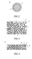
FIG. 2 is a sectional view of a PCM microcapsule in Step 102 of FIG. 1;
FIG. 3 is a schematic diagram of a housing material in Step 103 of FIG. 1;
FIG. 4 is a sectional view of part of the structure of a case structure for an electronic device formed according to the method of FIG. 1.
DETAILED DESCRIPTION
In the following detailed description, for purposes of explanation, numerous specific details are set forth in order to provide a thorough understanding of the disclosed embodiments. It will be apparent, however, that one or more embodiments may be practiced without these specific details. In other instances, well-known structures and devices are schematically shown in order to simplify the drawing.
Please refer to FIGS. 1-3, FIG. 1 is a flow chart of a method for forming a case for an electronic device according to an embodiment of the disclosure, FIG. 2 is a sectional view of a phase change material (PCM) microcapsule in Step 102 of FIG. 1, and FIG. 3 is a schematic diagram of a housing material in Step 103 of FIG. 1.
First, provide a plastic material (Step 101). In this embodiment, the plastic material is polycarbonate/acrylonitrile-butadiene-styrene (PC/ABS), but the disclosure is not limited thereto.
Then, provide a plurality of PCM microcapsules (Step 102) (as shown in FIG. 2). In this embodiment, each of the PCM microcapsules 30 comprises a capsule shell 32 and a capsule core 34. The capsule core 34 is enclosed by the capsule shell 32. Wherein, the material of the capsule shell 32 is a polymer, and the material of the capsule core 34 comprises a phase change material. The melting point of the phase change material is between 20° C. and 75° C., preferably, between 35° C. and 55° C. In this embodiment, the material of the capsule shell 32 comprises a mixture of polycarbonate (PC) and glass fiber (GF). In this and some other embodiments, the mass percentage of glass fiber (GF) in the capsule shell 32 is between 35% and 45%, preferably, 40%. Furthermore, the material of the capsule core 34 comprises a phase change material. The phase change material is a heat absorbing substance, for example, paraffin wax, alkanes (e.g. icosane to triacontane), alcohols (e.g. decan-1-ol to icosane-1-ol), and acids (e.g. decanoic acid to icosanoic acid). However, the material and the composition of the capsule shell 32 and the capsule core 34 are not limited to the disclosure. In this embodiment, the diameter of the PCM microcapsules is between 0.1 and 1000 micrometers (μm), preferably, between 10 and 30 micrometers, and more preferably, between 20 and 30 micrometers.
In this and other embodiments, the material of the capsule shell 32 corresponds to the plastic material. More specifically, the melting point of the capsule shell 32 is higher than the melting point of the plastic material. For example, in this embodiment, the melting point of the capsule shell 32 (PC/GF) is about 285° C., and the melting point of the plastic material (PC/ABS) is about 230° C.
Afterwards, mix the plastic material and the phase change material so as to form a housing material (Step 103) (as shown in FIG. 3). The volume ratio of the plastic material to the PCM microcapsules is between 4:1 and 99:1, preferably, 4:1 to 9:1. In this embodiment, the plastic material 20 and the PCM microcapsules 30 are mixed with the volume ratio of 4:1, but the disclosure is not limited thereto. A user can adjust the volume ratio of the plastic material 20 and the PCM microcapsule 30 according to his/her need. After the mixing process of Step 103, the PCM microcapsules 30 are dispersed uniformly in the plastic material 20.
Finally, form a case for an electronic device from the housing material by injection molding (Step 104). In detail, the housing material passes through a machine for injection molding (not shown), and the housing material is molded to form a case for an electronic device under a reaction temperature. In this and other embodiments, when the housing material passes through the machine for injection molding, the reaction temperature is lower than the melting point of the capsule shell of the PCM microcapsules, as well as the reaction temperature is higher than the melting point of the plastic material. Therefore, the plastic material is liquefied during the reaction because of the high temperature, so that the user can mold the plastic material to the designed shape according to his/her need. Furthermore, the capsule shell keeps in a solid phase and restricts the capsule core enclosed by the capsule shell during the reaction.
Please refer to FIG. 4, FIG. 4 is a sectional view of part of the structure of a case structure for an electronic device formed according to the method of FIG. 1. The formed case structure 10 for an electronic device comprises a plastic layer 20′ and a plurality of PCM microcapsules 30. The PCM microcapsules 30 are dispersed uniformly in the plastic layer 20′. In detail, each of the PCM microcapsules 30 has a capsule shell 32 and a capsule core 34, and the capsule core 34 is enclosed by the capsule shell 32. Wherein, the material and composition of the capsule shell 32 and the capsule core 34 are described above.
Since the case structure for an electronic device 10 comprises a plurality of PCM microcapsules 30, the material of the capsule core 34 in the PCM microcapsules 30 is a phase change material, as well, the phase change material has high latent heat, therefore, when electronic units produce a great amount of heat and the heat is delivered to the case structure 10 for an electronic device, the phase change material absorbs and stores the heat so as to proceed a phase transition. Temperature is kept in a range during the phase transition, as well; the temperature is controlled by adjusting the capsule core 34 of the PCM microcapsules 30. Therefore, the phase change material slows down the rising of the temperature, as well as improving the heat dissipation of the case structure 10 for an electronic device. Further, heat dissipation of the surface of the case structure 10 for an electronic device is controlled and the temperature of the surface of the case structure 10 for an electronic device is maintained in thermostatic.
According to the method for forming a case for an electronic device and the manufactured case structure for an electronic device of the disclosure, the plastic material is mixed with the PCM microcapsules and forms the case structure for electronic device by injection molding. Therefore, the manufactured case structure for an electronic device does not need further machining, and the process is simplified. Furthermore, the case structure for electronic device absorbs heat by the PCM microcapsules, so that the heat dissipation of the case structure for an electronic device is better. Therefore, the problems met in prior art that the manufacturing of the cases is complicated and the heat dissipation of the manufactured case structures is not desirable have been solved.
The embodiments were chosen and described in order to explain the principles of the disclosure and their practical application so as to activate others skilled in the art to utilize the disclosure and various embodiments and with various modifications as are suited to the particular use contemplated. Alternative embodiments will become apparent to those skilled in the art to which the present disclosure pertains without departing from its spirit and scope. Accordingly, the scope of the present disclosure is defined by the appended claims rather than the foregoing description and the exemplary embodiments described therein.

Claims (6)

What is claimed is:
1. A method for forming a case for an electronic device, comprising:
providing a plastic material;
providing a plurality of phase change material (PCM) microcapsules;
mixing the plastic material and the plurality of PCM microcapsules so as to form a housing material; and
forming a case for an electronic device from the housing material by injection molding,
wherein each of the plurality of PCM microcapsules comprises a capsule shell and a capsule core, the capsule core is enclosed by the capsule shell, the material of the capsule shell is a polymer, the material of the capsule core comprises a phase change material, and a melting point of the phase change material is between 20° C. and 75° C., and
wherein the melting point of the capsule shell of the plurality of PCM microcapsules is higher than the melting point of the plastic material.
2. The method for forming a case for an electronic device according to claim 1, wherein the housing material forms the case for an electronic device by injection molding under a reaction temperature, the reaction temperature is lower than the melting point of the capsule shell of the plurality of PCM microcapsules, the reaction temperature is higher than the melting point of the plastic material.
3. The method for forming a case for an electronic device according to claim 1, wherein in the steps of mixing the plastic material and the plurality of PCM microcapsules so as to form the housing material, the volume ratio of the plastic material to the plurality of PCM microcapsules is between 4:1 and 99:1.
4. A case structure for an electronic device, comprising:
a plastic layer; and
a plurality of PCM microcapsules, dispersing in the plastic layer,
wherein each of the plurality of PCM microcapsules comprises a capsule shell and a capsule core, the capsule core is enclosed by the capsule shell, the material of the capsule shell is a polymer, the material of the capsule core comprises a phase change material, and a melting point of the phase change material is between 20° C. and 75° C., and
wherein the melting point of the capsule shell of the plurality of PCM microcapsules is higher than the melting point of the plastic layer.
5. The case structure for an electronic device according to claim 4, wherein the material of the capsule shell of the plurality of PCM microcapsules comprises a polycarbonate and a glass fiber.
6. The case structure for an electronic device according to claim 4, wherein the volume ratio of the plastic layer to the plurality of PCM microcapsules is between 4:1 and 99:1.
US14/249,084 2013-06-17 2014-04-09 Method for forming a case for an electronic device and manufactured case structure for electronic device Active 2036-08-21 US9799585B2 (en)

Applications Claiming Priority (3)

Application Number Priority Date Filing Date Title
CN201310239169 2013-06-17
CN201310239169.8A CN104227913A (en) 2013-06-17 2013-06-17 Forming method of electronic device shell and electronic device shell structure manufactured thereby
CN201310239169.8 2013-06-17

Publications (2)

Publication Number Publication Date
US20140367607A1 US20140367607A1 (en) 2014-12-18
US9799585B2 true US9799585B2 (en) 2017-10-24

Family

ID=52018431

Family Applications (1)

Application Number Title Priority Date Filing Date
US14/249,084 Active 2036-08-21 US9799585B2 (en) 2013-06-17 2014-04-09 Method for forming a case for an electronic device and manufactured case structure for electronic device

Country Status (2)

Country Link
US (1) US9799585B2 (en)
CN (1) CN104227913A (en)

Cited By (1)

* Cited by examiner, † Cited by third party
Publication number Priority date Publication date Assignee Title
US11670570B2 (en) 2019-05-22 2023-06-06 Samsung Electronics Co., Ltd. Electronic device and method of manufacturing an electronic device

Families Citing this family (7)

* Cited by examiner, † Cited by third party
Publication number Priority date Publication date Assignee Title
CN105744810B (en) * 2016-04-29 2018-12-11 广东欧珀移动通信有限公司 A kind of shell and mobile terminal of terminal
CN108601292B (en) * 2016-04-29 2020-07-21 Oppo广东移动通信有限公司 Rear shell and mobile terminal
CN107567243A (en) * 2017-08-17 2018-01-09 深圳天珑无线科技有限公司 Housing and preparation method thereof, electronic installation
KR102329343B1 (en) * 2018-09-11 2021-11-18 주식회사 엘지에너지솔루션 Battery module with enhanced cooling efficiency and Battery pack comprising the same
US11067343B2 (en) * 2018-10-25 2021-07-20 Toyota Motor Engineering & Manufacturing North America, Inc. Thermal compensation layers with core-shell phase change particles and power electronics assemblies incorporating the same
US10575393B1 (en) * 2018-11-13 2020-02-25 International Business Machines Corporation Heat-shielding microcapsules for protecting temperature sensitive components
CN112497595A (en) * 2020-11-12 2021-03-16 西安紫光国芯半导体有限公司 Preparation method and application of flexible heat dissipation shell

Citations (2)

* Cited by examiner, † Cited by third party
Publication number Priority date Publication date Assignee Title
US8587945B1 (en) * 2012-07-27 2013-11-19 Outlast Technologies Llc Systems structures and materials for electronic device cooling
US9282679B2 (en) * 2013-11-29 2016-03-08 Inventec (Pudong) Technology Corporation Electronic device with phase change material microcapsule layer

Family Cites Families (5)

* Cited by examiner, † Cited by third party
Publication number Priority date Publication date Assignee Title
CN2824518Y (en) * 2005-06-03 2006-10-04 华为技术有限公司 Mobile terminal apparatus with heat storage material
US20090154113A1 (en) * 2007-12-12 2009-06-18 Inter Corporation Thermal energy storage for mobile computing thermal management
CN101709119A (en) * 2009-07-27 2010-05-19 张世忠 Phase-change energy storage plastic
KR101283793B1 (en) * 2009-09-21 2013-07-08 (주)엘지하우시스 Functional inorganic board and manufacturing method thereof
CN102548355B (en) * 2010-12-31 2015-04-29 联想(北京)有限公司 Electronic equipment

Patent Citations (2)

* Cited by examiner, † Cited by third party
Publication number Priority date Publication date Assignee Title
US8587945B1 (en) * 2012-07-27 2013-11-19 Outlast Technologies Llc Systems structures and materials for electronic device cooling
US9282679B2 (en) * 2013-11-29 2016-03-08 Inventec (Pudong) Technology Corporation Electronic device with phase change material microcapsule layer

Cited By (1)

* Cited by examiner, † Cited by third party
Publication number Priority date Publication date Assignee Title
US11670570B2 (en) 2019-05-22 2023-06-06 Samsung Electronics Co., Ltd. Electronic device and method of manufacturing an electronic device

Also Published As

Publication number Publication date
US20140367607A1 (en) 2014-12-18
CN104227913A (en) 2014-12-24

Similar Documents

Publication Publication Date Title
US9799585B2 (en) Method for forming a case for an electronic device and manufactured case structure for electronic device
Ding et al. 4D rods: 3D structures via programmable 1D composite rods
Lewicki et al. 3D-printing of meso-structurally ordered carbon fiber/polymer composites with unprecedented orthotropic physical properties
US9226428B2 (en) High heat capacity electronic components and methods for fabricating
WO2016165250A1 (en) Flexible substrate and manufacturing method thereof, display substrate and display device
CN105744811A (en) Housing and mobile terminal
TW201700589A (en) Acylic resin heat dissipation foam sheet
CN104072966A (en) Multi-element composite heat-conducting functional master batch and preparation method thereof
TWI510158B (en) Method for manufacturing case of electronic devices and manufactured case structure of electronic devices
TW201717728A (en) Strengthenned blind cover and production method thereof
CN106061198A (en) Screen assembly and mobile terminal
US9426914B2 (en) Film insert molding for device manufacture
JPWO2014155898A1 (en) Insulation sheet and manufacturing method thereof
CN105828551A (en) Rear shell and mobile terminal
US20140370216A1 (en) Case structure for an electronic device and manufacturing method thereof
CN108148554A (en) Cooling fin filled compositions, cooling fin and preparation method thereof
KR100838112B1 (en) Mobile Phone Using Phase Change Materials, Manufacturing Method Thereof
CN103965535A (en) Preparation method of heat-conductive plastic adopting ordered space network structure
CN114085652A (en) Heat-conducting composite material and preparation method thereof
CN105825783A (en) Display screen bracket and terminal
Calvo Structural relaxation in Ag-Ni nanoparticles: atomistic modeling away from equilibrium
CN106003944B (en) There is one kind high-strength PC to be modified carrier material
CN104076422B (en) Reflectance coating and preparation method thereof
CN102554241A (en) Method for preparing foam conglomerated copper powder
JP2020070309A (en) Composite material and method for producing the same

Legal Events

Date Code Title Description
AS Assignment

Owner name: INVENTEC (PUDONG) TECHNOLOGY CORPORATION, CHINA

Free format text: ASSIGNMENT OF ASSIGNORS INTEREST;ASSIGNORS:WENG, CHIH-MING;CHENG, YI-LUN;LIN, CHUN-LUNG;REEL/FRAME:032638/0546

Effective date: 20140326

Owner name: INVENTEC CORPORATION, TAIWAN

Free format text: ASSIGNMENT OF ASSIGNORS INTEREST;ASSIGNORS:WENG, CHIH-MING;CHENG, YI-LUN;LIN, CHUN-LUNG;REEL/FRAME:032638/0546

Effective date: 20140326

STCF Information on status: patent grant

Free format text: PATENTED CASE

MAFP Maintenance fee payment

Free format text: PAYMENT OF MAINTENANCE FEE, 4TH YEAR, LARGE ENTITY (ORIGINAL EVENT CODE: M1551); ENTITY STATUS OF PATENT OWNER: LARGE ENTITY

Year of fee payment: 4